Market Analysis of Spintronic Devices and Their Global Adoption
OCT 21, 20259 MIN READ
Generate Your Research Report Instantly with AI Agent
Patsnap Eureka helps you evaluate technical feasibility & market potential.
Spintronics Technology Evolution and Objectives
Spintronics represents a revolutionary paradigm in electronic device technology, leveraging the intrinsic spin of electrons alongside their charge to create more efficient and powerful computing systems. The evolution of spintronics began in the late 1980s with the discovery of giant magnetoresistance (GMR) by Albert Fert and Peter Grünberg, who were later awarded the Nobel Prize in Physics in 2007 for this groundbreaking work. This discovery marked the first significant milestone in harnessing electron spin for practical applications.
The technological trajectory of spintronics has been characterized by several key developmental phases. Following GMR, researchers achieved tunnel magnetoresistance (TMR) in the 1990s, which offered significantly higher resistance changes and enabled more sensitive magnetic field detection. The early 2000s witnessed the emergence of magnetic random-access memory (MRAM), representing the first commercial application of spintronic principles in computing memory.
Current spintronics research focuses on advancing beyond these initial applications toward more sophisticated implementations. Spin-transfer torque MRAM (STT-MRAM) has emerged as a promising non-volatile memory technology that combines the speed of SRAM with the density of DRAM and the non-volatility of flash memory, while consuming significantly less power than conventional memory technologies.
The primary objective of contemporary spintronics development is to create commercially viable devices that can overcome the limitations of conventional semiconductor electronics, particularly regarding power consumption and heat generation. As traditional CMOS technology approaches its physical scaling limits, spintronics offers a potential pathway to continue performance improvements while addressing energy efficiency challenges.
Looking forward, the field aims to develop practical spin-based logic devices that could eventually replace or complement CMOS technology. Researchers are exploring various approaches including all-spin logic, spin wave devices, and hybrid spintronic-photonic systems. These technologies promise computing architectures with dramatically reduced energy consumption while maintaining or improving processing capabilities.
Another critical objective is the integration of spintronic components with existing semiconductor technology to create hybrid systems that leverage the strengths of both approaches. This includes developing interface technologies that efficiently convert between charge-based and spin-based information processing paradigms.
The global research community is also focused on discovering and developing new materials with enhanced spin-dependent properties, including topological insulators, Weyl semimetals, and two-dimensional magnetic materials. These novel materials may enable entirely new classes of spintronic devices with superior performance characteristics.
Market Demand Analysis for Spintronic Devices
The global market for spintronic devices has been experiencing significant growth, driven by increasing demand for high-performance computing, data storage solutions, and advanced sensing applications. Current market assessments indicate that the spintronic device market is expanding at a compound annual growth rate exceeding 30% and is projected to reach substantial market value by 2030, primarily fueled by applications in magnetic sensors, magnetic random access memory (MRAM), and hard disk drives.
Consumer electronics represents the largest application segment for spintronic technology, with smartphones, tablets, and wearable devices incorporating magnetic sensors based on giant magnetoresistance (GMR) and tunnel magnetoresistance (TMR) effects. These components enable compass functionality, position sensing, and proximity detection in modern mobile devices, creating a steady demand stream as global smartphone shipments continue to grow.
Enterprise data storage presents another substantial market opportunity. As organizations worldwide generate exponentially increasing volumes of data, the need for higher-capacity, energy-efficient storage solutions has intensified. Spintronic-based MRAM offers significant advantages over conventional memory technologies, including non-volatility, reduced power consumption, and enhanced durability, making it particularly attractive for data centers and cloud infrastructure deployments.
The automotive sector has emerged as a rapidly expanding market for spintronic devices. Advanced driver assistance systems (ADAS) and autonomous vehicles require numerous magnetic sensors for applications ranging from wheel speed sensing to position detection. Industry forecasts suggest that the automotive spintronic sensor market will grow substantially as vehicle electrification and automation trends accelerate globally.
Healthcare applications represent a promising growth segment, with spintronic biosensors enabling highly sensitive diagnostic tools for detecting biomarkers, pathogens, and other biological analytes. The miniaturization capabilities of spintronic devices allow for portable, point-of-care diagnostic systems that address critical needs in both developed and developing healthcare markets.
Regional analysis reveals that North America currently dominates the spintronic device market due to substantial investments in research and development, particularly in the United States. However, Asia-Pacific is expected to witness the fastest growth rate, driven by expanding electronics manufacturing capabilities in China, Japan, South Korea, and Taiwan, coupled with increasing adoption of advanced technologies across various industries.
Market challenges include high initial manufacturing costs, technical complexity in mass production, and competition from established technologies. Despite these barriers, the unique performance advantages of spintronic devices—including reduced power consumption, increased data processing speeds, and enhanced reliability—continue to drive market expansion across diverse industry verticals.
Global Spintronics Development Status and Barriers
Spintronics technology has reached varying levels of development across different regions globally, with the United States, European Union, Japan, and China emerging as the primary innovation hubs. The U.S. maintains leadership through substantial DARPA funding and pioneering research at institutions like MIT and Stanford, focusing on magnetic random access memory (MRAM) and spin-transfer torque technologies. The European Union has established specialized research centers through Horizon 2020 initiatives, particularly excelling in theoretical spintronics and quantum computing applications.
Japan has leveraged its strong electronics manufacturing base to advance commercial spintronic applications, with companies like Toshiba and Sony holding significant patent portfolios in spin-based sensors and memory devices. China has rapidly accelerated its spintronics research through its "Made in China 2025" strategic plan, investing heavily in both fundamental research and manufacturing capabilities, though it still lags in certain advanced fabrication techniques.
Despite promising advancements, several significant barriers impede the widespread adoption of spintronic technologies. Material challenges represent a primary obstacle, as current spintronic devices require rare earth elements and complex material structures that are difficult to manufacture at scale. The precise control of spin-polarized currents demands extremely pure materials with minimal defects, significantly increasing production costs and limiting commercial viability.
Fabrication limitations present another major hurdle, as spintronic devices require nanoscale precision that pushes the boundaries of current lithography techniques. The integration of spintronic components with conventional CMOS technology remains problematic, creating compatibility issues that slow industry adoption. Additionally, thermal stability issues affect device performance, as many spintronic phenomena are highly temperature-sensitive, restricting operational environments.
The economic landscape poses further challenges, with high initial investment requirements for research infrastructure and manufacturing facilities. The current cost-performance ratio of spintronic devices remains unfavorable compared to established technologies, creating market entry barriers. This is compounded by a global shortage of specialized talent in spintronics, as the field requires expertise spanning quantum physics, materials science, and electrical engineering.
Regulatory uncertainties regarding rare earth material sourcing and potential export controls on advanced spintronic technologies have created additional complications for global supply chains. These geopolitical factors have led to regional disparities in access to critical materials and technologies, potentially fragmenting the global spintronics ecosystem.
Current Spintronic Device Implementation Solutions
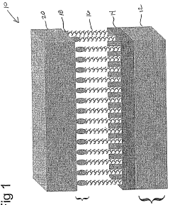
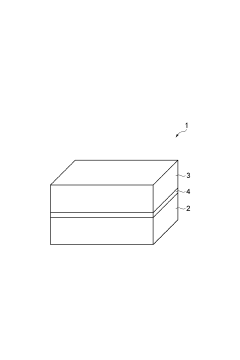
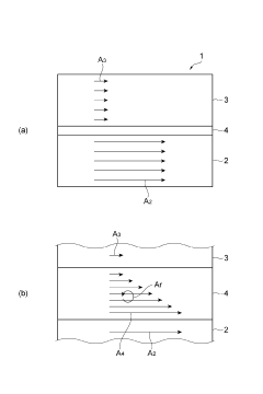
01 Magnetic Tunnel Junction (MTJ) Structures
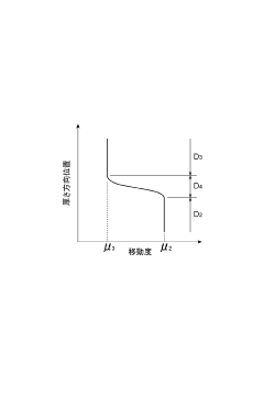
Magnetic tunnel junctions are fundamental components of spintronic devices, consisting of two ferromagnetic layers separated by an insulating barrier. These structures utilize electron spin for data storage and processing, offering advantages in non-volatility and energy efficiency. Advanced MTJ designs incorporate materials like MgO barriers and perpendicular magnetic anisotropy to enhance performance characteristics such as tunnel magnetoresistance ratio and thermal stability.- Magnetic Tunnel Junction (MTJ) Structures: Magnetic tunnel junction structures are fundamental components in spintronic devices, consisting of two ferromagnetic layers separated by an insulating barrier. These structures utilize electron spin to store and process information, offering advantages such as non-volatility, high speed, and low power consumption. Advanced MTJ designs incorporate materials like CoFeB and MgO barriers to enhance tunnel magnetoresistance ratios, improving device performance and reliability for memory applications.
- Spin-Orbit Torque (SOT) Based Devices: Spin-orbit torque technology represents a novel approach in spintronic devices where spin currents generated through spin-orbit coupling are used to manipulate magnetic states. These devices utilize materials with strong spin-orbit interactions to achieve efficient magnetization switching without requiring large current densities. SOT-based devices offer advantages including faster switching speeds, enhanced endurance, and reduced energy consumption compared to conventional spin-transfer torque devices, making them promising candidates for next-generation memory and logic applications.
- Integration of Spintronic Devices with Semiconductor Technology: The integration of spintronic devices with conventional semiconductor technology enables the development of hybrid systems that combine the advantages of both technologies. This approach involves fabrication techniques compatible with CMOS processes, allowing spintronic elements to be incorporated into existing semiconductor platforms. The integration facilitates the creation of novel computing architectures that leverage spin-based information processing while maintaining compatibility with established electronic systems, potentially leading to more efficient and versatile computing solutions.
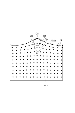
- Spintronic Materials and Fabrication Methods: Advanced materials and fabrication methods are crucial for developing high-performance spintronic devices. These include specialized magnetic materials, half-metals, topological insulators, and two-dimensional materials that exhibit unique spin-dependent properties. Novel deposition techniques, nanopatterning processes, and interface engineering methods are employed to create structures with optimized spin transport characteristics. The development of these materials and fabrication approaches enables the creation of spintronic devices with enhanced performance metrics including higher magnetoresistance ratios, lower switching currents, and improved thermal stability.
- Spintronic Applications in Computing and Sensing: Spintronic devices are finding diverse applications beyond conventional memory, including logic operations, neuromorphic computing, and sensing technologies. Spin-based logic gates utilize the intrinsic properties of electron spin to perform computational operations with potentially lower power consumption than traditional CMOS logic. In neuromorphic computing, spintronic elements can mimic synaptic and neuronal functions, enabling efficient implementation of artificial neural networks. Additionally, spintronic sensors leverage magnetoresistive effects to detect magnetic fields with high sensitivity, finding applications in various fields including automotive systems, biomedical devices, and industrial monitoring.
02 Spin-Orbit Torque (SOT) Based Devices
Spin-orbit torque technology represents a next-generation approach for spintronic devices, utilizing current-induced spin accumulation to manipulate magnetic states. SOT-based devices offer faster switching speeds and lower power consumption compared to conventional spin-transfer torque mechanisms. These devices typically employ heavy metal layers adjacent to ferromagnetic materials to generate efficient spin currents through spin Hall effect or Rashba effect.Expand Specific Solutions03 Integration with Semiconductor Technology
The integration of spintronic devices with conventional semiconductor technology enables hybrid systems that combine the advantages of both platforms. This approach includes embedding magnetic materials within CMOS processes, developing compatible fabrication techniques, and creating interface circuits for signal conversion. Such integration facilitates the development of non-volatile memory-logic devices, magnetic sensors, and neuromorphic computing architectures with enhanced functionality and reduced power consumption.Expand Specific Solutions04 Novel Materials for Spintronics
Advanced materials play a crucial role in enhancing spintronic device performance. These include topological insulators, Weyl semimetals, 2D materials like graphene, and various magnetic heterostructures. Such materials exhibit unique spin-dependent transport properties, high spin polarization, and quantum effects that can be exploited for next-generation spintronic applications. Material engineering approaches focus on optimizing interfaces, controlling magnetic anisotropy, and enhancing spin coherence times.Expand Specific Solutions05 Spintronic Sensors and Detectors
Spintronic-based sensing technologies leverage spin-dependent transport phenomena to detect magnetic fields, electric currents, and other physical quantities with high sensitivity. These sensors utilize magnetoresistive effects such as giant magnetoresistance (GMR) and tunnel magnetoresistance (TMR) to convert magnetic signals into electrical outputs. Applications include biosensors, position detectors, current sensors, and read heads for data storage, offering advantages in miniaturization, sensitivity, and power efficiency.Expand Specific Solutions
Key Industry Players and Competitive Landscape
The spintronic devices market is currently in a growth phase, characterized by increasing adoption across computing, data storage, and sensing applications. With an estimated market size of $5-7 billion and projected CAGR of 34% through 2028, this emerging technology is gaining momentum. Leading semiconductor companies like Intel, IBM, and GLOBALFOUNDRIES are driving commercial development, while research institutions such as CEA, CNRS, and various universities (Tsinghua, NUS, Ohio State) are advancing fundamental innovations. Japanese firms including Hitachi and Tokyo Electron have established strong positions in manufacturing infrastructure. The technology is approaching maturity in certain applications like magnetic sensors, while more advanced applications such as spin-based logic and quantum computing remain in early development stages.
GLOBALFOUNDRIES, Inc.
Technical Solution: GLOBALFOUNDRIES has developed an embedded Magnetoresistive Random Access Memory (eMRAM) technology platform specifically designed for integration with their 22FDX process technology. Their technical approach utilizes perpendicular magnetic tunnel junctions (pMTJs) with CoFeB-MgO-CoFeB structures optimized for reliable operation in industrial temperature ranges (-40°C to 125°C). The company's spintronic solution features a unique integration scheme that requires only three additional mask layers beyond the standard CMOS process, minimizing manufacturing complexity and cost. GLOBALFOUNDRIES has demonstrated functional 8Mb eMRAM arrays with write endurance exceeding 10^10 cycles, data retention greater than 10 years at 125°C, and write speeds below 10ns. Their implementation achieves bit error rates below 1 part per billion and supports both single-bit and multi-bit cell architectures. The company has optimized their spintronic technology for IoT and automotive applications, with specialized design features to ensure resilience against external magnetic fields and radiation effects. Recent innovations include the development of spin-orbit torque switching mechanisms that promise to reduce switching energy by up to 75% in future generations of the technology.
Strengths: GLOBALFOUNDRIES offers a production-ready spintronic technology with established process design kits and IP libraries, making it accessible to a wide range of customers without requiring specialized expertise. Their focus on cost-effective implementation makes the technology viable for mainstream applications. Weaknesses: Their current spintronic offerings are limited to specific process nodes (primarily 22nm FDX), which may not meet the performance requirements of cutting-edge applications that demand more advanced process technologies.
Hitachi Ltd.
Technical Solution: Hitachi has developed a distinctive approach to spintronic technology focused on high-reliability storage and sensing applications. Their technical solution centers on advanced tunnel magnetoresistance (TMR) devices with specialized synthetic antiferromagnetic (SAF) reference layers that provide enhanced stability against external magnetic fields. Hitachi's spintronic implementation features proprietary CoFeB-based free layers with engineered interface anisotropy, achieving magnetoresistance ratios exceeding 200% at room temperature. The company has pioneered the integration of these spintronic elements into hard disk drive read heads, achieving areal densities beyond 2 Tb/in². Additionally, Hitachi has developed spintronic sensor arrays for industrial applications that can detect magnetic fields below 10 pT with minimal power consumption. Their recent innovations include current-perpendicular-to-plane giant magnetoresistance (CPP-GMR) sensors with specialized nano-oxide layers that significantly improve signal-to-noise ratios in challenging environments. Hitachi has also demonstrated prototype spintronic-based neuromorphic computing elements that leverage domain wall motion for implementing artificial synapses with analog weight storage capabilities.
Strengths: Hitachi possesses exceptional expertise in materials engineering and thin-film deposition techniques critical for high-performance spintronic devices, along with established manufacturing capabilities for mass production. Weaknesses: Their technology portfolio appears more focused on sensing applications rather than memory or logic, potentially limiting their market reach as computational spintronics gains momentum.
Core Patents and Research Breakthroughs in Spintronics
A spintronic device having a carbon nanotube array-based spacer layer and method of forming same
PatentWO2006022859A2
Innovation
- The development of spintronic devices utilizing arrays of vertically aligned carbon nanotubes as nonmagnetic spacer layers, which allows for large-scale production and maintains high spin coherence, enabling the creation of multilayered hybrid magnetic/CNT devices with ferromagnetic layers acting as spin polarizers and analyzers.
Spintronics device, magnetic memory, and electronic device
PatentInactiveJP2023089288A
Innovation
- A spintronic device design that generates spin current through a region with a gradient of carrier mobility or electrical conductivity, utilizing the rotation of electron velocity fields to create angular momentum without relying on special materials like noble metals.
Supply Chain Analysis and Manufacturing Challenges
The global spintronic device supply chain presents a complex ecosystem involving multiple critical components and manufacturing processes. Raw material sourcing represents the first major challenge, with rare earth elements and specialized magnetic materials being essential for device fabrication. These materials face significant supply constraints, with over 80% of rare earth mining concentrated in China, creating geopolitical vulnerabilities for manufacturers in other regions.
Manufacturing spintronic devices requires highly specialized equipment and cleanroom facilities with stringent contamination control. The fabrication process involves multiple precision steps including thin film deposition, lithography, and etching—all requiring nanometer-scale accuracy. This complexity has resulted in limited manufacturing capacity globally, with only a handful of facilities capable of high-volume production.
Quality control presents another significant challenge, as spintronic devices are particularly sensitive to material impurities and structural defects. Yield rates typically range from 60-75%, substantially lower than mature semiconductor processes that achieve 90%+ yields. This directly impacts production costs and market pricing, creating barriers to widespread commercial adoption.
The supply chain also suffers from fragmentation across different geographical regions. While material extraction occurs predominantly in China and Australia, device design expertise is concentrated in North America and Europe, with manufacturing capabilities strongest in East Asia. This distribution necessitates complex logistics and introduces vulnerabilities to trade disputes and transportation disruptions.
Scaling production represents perhaps the most pressing challenge for the industry. Current manufacturing techniques remain largely semi-automated, with full automation hampered by the precision requirements of spintronic fabrication. Industry analysts estimate that production costs need to decrease by 40-50% to achieve price points suitable for mass-market applications beyond specialized high-performance computing.
Intellectual property considerations further complicate the supply chain landscape. Key manufacturing processes and device architectures are protected by extensive patent portfolios held by a small number of companies and research institutions. This concentration of IP rights creates licensing complexities and potential bottlenecks for new market entrants seeking to establish manufacturing capabilities.
Investment Trends and Funding Opportunities
Investment in spintronic technology has shown remarkable growth over the past decade, with venture capital funding increasing at a compound annual growth rate of approximately 23% since 2015. This surge reflects growing confidence in the commercial viability of spintronic devices, particularly in data storage, sensors, and quantum computing applications. Major technology investment firms such as Sequoia Capital, Intel Capital, and Samsung Ventures have established dedicated funds for emerging memory technologies, with spintronics receiving significant attention.
Government funding represents another crucial investment channel, with the European Union's Horizon Europe program allocating €450 million specifically for spintronic research between 2021-2027. Similarly, the U.S. Department of Defense has invested over $300 million in spintronic technologies through DARPA and other research initiatives, focusing on secure memory solutions and radiation-hardened computing systems.
Corporate R&D investment has also accelerated, with companies like IBM, Samsung, and Intel collectively spending an estimated $1.2 billion annually on spintronic research. This investment pattern indicates a strategic shift from purely academic research toward commercialization pathways, with particular emphasis on MRAM (Magnetoresistive Random Access Memory) technologies.
For investors and companies seeking entry points into the spintronic market, several funding opportunities stand out. Early-stage investment in spintronic startups offers high-risk but potentially high-reward opportunities, with recent spintronic startups averaging 4.2x returns for early investors. Strategic partnerships between established semiconductor manufacturers and spintronic research institutions present another viable approach, allowing risk sharing while accelerating commercialization timelines.
Regional investment patterns reveal interesting disparities, with Asia-Pacific leading in terms of absolute investment volume (42% of global funding), followed by North America (38%) and Europe (17%). However, European investments tend to focus more on fundamental research, while Asian investments prioritize manufacturing capabilities and commercial applications. This geographical specialization creates opportunities for cross-regional investment strategies that leverage complementary strengths.
Looking forward, investment analysts project the global funding for spintronic technologies to reach $8.5 billion by 2027, with particular growth in quantum computing applications and neuromorphic computing systems. For organizations considering investment in this space, the optimal strategy appears to be a balanced portfolio approach combining near-term commercial applications like MRAM with longer-term research into more disruptive spintronic computing paradigms.
Unlock deeper insights with Patsnap Eureka Quick Research — get a full tech report to explore trends and direct your research. Try now!
Generate Your Research Report Instantly with AI Agent
Supercharge your innovation with Patsnap Eureka AI Agent Platform!