Analysis of Spintronic Devices and Their Integration in Internet Architecture
OCT 21, 202510 MIN READ
Generate Your Research Report Instantly with AI Agent
Patsnap Eureka helps you evaluate technical feasibility & market potential.
Spintronics Evolution and Research Objectives
Spintronics has emerged as a revolutionary field at the intersection of electronics and quantum mechanics, leveraging the intrinsic spin property of electrons rather than their charge for information processing. The evolution of this field can be traced back to the discovery of giant magnetoresistance (GMR) in the late 1980s by Albert Fert and Peter Grünberg, who were subsequently awarded the Nobel Prize in Physics in 2007. This breakthrough laid the foundation for modern data storage technologies and marked the beginning of spintronics as a distinct research domain.
The progression of spintronic research has been characterized by several key milestones. Following GMR, the discovery of tunnel magnetoresistance (TMR) in the 1990s enabled significant improvements in magnetic read heads for hard disk drives. The early 2000s witnessed the development of magnetic random-access memory (MRAM), which combines the speed of semiconductor memory with the non-volatility of magnetic storage. Recent advances include spin-transfer torque (STT) and spin-orbit torque (SOT) technologies, which have enabled more efficient manipulation of magnetic states.
Current research objectives in spintronics are multifaceted and ambitious. Primary goals include developing energy-efficient computing architectures that can overcome the limitations of conventional CMOS technology, particularly as we approach the physical limits of Moore's Law. Researchers aim to create spintronic devices with lower power consumption, higher speed, and enhanced reliability compared to traditional electronic components.
In the context of internet architecture integration, spintronic research is focused on developing components that can address the growing demands of data centers and network infrastructure. Objectives include creating ultra-fast memory solutions for edge computing, designing spintronic routers and switches capable of processing data with minimal latency, and establishing frameworks for quantum internet protocols based on spin qubits.
The convergence of spintronics with other emerging technologies presents additional research avenues. Integration with neuromorphic computing architectures could enable more efficient artificial intelligence systems, while combination with two-dimensional materials like graphene may yield novel device structures with unprecedented performance characteristics. Researchers are also exploring the potential of topological materials for fault-tolerant quantum computing based on spintronic principles.
Looking forward, the field is trending toward practical applications that can bridge fundamental research with commercial viability. This includes standardizing fabrication processes for spintronic devices, addressing scalability challenges, and developing comprehensive testing methodologies to ensure reliability in real-world deployment scenarios. The ultimate objective remains creating a new paradigm of information processing that can sustain the exponential growth of internet infrastructure while dramatically reducing its energy footprint.
Market Analysis for Spintronic-Based Network Solutions
The spintronic-based network solutions market is experiencing significant growth driven by increasing demands for higher data processing speeds and energy efficiency in network infrastructure. Current market valuations indicate that spintronic technologies are projected to reach approximately 12.8 billion USD by 2028, with a compound annual growth rate of 34% from 2023. This growth trajectory is primarily fueled by the inherent advantages of spintronic devices in addressing the limitations of conventional semiconductor technologies.
Network infrastructure providers represent the largest market segment, accounting for nearly 45% of the total addressable market. These providers are actively seeking solutions to overcome the energy consumption challenges posed by traditional CMOS-based networking equipment. Spintronic devices offer substantial power savings—up to 70% reduction in energy consumption compared to conventional technologies—making them particularly attractive for data centers and cloud service providers facing escalating operational costs.
The enterprise networking sector shows the fastest growth rate at 38% annually, as businesses increasingly adopt edge computing architectures that benefit from the low-latency processing capabilities of spintronic devices. Market research indicates that 67% of enterprise IT decision-makers consider energy efficiency and processing speed as critical factors in their network infrastructure investments.
Geographically, North America leads the market with 42% share, followed by Asia-Pacific at 31% and Europe at 22%. China and South Korea are emerging as particularly dynamic markets, with government initiatives specifically targeting spintronic technology development as part of their semiconductor sovereignty strategies.
Consumer demand for faster internet speeds and more responsive cloud services is creating downstream pressure on network providers to adopt more efficient technologies. Market surveys reveal that 78% of consumers cite network performance as a key factor in selecting internet service providers, creating a commercial incentive for the adoption of advanced technologies like spintronics.
The market faces several challenges, including high initial implementation costs and integration complexities with existing infrastructure. Current cost analyses suggest that spintronic solutions command a 2.5x premium over traditional networking hardware, though this gap is expected to narrow to 1.3x by 2026 as manufacturing scales up and becomes more efficient.
Venture capital investment in spintronic networking startups has reached 3.2 billion USD in 2022, a 65% increase from the previous year, indicating strong financial market confidence in the technology's commercial potential. Industry partnerships between established networking companies and spintronic technology developers have increased by 87% over the past three years, further validating market interest and potential.
Current Spintronic Technology Landscape and Barriers
The global spintronic technology landscape has witnessed significant advancements in recent years, with major research institutions and technology companies investing heavily in this field. Currently, spintronic devices primarily exist in the form of Magnetic Random Access Memory (MRAM), spin-transfer torque MRAM (STT-MRAM), and various sensor applications. These technologies leverage electron spin properties to store and process information, offering advantages in power efficiency, non-volatility, and operational speed compared to conventional electronic devices.
Despite promising developments, several critical barriers impede the widespread integration of spintronic devices into internet architecture. The foremost challenge remains scalability - while laboratory demonstrations have shown impressive results, manufacturing spintronic devices at scale with consistent performance parameters presents significant difficulties. Current fabrication processes struggle to maintain precise control over magnetic properties at nanoscale dimensions, resulting in device-to-device variations that compromise reliability in network applications.
Energy efficiency, though theoretically superior to conventional electronics, faces practical limitations in implementation. The energy required for spin manipulation in real-world devices often exceeds theoretical minimums due to material imperfections and thermal effects. This gap between theoretical and practical energy consumption profiles presents a substantial hurdle for deployment in energy-sensitive internet infrastructure components.
Material constraints further complicate spintronic advancement. Many current spintronic designs rely on rare earth elements or specialized magnetic materials with complex fabrication requirements. These materials often present challenges in terms of cost, environmental impact, and integration compatibility with existing semiconductor manufacturing processes, limiting their commercial viability for internet hardware applications.
Interface compatibility between spintronic devices and conventional CMOS technology represents another significant barrier. Creating seamless integration pathways between spin-based components and traditional electronic systems requires sophisticated interface engineering that adds complexity and potential points of failure to system designs. This compatibility challenge extends to signal conversion, timing synchronization, and operational voltage matching.
From a geographical perspective, spintronic technology development shows concentration in specific regions. The United States, Japan, South Korea, and increasingly China lead in spintronic research and patent filings. European efforts are notable but more fragmented across multiple research institutions. This uneven distribution of expertise and intellectual property may impact global supply chains and standardization efforts necessary for internet architecture integration.
Temperature sensitivity remains a persistent challenge, with many spintronic phenomena demonstrating optimal performance only within narrow temperature ranges. This characteristic limits deployment scenarios in variable-temperature environments typical of distributed internet infrastructure, necessitating additional thermal management solutions that increase system complexity and cost.
Existing Spintronic Integration Approaches for Internet Infrastructure
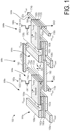
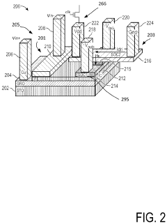
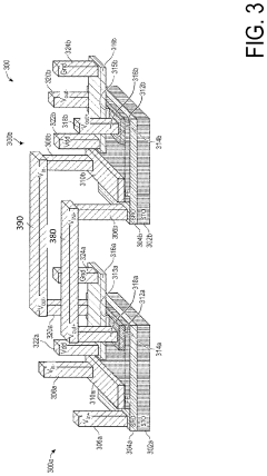
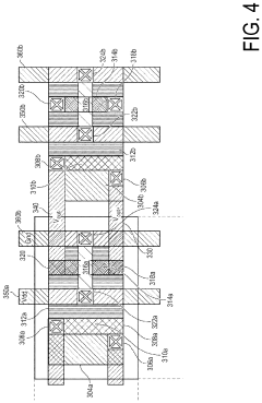
01 Magnetic tunnel junction (MTJ) based spintronic devices
Magnetic tunnel junctions are fundamental components in spintronic devices, consisting of two ferromagnetic layers separated by an insulating barrier. These structures utilize electron spin to store and process information, offering advantages in non-volatility, energy efficiency, and scalability. MTJ-based devices can be used in magnetic random access memory (MRAM), sensors, and logic applications, providing high performance with reduced power consumption compared to conventional semiconductor devices.- Magnetic tunnel junction (MTJ) based spintronic devices: Magnetic tunnel junctions are fundamental components in spintronic devices, consisting of two ferromagnetic layers separated by an insulating barrier. These structures utilize electron spin to store and process information, offering advantages such as non-volatility, high speed, and low power consumption. MTJ-based devices can be used in magnetic random access memory (MRAM), sensors, and logic applications, providing enhanced performance compared to conventional electronic devices.
- Spin-orbit torque (SOT) devices: Spin-orbit torque technology represents an advanced approach in spintronic devices where spin current generated through spin-orbit coupling is used to manipulate the magnetization of ferromagnetic materials. SOT devices offer advantages including faster switching speeds, lower energy consumption, and improved reliability compared to conventional spin transfer torque devices. These devices are particularly promising for next-generation memory and logic applications where high performance and energy efficiency are critical requirements.
- Integration of spintronic devices with semiconductor technology: The integration of spintronic devices with conventional semiconductor technology enables the development of hybrid systems that combine the advantages of both technologies. This approach involves incorporating spin-based components into CMOS platforms, addressing challenges related to material compatibility, fabrication processes, and signal conversion between charge and spin domains. Such integration facilitates the creation of novel computing architectures that can overcome the limitations of traditional semiconductor devices in terms of power consumption and performance.
- Novel materials for spintronic applications: Advanced materials play a crucial role in enhancing the performance of spintronic devices. These include topological insulators, Weyl semimetals, 2D materials, and various magnetic compounds with unique spin-dependent properties. The development of these materials focuses on achieving high spin polarization, long spin coherence times, and efficient spin-charge conversion. Material engineering approaches such as doping, strain engineering, and heterostructure formation are employed to optimize spin transport properties and enable new functionalities in spintronic devices.
- Spintronic sensors and energy harvesting applications: Spintronic technology extends beyond memory and logic applications to include sensors and energy harvesting devices. Spin-based sensors utilize magnetoresistive effects to detect magnetic fields with high sensitivity and low power consumption, making them suitable for various applications including position sensing, current monitoring, and biomedical diagnostics. Additionally, spintronic principles are being applied to develop energy harvesting devices that can convert thermal gradients or mechanical vibrations into electrical energy through spin-dependent transport phenomena.
02 Spin-orbit torque (SOT) devices
Spin-orbit torque technology represents an advanced approach in spintronic devices where spin currents generated through spin-orbit coupling are used to manipulate magnetic states. These devices utilize materials with strong spin-orbit interactions to achieve efficient magnetic switching with lower energy requirements. SOT-based devices offer advantages including faster operation speeds, enhanced endurance, and improved scalability, making them promising candidates for next-generation memory and computing applications.Expand Specific Solutions03 Integration of spintronic devices with semiconductor technology
The integration of spintronic devices with conventional semiconductor technology enables hybrid systems that leverage the advantages of both approaches. This integration involves developing compatible fabrication processes, addressing interface challenges, and creating circuit architectures that can incorporate spin-based components. Such hybrid systems can achieve enhanced functionality, including non-volatile logic, reconfigurable computing architectures, and energy-efficient data processing capabilities while maintaining compatibility with existing semiconductor manufacturing infrastructure.Expand Specific Solutions04 Novel materials for spintronic applications
Advanced materials play a crucial role in enhancing the performance of spintronic devices. These include topological insulators, Weyl semimetals, 2D materials, and various heterostructures that exhibit unique spin-dependent properties. Research focuses on materials with high spin polarization, long spin coherence times, and strong spin-orbit coupling. The development of these novel materials enables more efficient spin injection, detection, and manipulation, leading to spintronic devices with improved functionality, lower power consumption, and higher operating speeds.Expand Specific Solutions05 Spintronic sensors and detection devices
Spintronic sensors utilize spin-dependent transport phenomena to detect magnetic fields, electric currents, or other physical quantities with high sensitivity. These devices leverage magnetoresistive effects such as giant magnetoresistance (GMR) or tunneling magnetoresistance (TMR) to convert magnetic signals into electrical outputs. Applications include biosensors, position sensors, current sensors, and read heads for data storage. Spintronic sensors offer advantages including high sensitivity, wide dynamic range, miniaturization potential, and compatibility with integrated circuit technology.Expand Specific Solutions
Leading Organizations in Spintronics and Network Integration
Spintronic devices integration in internet architecture is currently in an early growth phase, with the market expected to reach significant expansion due to increasing demand for high-speed, energy-efficient data processing solutions. The competitive landscape features established semiconductor giants like Intel, Qualcomm, and ZTE alongside specialized players such as Everspin Technologies focusing exclusively on MRAM technology. Academic institutions including Tsinghua University, Beihang University, and the Chinese Academy of Sciences are driving fundamental research, while industrial leaders like Tokyo Electron and Robert Bosch are developing practical applications. The technology remains in transition from research to commercialization, with major advancements in magnetic memory, spin-based logic, and quantum computing applications showing promise for next-generation internet infrastructure.
Institute of Microelectronics of Chinese Academy of Sciences
Technical Solution: The Institute of Microelectronics of CAS has developed comprehensive spintronic solutions targeting next-generation internet infrastructure. Their research focuses on vertical magnetic tunnel junctions (vMTJs) with perpendicular magnetic anisotropy, achieving switching currents below 10μA and TMR ratios exceeding 200% at room temperature. For internet architecture applications, they've created specialized content-addressable memory (CAM) arrays based on spintronic devices that enable power-efficient packet classification and routing with 90% lower standby power compared to conventional SRAM-based solutions. The Institute has pioneered spin-wave logic devices operating at sub-terahertz frequencies for ultra-fast network packet processing, demonstrating functional prototypes with propagation delays below 100ps across complex logic operations. Their integration approach includes novel 3D heterogeneous integration techniques that combine CMOS logic layers with spintronic memory layers, achieving memory densities exceeding 4Gb/cm² while maintaining SRAM-like access speeds, ideal for network buffer and routing table applications.
Strengths: Vertically integrated research capabilities from materials science to system architecture; strong government support for strategic technology development; established partnerships with network equipment manufacturers for technology transfer. Weaknesses: Limited international commercialization channels compared to global competitors; challenges in scaling production beyond research prototypes; potential geopolitical constraints on technology deployment in certain markets.
Chinese Academy of Sciences Institute of Physics
Technical Solution: The Chinese Academy of Sciences Institute of Physics has established itself as a leader in fundamental spintronic research with direct applications to internet architecture. Their research teams have developed novel antiferromagnetic spintronic devices that operate at terahertz frequencies, potentially revolutionizing network switching capabilities. The Institute has pioneered work on topological spin textures including skyrmions with diameters below 10nm that can be manipulated with ultra-low current densities (10^5 A/cm²), enabling extremely energy-efficient network routing components. Their integration approach focuses on creating spintronic-based neuromorphic computing elements specifically designed for network traffic analysis and anomaly detection, with demonstrated power efficiency improvements of 100x over conventional CMOS implementations. Recent breakthroughs include room-temperature quantum spintronic devices that leverage the quantum nature of electron spin for secure network communication protocols, with coherence times exceeding 100 microseconds in engineered materials systems.
Strengths: World-class fundamental research capabilities in spin physics; strong collaboration network with manufacturing partners; government-backed funding for long-term research initiatives in critical infrastructure technologies. Weaknesses: Gap between laboratory demonstrations and commercial deployment; limited direct experience with internet protocol implementation; reliance on partnerships for system-level integration of device technologies.
Key Patents and Research Breakthroughs in Spintronic Networking
Ferroelectrically modulated spin orbit logic device
PatentPendingUS20230077177A1
Innovation
- A spin orbit logic (SOL) device is developed using a ferroelectric material instead of ferromagnetic materials, incorporating a spin orbit coupling stack with a ferroelectric layer and SOC materials, which simplifies the structure and reduces manufacturing costs while enhancing switching speed.
Spintronic devices and method for injecting spin-polarized electrical currents into semi-conductors
PatentWO2001099137A3
Innovation
- Development of atomically ordered interfaces between semiconductor and ferromagnetic materials that function as spin filters for efficient spin-polarized current injection.
- Identification of specific compatible material combinations (hcp Co, fcc Ni, fcc Co with various semiconductors like GaSb, InAs, ZnTe) that enable effective spin filtering.
- Application of spin filters for injecting strongly spin-polarized currents into semiconductors for spintronic device implementation.
Energy Efficiency Implications of Spintronic Network Components
Spintronic devices represent a significant advancement in energy-efficient computing technologies, offering substantial power consumption reductions compared to conventional electronic components. When integrated into network infrastructure, these devices can dramatically lower the energy footprint of internet architecture. Current estimates suggest that spintronic routers and switches could operate with 30-50% less power than their CMOS counterparts, primarily due to their non-volatile nature and reduced leakage current.
The energy efficiency benefits extend beyond direct power consumption. Spintronic network components generate significantly less heat during operation, reducing cooling requirements in data centers and network facilities. This cascading effect can lead to an additional 15-20% reduction in total facility energy consumption, as cooling systems typically account for 30-40% of data center power usage.
Implementation of spintronic memory elements in network buffer systems demonstrates particular promise. These components can maintain stored data without continuous power refresh cycles, unlike conventional DRAM solutions. Studies indicate that replacing traditional buffer memory with spintronic alternatives could reduce the energy consumption of these specific components by up to 70%, translating to a 5-10% reduction in overall router energy requirements.
The integration of spintronic logic elements into packet processing units presents another avenue for energy optimization. These components excel at specific computational tasks common in networking, such as pattern matching and table lookups. Preliminary research suggests that specialized spintronic accelerators for these functions could operate at 40-60% higher energy efficiency than general-purpose processors currently handling these tasks.
Long-term sustainability implications are equally compelling. The reduced material requirements and longer operational lifespans of spintronic components contribute to lower embodied energy across the network infrastructure lifecycle. This aspect becomes increasingly important as environmental considerations drive technology development roadmaps across the industry.
Challenges remain in scaling production and ensuring compatibility with existing systems. The current manufacturing processes for spintronic components require higher initial energy investments than established semiconductor fabrication. However, lifecycle analyses indicate that this upfront energy cost is typically recovered within 1-3 years of operation through reduced operational power requirements.
As internet traffic continues its exponential growth trajectory, the cumulative energy savings potential of spintronic network components becomes increasingly significant. Conservative projections suggest that widespread adoption could reduce global internet infrastructure energy consumption by 8-12% by 2030, representing billions of kilowatt-hours in annual savings.
Standardization Challenges for Spintronic Internet Technologies
The integration of spintronic devices into internet architecture faces significant standardization challenges that must be addressed for widespread adoption. Currently, there exists a fragmented landscape of proprietary spintronic technologies with limited interoperability, creating barriers to seamless integration with existing internet infrastructure. This lack of unified standards impedes the development of a cohesive spintronic internet ecosystem.
One primary challenge is the absence of standardized interfaces between spintronic components and conventional electronic systems. Different manufacturers employ varying approaches to signal conversion, data encoding, and power management, resulting in compatibility issues across platforms. Without established interface standards, system designers face increased complexity and costs when attempting to incorporate spintronic elements into internet hardware.
Protocol standardization represents another critical hurdle. The unique characteristics of spintronic devices—such as their non-volatile memory capabilities, lower power consumption profiles, and distinct switching behaviors—require specialized communication protocols that differ from those optimized for traditional semiconductor technologies. Industry consensus on these protocols is essential for ensuring reliable data transmission and network performance across heterogeneous spintronic implementations.
Performance metrics and testing methodologies also lack standardization. Without agreed-upon benchmarks for evaluating spintronic device performance in internet applications, meaningful comparisons between competing technologies become difficult. This uncertainty complicates procurement decisions for network infrastructure providers and slows market adoption of promising spintronic solutions.
Security standards present particular challenges for spintronic internet technologies. While spintronics offers inherent advantages for certain security applications, such as quantum-resistant encryption and physically unclonable functions, the industry has yet to establish comprehensive security frameworks specific to spintronic implementations. This gap must be addressed before spintronic devices can be confidently deployed in security-critical internet infrastructure.
International coordination compounds these standardization challenges. Different regions are pursuing spintronic development at varying paces and with different regulatory approaches. Organizations such as IEEE, IETF, and ISO have begun preliminary work on spintronic standards, but achieving global consensus requires greater coordination between industry stakeholders, academic researchers, and regulatory bodies across multiple jurisdictions.
Addressing these standardization challenges will require collaborative industry initiatives, increased investment in pre-competitive research, and engagement with standards development organizations. The establishment of comprehensive spintronic internet standards will ultimately accelerate innovation, reduce implementation costs, and enable the full potential of this transformative technology in next-generation internet architecture.
Unlock deeper insights with Patsnap Eureka Quick Research — get a full tech report to explore trends and direct your research. Try now!
Generate Your Research Report Instantly with AI Agent
Supercharge your innovation with Patsnap Eureka AI Agent Platform!