Exploring the Regulatory Landscape for Spintronic Devices in Electronics
OCT 21, 202510 MIN READ
Generate Your Research Report Instantly with AI Agent
Patsnap Eureka helps you evaluate technical feasibility & market potential.
Spintronics Technology Background and Objectives
Spintronics represents a revolutionary paradigm in electronics that exploits the intrinsic spin of electrons alongside their charge to create novel devices with enhanced functionality. The field emerged in the late 1980s with the discovery of giant magnetoresistance (GMR) by Albert Fert and Peter Grünberg, who were subsequently awarded the 2007 Nobel Prize in Physics. This breakthrough marked the beginning of a new era in information technology, enabling significant advancements in data storage density and processing capabilities.
The evolution of spintronics has been characterized by several key milestones, including the development of magnetic tunnel junctions (MTJs), spin-transfer torque (STT) technologies, and more recently, spin-orbit torque (SOT) mechanisms. These innovations have progressively enhanced the efficiency, speed, and reliability of spintronic devices, driving their integration into mainstream electronic applications.
Current technological trends in spintronics are focused on overcoming the limitations of conventional CMOS technology, particularly in terms of power consumption and scaling constraints. Research is increasingly directed toward developing non-volatile memory solutions, neuromorphic computing architectures, and quantum information processing systems that leverage spin-based phenomena.
The regulatory landscape for spintronic devices presents unique challenges due to the novel physical principles involved and their diverse applications across sectors including consumer electronics, healthcare, automotive, and defense. As these technologies mature, there is a growing need for standardized testing protocols, safety guidelines, and certification processes that specifically address the unique characteristics of spin-based electronics.
The primary objectives of this technical research report are threefold. First, to comprehensively map the existing regulatory frameworks applicable to spintronic devices across major global markets, identifying gaps and inconsistencies that may impede innovation or market access. Second, to analyze how current regulations address (or fail to address) the specific technical attributes and potential risks associated with spintronic technologies, including electromagnetic compatibility, thermal management, and long-term reliability. Third, to forecast how regulatory requirements might evolve in response to advancing spintronic capabilities and applications, particularly in sensitive areas such as medical devices, autonomous systems, and critical infrastructure.
By establishing a clear understanding of the regulatory landscape, this report aims to provide stakeholders with actionable insights for navigating compliance requirements while identifying opportunities for proactive engagement with regulatory bodies to shape future standards that foster innovation while ensuring safety and reliability.
Market Demand Analysis for Spintronic Devices
The global market for spintronic devices is experiencing significant growth, driven by increasing demand for high-performance, energy-efficient electronic components. Current market valuations indicate that the spintronics sector is expanding at a compound annual growth rate of approximately 34% and is projected to reach $12.8 billion by 2027. This remarkable growth trajectory is primarily fueled by the inherent advantages of spintronic technology, including reduced power consumption, enhanced data processing capabilities, and improved storage density compared to conventional electronic devices.
Data center operators represent a key market segment, as they continuously seek solutions to address escalating energy consumption concerns. Spintronic devices offer substantial power efficiency improvements, potentially reducing data center energy requirements by up to 70% for specific applications. This efficiency gain translates to significant operational cost savings and aligns with global sustainability initiatives, creating a compelling value proposition for large-scale implementation.
The consumer electronics sector constitutes another major market driver, with manufacturers increasingly incorporating spintronic components into smartphones, tablets, and wearable devices. Market research indicates that consumers are willing to pay premium prices for devices offering longer battery life and faster performance, both key benefits of spintronic technology. Additionally, the automotive industry has emerged as a rapidly growing market for spintronics, particularly for advanced driver assistance systems and autonomous vehicle technologies requiring robust, high-performance sensors and memory solutions.
Geographic market analysis reveals that North America currently leads in spintronic device adoption, accounting for approximately 38% of global market share, followed by Asia-Pacific at 32% and Europe at 24%. However, the Asia-Pacific region is expected to demonstrate the highest growth rate over the next five years, driven by substantial investments in semiconductor manufacturing infrastructure and strong government support for advanced electronics development in countries like China, South Korea, and Japan.
Industry surveys indicate that regulatory considerations significantly influence market adoption patterns. Organizations report that regulatory clarity regarding spintronic device certification, safety standards, and international trade policies directly impacts their procurement decisions. Approximately 67% of potential enterprise customers cite regulatory uncertainty as a primary barrier to wider implementation, highlighting the critical importance of a well-defined regulatory framework for market expansion.
The defense and aerospace sectors represent premium market segments with specialized requirements for radiation-hardened, ultra-reliable electronic components. These sectors value the inherent radiation resistance of certain spintronic architectures and are willing to pay substantial premiums for qualified components, creating lucrative niche markets despite rigorous certification requirements and extended qualification timelines.
Current State and Technical Challenges in Spintronics
Spintronics technology has evolved significantly over the past two decades, transitioning from theoretical concepts to practical applications. Currently, the field stands at a critical juncture where laboratory innovations are beginning to enter commercial markets. Global research indicates that major technological centers in the United States, European Union, Japan, and increasingly China are making substantial investments in spintronic research and development. According to recent industry reports, global funding for spintronics research exceeded $1.5 billion in 2022, reflecting growing recognition of its potential.
The current technical landscape features several promising applications, including Magnetic Random Access Memory (MRAM), spin-based sensors, and spin-logic devices. MRAM technology has achieved notable commercial success, with companies like Samsung, Intel, and Everspin Technologies leading production. However, widespread adoption faces significant challenges related to manufacturing scalability, particularly at nodes below 10nm where quantum effects become more pronounced and unpredictable.
A major technical hurdle involves maintaining spin coherence over practical distances and timeframes. Current spin coherence lengths in most materials remain limited to nanometer scales at room temperature, restricting practical applications. Research published in Nature Materials indicates that even advanced materials struggle to maintain spin polarization beyond microseconds in ambient conditions, presenting a fundamental barrier to many proposed applications.
Energy efficiency represents another significant challenge. While spintronic devices theoretically offer lower power consumption than conventional electronics, current implementations often require substantial energy for spin injection and detection processes. Recent benchmarking studies show that first-generation spintronic devices achieve only marginal energy improvements over advanced CMOS technologies, undermining one of their key proposed advantages.
Integration with existing semiconductor manufacturing infrastructure presents additional complications. The introduction of magnetic materials into conventional semiconductor fabrication processes requires substantial modifications to prevent cross-contamination and ensure compatibility with existing production lines. Industry experts estimate that full integration could require 5-7 years of development and billions in capital investment.
Regulatory frameworks for spintronic devices remain underdeveloped globally. In the United States, the FDA and FCC have yet to establish specific guidelines for spintronic medical devices or communications equipment. Similarly, the European Union's regulatory bodies are still determining how existing electronic device standards apply to spintronic technologies. This regulatory uncertainty creates additional barriers to commercialization and market entry for innovative spintronic products.
Current Technical Solutions for Spintronic Devices
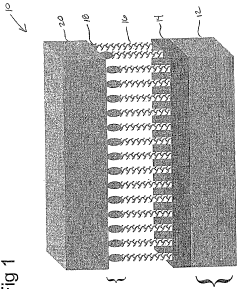
01 Magnetic Tunnel Junction (MTJ) Structures
Magnetic Tunnel Junction structures are fundamental components in spintronic devices, consisting of two ferromagnetic layers separated by an insulating barrier. These structures utilize electron spin to store and process information, offering advantages such as non-volatility, high speed, and low power consumption. Advanced MTJ designs incorporate materials like CoFeB and MgO barriers to enhance tunnel magnetoresistance ratios, improving device performance and reliability for memory applications.- Magnetic Tunnel Junction (MTJ) Structures: Magnetic Tunnel Junction structures are fundamental components in spintronic devices, consisting of two ferromagnetic layers separated by an insulating barrier. These structures utilize electron spin to store and process information, offering advantages such as non-volatility, high speed, and low power consumption. MTJs can be engineered with various materials and configurations to enhance performance characteristics like tunnel magnetoresistance ratio, thermal stability, and switching efficiency.
- Spin-Orbit Torque Devices: Spin-orbit torque (SOT) based spintronic devices utilize the interaction between electron spin and orbital motion to manipulate magnetization. These devices offer advantages in switching speed and energy efficiency compared to conventional spin-transfer torque devices. SOT technology enables the development of advanced memory and logic applications with reduced power consumption and improved reliability, particularly for applications requiring high-speed operation and endurance.
- Integration of Spintronics with Semiconductor Technology: The integration of spintronic elements with conventional semiconductor technology creates hybrid devices that combine the advantages of both fields. These integrated systems enable new functionalities in computing architectures, including non-volatile logic, reconfigurable circuits, and neuromorphic computing applications. The fabrication processes involve compatible materials and structures that can be incorporated into existing CMOS technology platforms while maintaining performance and reliability.
- Novel Materials for Spintronic Applications: Advanced materials play a crucial role in enhancing spintronic device performance. These include topological insulators, Heusler alloys, 2D materials, and various oxide interfaces that exhibit unique spin-dependent transport properties. The development of these materials focuses on improving spin polarization, reducing damping factors, and enhancing spin-orbit coupling effects to create more efficient and versatile spintronic devices with improved thermal stability and reduced critical switching currents.
- Spintronic Sensors and Energy Harvesting Applications: Spintronic technology extends beyond memory and logic to sensing and energy harvesting applications. Spintronic sensors offer high sensitivity for detecting magnetic fields, current, and mechanical motion with advantages in size, power consumption, and compatibility with integrated circuits. Additionally, spin-based thermoelectric and energy conversion devices utilize spin-dependent transport phenomena to convert thermal gradients or electromagnetic radiation into electrical energy, opening new possibilities for energy-efficient systems.
02 Spin-Orbit Torque Devices
Spin-orbit torque (SOT) technology represents a significant advancement in spintronic devices, utilizing the interaction between electron spin and orbital motion to manipulate magnetic states. These devices enable efficient magnetic switching without requiring current flow through the magnetic tunnel junction, resulting in faster operation speeds and reduced energy consumption. SOT-based devices are particularly promising for next-generation memory and logic applications where high endurance and reliability are critical.Expand Specific Solutions03 Integration with Semiconductor Technology
The integration of spintronic devices with conventional semiconductor technology enables the development of hybrid systems that combine the advantages of both technologies. This approach involves fabricating spintronic elements on CMOS platforms, addressing challenges related to material compatibility, thermal budgets, and process integration. Successful integration strategies include back-end-of-line processing techniques and the development of specialized interface layers that preserve the spin-dependent properties while ensuring compatibility with standard semiconductor manufacturing processes.Expand Specific Solutions04 Novel Materials for Spintronics
Advanced materials play a crucial role in enhancing the performance of spintronic devices. These include topological insulators, Heusler alloys, and two-dimensional materials that exhibit unique spin-dependent electronic properties. Research focuses on materials with high spin polarization, low damping constants, and tunable magnetic anisotropy. The development of these novel materials enables spintronic devices with improved efficiency, reduced critical switching currents, and enhanced thermal stability, addressing key challenges in current spintronic technologies.Expand Specific Solutions05 Spintronic Sensing and Computing Applications
Spintronic devices are increasingly being applied in sensing and computing applications beyond traditional memory storage. These include magnetic field sensors with high sensitivity, spin-based logic gates for energy-efficient computing, and neuromorphic computing elements that mimic brain functionality. The unique properties of spin-based devices, such as non-volatility and inherent stochasticity, make them particularly suitable for implementing artificial neural networks and probabilistic computing paradigms, potentially revolutionizing approaches to artificial intelligence and machine learning hardware.Expand Specific Solutions
Key Industry Players in Spintronic Development
The spintronic devices regulatory landscape is evolving within an emerging market characterized by significant growth potential but moderate technological maturity. Currently in the early commercialization phase, the global spintronic market is expanding as applications diversify beyond data storage into computing and sensing. Key industry players demonstrate varying levels of technological readiness: established semiconductor giants like Intel and Micron Technology possess advanced manufacturing capabilities; research-focused entities including CEA, CNRS, and Tohoku University lead fundamental innovation; while specialized companies such as Atomera and Ovonyx focus on specific technological niches. The regulatory framework remains under development, with standards bodies working to address challenges in electromagnetic compatibility, materials safety, and integration with existing semiconductor regulations.
Intel Corp.
Technical Solution: Intel has developed a comprehensive approach to spintronic device regulation, focusing on their MRAM (Magnetoresistive Random Access Memory) technology. Their regulatory strategy includes compliance with international standards such as IEC 62830 for magnetic sensor devices and ISO/IEC 80416 for semiconductor device reliability. Intel has established a dedicated Regulatory Affairs team that works closely with government agencies like the FCC in the US and equivalent bodies in the EU and Asia to ensure their spintronic devices meet electromagnetic compatibility requirements. They've implemented a three-tier compliance framework that addresses material sourcing regulations (including RoHS and REACH compliance), manufacturing process regulations (focusing on environmental impact and worker safety), and end-product regulations (addressing electromagnetic interference and electronic waste disposal). Intel actively participates in industry consortia like the Semiconductor Industry Association to help shape emerging regulations for novel technologies like spintronics.
Strengths: Intel's established presence in semiconductor manufacturing gives them significant regulatory expertise and relationships with regulatory bodies worldwide. Their proactive approach to compliance reduces time-to-market delays. Weaknesses: As a large corporation, Intel faces more regulatory scrutiny than smaller competitors, potentially increasing compliance costs and complexity.
Thales SA
Technical Solution: Thales has pioneered a regulatory approach specifically tailored for defense and aerospace applications of spintronic devices. Their framework addresses the dual-use nature of spintronics technology, which has both civilian and military applications. Thales has developed a proprietary Regulatory Compliance Management System (RCMS) that tracks evolving regulations across multiple jurisdictions, with particular focus on export control regulations such as the Wassenaar Arrangement and ITAR (International Traffic in Arms Regulations). For their spintronic sensors and memory devices, Thales implements enhanced electromagnetic compatibility testing that exceeds standard commercial requirements, meeting military standards like MIL-STD-461 for EMI/EMC. They've established a specialized team that interfaces with defense procurement agencies to ensure their spintronic technologies meet national security requirements while navigating the complex regulatory landscape of classified technologies. Thales also participates in European Defense Agency working groups focused on establishing standards for next-generation electronic components in defense systems.
Strengths: Thales has unparalleled expertise in navigating defense-specific regulations and security requirements for electronic components. Their established relationships with defense procurement agencies provide regulatory insights. Weaknesses: Their focus on defense applications may limit their ability to quickly adapt to commercial regulatory environments, and their compliance processes may add cost and development time.
Core Patents and Innovations in Spintronics
Spin transport electronic device
PatentInactiveUS20170294572A1
Innovation
- A novel electronic device configuration using chiral or helical molecules as a spin selective filter to generate local magnetization in a spin accumulating layer, eliminating the need for static magnets and enabling efficient three-dimensional packaging, data storage, and readout through Hall Effect or giant magneto-resistance measurements.
A spintronic device having a carbon nanotube array-based spacer layer and method of forming same
PatentWO2006022859A2
Innovation
- The development of spintronic devices utilizing arrays of vertically aligned carbon nanotubes as nonmagnetic spacer layers, which allows for large-scale production and maintains high spin coherence, enabling the creation of multilayered hybrid magnetic/CNT devices with ferromagnetic layers acting as spin polarizers and analyzers.
Regulatory Framework and Compliance Requirements
The regulatory landscape for spintronic devices represents a complex and evolving framework that manufacturers, researchers, and developers must navigate. Currently, spintronic technology falls under broader electronic device regulations in most jurisdictions, with few specific standards developed exclusively for this emerging technology. In the United States, the Federal Communications Commission (FCC) and the Consumer Product Safety Commission (CPSC) provide general oversight for electronic devices, while the European Union applies the CE marking requirements through directives such as the Electromagnetic Compatibility Directive (2014/30/EU) and the Restriction of Hazardous Substances (RoHS) Directive (2011/65/EU).
Compliance with materials regulations presents a significant consideration for spintronic device manufacturers. Many spintronic technologies utilize rare earth elements and specialized magnetic materials that may fall under critical materials regulations or conflict minerals reporting requirements. The EU's Registration, Evaluation, Authorization and Restriction of Chemicals (REACH) regulation impacts the manufacturing processes and material selection for these devices, requiring thorough documentation and potential substitution strategies for substances of very high concern (SVHCs).
Data security and privacy regulations increasingly affect spintronic memory devices, particularly as they find applications in data storage systems. The General Data Protection Regulation (GDPR) in Europe and similar frameworks worldwide impose requirements on data storage technologies that spintronic device manufacturers must address through privacy-by-design approaches and enhanced security features.
Export control regulations present another critical compliance area, as spintronic technology may be classified as dual-use technology with potential military applications. The Wassenaar Arrangement, implemented by 42 participating states, establishes controls on exports of dual-use technologies, potentially affecting international collaboration and commercialization pathways for advanced spintronic research and products.
Intellectual property protection forms a crucial component of the regulatory landscape, with patent filings for spintronic technologies increasing dramatically over the past decade. Companies must navigate complex patent landscapes across multiple jurisdictions while ensuring freedom to operate. Standards development organizations like IEEE and JEDEC have begun preliminary work on standardization for certain spintronic applications, though comprehensive standards remain in early development stages.
The regulatory gap between established electronic device frameworks and the unique characteristics of spintronic technologies creates compliance challenges. Industry stakeholders are increasingly engaging with regulatory bodies to develop appropriate frameworks that address the specific properties of spintronic devices while ensuring safety, compatibility, and environmental protection. Proactive regulatory engagement has become a strategic necessity for companies developing commercial spintronic applications.
Environmental and Sustainability Considerations
The environmental and sustainability implications of spintronic devices represent a critical dimension in their regulatory landscape. As these technologies advance toward mainstream adoption, their ecological footprint demands comprehensive assessment. Spintronic devices offer significant energy efficiency advantages over conventional electronics, potentially consuming up to 90% less power during operation due to their non-volatile nature and reduced heat generation.
Material sourcing for spintronic manufacturing presents both challenges and opportunities from a sustainability perspective. Many spintronic technologies rely on rare earth elements and transition metals like cobalt, which raise concerns regarding resource depletion and environmentally damaging extraction practices. Regulatory frameworks increasingly mandate responsible sourcing certifications and supply chain transparency to mitigate these impacts.
End-of-life considerations for spintronic devices are gaining regulatory attention globally. The European Union's Waste Electrical and Electronic Equipment (WEEE) Directive already encompasses emerging technologies, requiring manufacturers to establish recycling protocols before widespread market deployment. Spintronic components present unique recycling challenges due to their complex material compositions, necessitating specialized recovery processes to extract valuable materials while preventing toxic leaching.
Carbon footprint regulations increasingly influence the spintronic industry's development trajectory. Several jurisdictions have implemented carbon pricing mechanisms that incentivize low-emission manufacturing processes. Spintronic device manufacturers must document their products' lifecycle emissions, with some regions requiring carbon neutrality commitments for market access approval.
Water usage in spintronic fabrication facilities faces intensifying scrutiny, particularly in water-stressed regions. Regulatory authorities are implementing progressively stringent water recycling requirements and discharge quality standards. Advanced spintronic manufacturing processes typically require ultra-pure water for production, creating tension between technological advancement and water conservation imperatives.
Chemical management regulations significantly impact spintronic development pathways. The EU's Registration, Evaluation, Authorization and Restriction of Chemicals (REACH) regulation and similar frameworks worldwide restrict hazardous substances in electronic components. Manufacturers must demonstrate compliance through rigorous testing and documentation, potentially limiting certain technical approaches that rely on restricted substances.
Forward-looking regulatory frameworks are beginning to incorporate circular economy principles, requiring spintronic device designers to consider modularity, repairability, and component reusability from inception. These regulations aim to extend product lifecycles and minimize electronic waste, fundamentally reshaping how spintronic technologies are conceptualized and brought to market.
Unlock deeper insights with Patsnap Eureka Quick Research — get a full tech report to explore trends and direct your research. Try now!
Generate Your Research Report Instantly with AI Agent
Supercharge your innovation with Patsnap Eureka AI Agent Platform!