Exploring Spintronic Devices in Nanotechnology Applications
OCT 21, 20259 MIN READ
Generate Your Research Report Instantly with AI Agent
Patsnap Eureka helps you evaluate technical feasibility & market potential.
Spintronics Evolution and Research Objectives
Spintronics represents a revolutionary paradigm in electronics, leveraging the intrinsic spin of electrons alongside their charge to create novel devices with enhanced capabilities. The field emerged in the late 1980s with the discovery of giant magnetoresistance (GMR) by Albert Fert and Peter Grünberg, who were later awarded the 2007 Nobel Prize in Physics for this breakthrough. This discovery marked the beginning of a new era in information technology, enabling significant advancements in data storage density and processing efficiency.
The evolution of spintronics has progressed through several distinct phases. The first generation focused primarily on GMR-based read heads for hard disk drives, dramatically increasing storage capacities. The second generation expanded into magnetic random access memory (MRAM) technologies, offering non-volatile memory solutions with faster access times and lower power consumption compared to conventional semiconductor memories.
Current research is driving the third generation of spintronic devices, which aims to integrate spin-based logic and memory functions into unified architectures. This integration represents a potential solution to the von Neumann bottleneck that limits conventional computing systems, where data transfer between separate processing and memory units creates performance constraints.
The global research landscape in spintronics has seen significant expansion, with major initiatives in the United States, European Union, Japan, China, and South Korea. These efforts are increasingly focused on nanoscale implementations, where quantum effects become more pronounced and exploitable. The convergence of spintronics with nanotechnology has opened new avenues for device miniaturization while maintaining functionality in regimes where conventional electronics face fundamental physical limitations.
Our technical objectives in exploring spintronic devices for nanotechnology applications are multifaceted. First, we aim to develop materials with enhanced spin-orbit coupling properties that can operate efficiently at room temperature, reducing the need for cooling systems that limit practical applications. Second, we seek to design novel device architectures that can effectively manipulate and detect spin states with minimal energy consumption, addressing the growing concern of power efficiency in electronic systems.
Additionally, we intend to investigate integration pathways for spintronic components with existing CMOS technologies, ensuring compatibility with established manufacturing processes. Finally, we will explore emerging applications beyond data storage, including neuromorphic computing systems that mimic brain functionality, quantum computing elements, and ultra-sensitive magnetic field sensors for medical and industrial applications.
Market Analysis for Nanoscale Spintronic Applications
The global market for spintronic devices in nanotechnology applications is experiencing robust growth, driven by increasing demand for high-density data storage solutions and energy-efficient computing systems. Current market valuations indicate that the spintronic technology sector reached approximately 9.1 billion USD in 2022, with projections suggesting a compound annual growth rate (CAGR) of 34% through 2030. This remarkable growth trajectory is primarily fueled by expanding applications in magnetic sensors, magnetic random access memory (MRAM), and hard disk drives (HDDs).
Consumer electronics represents the largest market segment for spintronic applications, accounting for roughly 42% of the total market share. This dominance stems from the integration of spintronic sensors in smartphones, tablets, and wearable devices. The automotive sector follows as the second-largest consumer, with spintronic sensors being increasingly deployed in advanced driver assistance systems (ADAS) and autonomous vehicle technologies.
Geographically, North America currently leads the market with approximately 38% share, benefiting from substantial research investments and the presence of major technology companies. Asia-Pacific is rapidly gaining ground, expected to demonstrate the highest growth rate over the next five years due to expanding manufacturing capabilities in countries like China, South Korea, and Japan.
The enterprise data storage segment presents particularly promising opportunities, as organizations seek more efficient alternatives to conventional memory technologies. MRAM solutions offer significant advantages in terms of power consumption, data retention, and operational speed, making them increasingly attractive for data centers and cloud computing infrastructure.
Healthcare applications represent an emerging market with substantial growth potential. Spintronic biosensors capable of detecting specific biomolecules at extremely low concentrations are revolutionizing diagnostic capabilities, with the medical spintronic device market segment expected to grow at 41% CAGR through 2028.
Key market challenges include high initial manufacturing costs and technical complexities in scaling production. The average cost per unit for spintronic devices remains approximately 2.3 times higher than conventional semiconductor alternatives, creating a significant barrier to widespread adoption in cost-sensitive applications.
Consumer awareness and understanding of spintronic technology benefits remain limited, with market surveys indicating only 23% of potential industrial users fully comprehend the advantages offered by spintronic solutions. This knowledge gap represents both a challenge and an opportunity for market education initiatives.
Current Spintronic Technology Landscape and Barriers
Spintronics technology has evolved significantly over the past two decades, transitioning from theoretical concepts to practical applications. Currently, the global spintronic landscape is characterized by a diverse ecosystem of research institutions, technology companies, and government-funded initiatives. Major research hubs exist in the United States, Europe (particularly Germany and France), Japan, South Korea, and increasingly China, with each region developing specialized expertise in different aspects of spintronic technology.
The current state of spintronic devices encompasses several key technologies including Giant Magnetoresistance (GMR), Tunnel Magnetoresistance (TMR), Spin-Transfer Torque (STT), and emerging Spin-Orbit Torque (SOT) mechanisms. GMR and TMR technologies have already achieved commercial success in hard disk drive read heads and Magnetic Random Access Memory (MRAM), while STT-MRAM is gaining traction as a promising non-volatile memory solution with several commercial products already available from companies like Everspin Technologies and Samsung.
Despite these advances, significant technical barriers impede wider adoption of spintronic devices in nanotechnology applications. A primary challenge is thermal stability at nanoscale dimensions, where maintaining reliable spin states becomes increasingly difficult as device size decreases below 20nm. This challenge is particularly acute for data storage applications requiring long-term data retention. Additionally, current density requirements for spin manipulation remain prohibitively high for many low-power applications, limiting energy efficiency advantages.
Material integration presents another substantial hurdle. Incorporating spintronic materials into conventional CMOS fabrication processes requires overcoming compatibility issues with standard semiconductor manufacturing techniques. The deposition of complex magnetic multilayers with precise thickness control and interface quality demands specialized equipment and processes not widely available in standard semiconductor fabs.
Reliability and endurance issues also persist across spintronic technologies. Write endurance limitations in STT-MRAM devices (typically 10^12 cycles) fall short of requirements for certain cache memory applications. Furthermore, device-to-device variability remains higher than in conventional semiconductor devices, complicating circuit design and potentially reducing yield in manufacturing.
From a manufacturing perspective, scaling production while maintaining consistent magnetic properties presents significant challenges. The precise control of magnetic anisotropy, exchange bias, and interfacial effects becomes increasingly difficult at high-volume production scales, resulting in performance variations that impact overall system reliability.
Addressing these technical barriers requires interdisciplinary approaches combining materials science, device physics, circuit design, and manufacturing engineering. Recent research directions focusing on novel materials like topological insulators, antiferromagnetic materials, and two-dimensional magnetic materials show promise for overcoming some of these limitations, potentially enabling the next generation of spintronic devices for nanotechnology applications.
Contemporary Spintronic Device Architectures
01 Magnetic Tunnel Junction (MTJ) Structures
Magnetic tunnel junctions are fundamental components of spintronic devices, consisting of two ferromagnetic layers separated by an insulating barrier. These structures utilize electron spin to store and process information, offering advantages in non-volatile memory applications. Advanced MTJ designs incorporate materials like MgO barriers and perpendicular magnetic anisotropy to improve performance characteristics such as thermal stability and switching efficiency.- Magnetic Tunnel Junction (MTJ) Based Spintronic Devices: Magnetic Tunnel Junction (MTJ) structures form the foundation of many spintronic devices, utilizing the tunneling magnetoresistance effect. These devices consist of two ferromagnetic layers separated by an insulating barrier, where electron spin determines the resistance state. MTJs are fundamental components in magnetic random access memory (MRAM) and other spintronic applications, offering advantages in non-volatility, energy efficiency, and high-speed operation.
- Spin-Orbit Torque (SOT) Devices: Spin-Orbit Torque (SOT) based spintronic devices utilize the interaction between electron spin and orbital motion to manipulate magnetization. These devices typically employ heavy metals or topological insulators adjacent to ferromagnetic layers to generate spin currents that can efficiently switch magnetic states. SOT devices offer advantages in switching speed, energy efficiency, and reliability compared to conventional spin-transfer torque devices, making them promising for next-generation memory and logic applications.
- Spintronic Sensors and Detectors: Spintronic sensors leverage spin-dependent transport phenomena to detect magnetic fields, current, or other physical quantities with high sensitivity. These devices include magnetic field sensors based on giant magnetoresistance (GMR) or tunneling magnetoresistance (TMR) effects, which are widely used in hard disk drive read heads, biosensors, and industrial sensing applications. The spin-dependent properties enable miniaturization while maintaining high sensitivity and low power consumption.
- Novel Materials for Spintronic Applications: Advanced materials play a crucial role in enhancing spintronic device performance. These include half-metallic ferromagnets, topological insulators, 2D materials like graphene, and various heterostructures that exhibit unique spin-dependent properties. The development of these materials focuses on improving spin polarization, spin coherence length, and spin-orbit coupling to enable more efficient spin injection, transport, and detection in spintronic devices.
- Spintronic Logic and Computing Architectures: Spintronic logic devices utilize electron spin states to perform computational operations, offering potential advantages over conventional CMOS technology in terms of energy efficiency and integration density. These include spin-based logic gates, majority gates, and neuromorphic computing elements that can process information using magnetic domain walls, skyrmions, or other spin textures. Spintronic computing architectures aim to overcome the limitations of conventional electronics by enabling non-volatile computation with reduced energy consumption.
02 Spin-Orbit Torque Devices
Spin-orbit torque (SOT) based spintronic devices utilize the interaction between electron spin and orbital motion to manipulate magnetization. These devices offer advantages in switching speed and energy efficiency compared to conventional spin-transfer torque devices. SOT technology enables the development of high-performance magnetic memory and logic devices with reduced power consumption and improved reliability for next-generation computing applications.Expand Specific Solutions03 Spintronic Sensors and Detectors
Spintronic sensors leverage spin-dependent transport phenomena to detect magnetic fields with high sensitivity. These devices find applications in various fields including data storage, automotive systems, and biomedical sensing. Advanced spintronic sensor designs incorporate novel materials and structures to enhance detection capabilities, improve signal-to-noise ratios, and enable operation in challenging environments.Expand Specific Solutions04 Novel Materials for Spintronics
The development of new materials is crucial for advancing spintronic technology. Materials with unique properties such as high spin polarization, perpendicular magnetic anisotropy, and topological characteristics are being explored. These include Heusler alloys, topological insulators, 2D materials, and various oxide interfaces that exhibit promising spin-dependent transport properties, enabling more efficient and functional spintronic devices.Expand Specific Solutions05 Spintronic Computing Architectures
Spintronic computing architectures leverage the unique properties of electron spin to create novel computational paradigms beyond conventional electronics. These include neuromorphic computing systems that mimic brain functionality, spin-based logic circuits, and quantum computing elements. Such architectures offer potential advantages in energy efficiency, processing speed, and the ability to perform certain computational tasks that are challenging for traditional CMOS-based systems.Expand Specific Solutions
Leading Companies and Research Institutions in Spintronics
Spintronic devices in nanotechnology are currently in the early growth phase, with the market expected to expand significantly as applications in data storage, sensors, and quantum computing mature. The global market is projected to reach several billion dollars by 2030, driven by increasing demand for energy-efficient computing solutions. Leading academic institutions like Tsinghua University, Ohio State University, and Nanyang Technological University are advancing fundamental research, while industry players including Intel, Hitachi, and Thales are focusing on commercialization pathways. Research organizations such as the National Center for Nanoscience & Technology and CEA are bridging the gap between theoretical advances and practical applications. The technology is approaching commercial viability in select applications, though widespread adoption faces challenges in manufacturing scalability and integration with existing semiconductor infrastructure.
Institute of Microelectronics of Chinese Academy of Sciences
Technical Solution: The Institute of Microelectronics of CAS has developed perpendicular magnetic tunnel junction (p-MTJ) technology with diameter scaling below 20nm while maintaining thermal stability factors above 60. Their spintronic devices utilize interface-engineered CoFeB/MgO/CoFeB structures with tungsten insertion layers to enhance perpendicular magnetic anisotropy and reduce critical switching current densities to below 2 MA/cm². The institute has demonstrated functional STT-MRAM arrays with write energies under 100 fJ/bit and read/write speeds below 10ns. Their technology incorporates innovative dual reference layer designs to enhance the tunnel magnetoresistance ratio to over 230% at room temperature. Recent advances include the development of voltage-controlled magnetic anisotropy (VCMA) switching mechanisms that reduce power consumption by approximately 75% compared to conventional spin-transfer torque approaches. The institute has also pioneered the integration of spintronic devices with standard CMOS processes, enabling hybrid memory-logic architectures for in-memory computing applications.
Strengths: Strong materials engineering capabilities; extensive fabrication facilities; integrated approach from materials to devices to systems; significant government funding support; growing patent portfolio. Weaknesses: International collaboration limitations in sensitive technology areas; challenges in commercialization pathways; competition with established memory manufacturers; relatively recent entry into the field compared to some Western and Japanese institutions.
Commissariat à l´énergie atomique et aux énergies Alternatives
Technical Solution: CEA has developed MRAM (Magnetoresistive Random Access Memory) technology based on perpendicular magnetic tunnel junctions (p-MTJs) with thermal stability factors exceeding 80, enabling reliable data retention for over 10 years. Their spintronic devices utilize synthetic antiferromagnetic structures and interface-engineered CoFeB/MgO/CoFeB stacks to achieve tunnel magnetoresistance ratios above 200% at room temperature. CEA has pioneered voltage-controlled magnetic anisotropy (VCMA) switching mechanisms that reduce writing energy by 80% compared to conventional spin-transfer torque approaches. Their technology demonstrates write speeds below 5ns and endurance exceeding 10^12 cycles. CEA has also developed three-terminal spintronic devices incorporating spin-orbit torque (SOT) switching that separates the read and write paths, enabling faster operation and improved reliability. Recent innovations include skyrmion-based racetrack memory concepts for ultra-high-density storage applications.
Strengths: World-leading expertise in materials engineering for spintronics; strong integration with European semiconductor ecosystem; balanced approach addressing both fundamental physics and practical applications; extensive patent portfolio. Weaknesses: Commercialization pathway requires partnerships with semiconductor manufacturers; competing with well-funded Asian and American research programs; challenges in scaling production to industrial levels.
Key Patents and Breakthroughs in Nanoscale Spintronics
Spin-polarized electron source and spin-polarized scanning tunneling microscope
PatentActiveUS7459682B2
Innovation
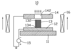
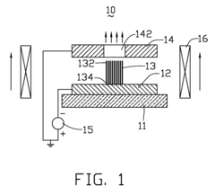
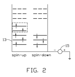
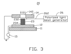
- A spin-polarized electron source utilizing one-dimensional nanostructures of group III-V compound semiconductors with local polarized gap states, where a magnetic field induction or circularly polarized light beam excitation enables efficient spin-polarized electron emission, allowing for continuous and efficient emission of spin-polarized electron currents.
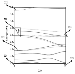
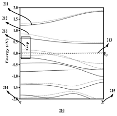
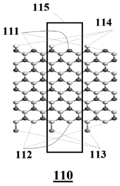
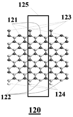
Nanoscale spintronics devices from zn-terminated zigzag boron nitride nanoribbons with giant magnetoresistance effect
PatentActiveIN202131035749A
Innovation
- Zn-terminated zigzag boron nitride nanoribbons (ZBNNRs) are used, with edge termination by zinc, to create nanoscale spintronics devices that exhibit giant magnetoresistance (GMR) effects, enabling ultra-sensitive magnetic field sensors and co-opted intrusion devices through spin-dependent current-voltage characteristics analyzed using DFT-NEGF formalism.
Materials Science Challenges in Spintronic Fabrication
The fabrication of spintronic devices at the nanoscale presents significant materials science challenges that must be overcome to realize their full potential in nanotechnology applications. One of the primary obstacles is achieving precise control over material interfaces, which are critical for spin-dependent transport phenomena. The quality of these interfaces directly impacts spin polarization efficiency and ultimately device performance. Even atomic-level defects or interdiffusion between layers can dramatically reduce spin coherence and transport properties.
Material selection represents another fundamental challenge. While ferromagnetic metals like iron, cobalt, and nickel have been traditional choices, they suffer from limitations in spin coherence length and compatibility with semiconductor processing. Researchers are exploring half-metallic ferromagnets such as Heusler alloys and certain oxides (e.g., Fe3O4, CrO2) that theoretically offer 100% spin polarization, but these materials often fail to maintain their predicted properties when fabricated into actual devices.
Thermal stability poses a significant hurdle, particularly as device dimensions shrink below 20nm. At these scales, superparamagnetic effects become pronounced, potentially causing spontaneous magnetization reversal at room temperature. This necessitates the development of materials with higher magnetic anisotropy while maintaining other desirable spintronic properties.
Scaling challenges are equally problematic. As dimensions decrease, surface and interface effects become increasingly dominant, altering bulk material properties in often unpredictable ways. The ratio of surface atoms to bulk atoms increases dramatically at the nanoscale, leading to modified electronic structures and magnetic behaviors that may not be beneficial for spintronic applications.
Manufacturing consistency presents yet another obstacle. Current fabrication techniques struggle to produce spintronic materials with uniform properties across large wafers, limiting commercial viability. Techniques like molecular beam epitaxy offer excellent control but at prohibitively low throughput, while sputtering methods provide better throughput but often with compromised interface quality.
Novel 2D materials such as graphene and transition metal dichalcogenides show promise for next-generation spintronics due to their unique electronic properties and potentially long spin coherence times. However, integrating these materials with conventional electronics while preserving their desirable properties remains challenging, requiring innovations in transfer techniques and contact engineering to overcome current limitations.
Energy Efficiency Implications of Spintronic Devices
Spintronic devices represent a significant advancement in energy-efficient computing technologies. Unlike conventional electronic devices that rely on electron charge for information processing, spintronic devices utilize electron spin, offering substantial energy savings. Current estimates suggest that spintronic-based memory and logic systems can reduce power consumption by 30-50% compared to traditional CMOS technologies, primarily due to their non-volatile nature which eliminates standby power requirements.
The energy efficiency advantages of spintronics become particularly evident in data storage applications. Magnetic Random Access Memory (MRAM) based on spin transfer torque (STT) or spin-orbit torque (SOT) mechanisms demonstrates remarkably low write energies, typically in the range of 0.1-1 pJ per bit. This represents an order of magnitude improvement over conventional DRAM or flash memory technologies, while maintaining comparable or superior performance metrics.
In computational applications, spintronic devices enable novel computing paradigms such as approximate computing and neuromorphic systems. These approaches inherently trade computational precision for energy efficiency, aligning well with the probabilistic nature of spin-based operations. Preliminary implementations of spintronic-based neural networks have demonstrated energy efficiencies of up to 100 TOPS/W (Tera Operations Per Second per Watt), significantly outperforming conventional digital implementations.
Thermal management represents another critical energy advantage of spintronic technologies. The reduced heat generation in spintronic circuits alleviates cooling requirements, which typically account for 30-40% of data center energy consumption. This cascading effect amplifies the overall energy savings beyond the direct device-level improvements, potentially reducing total system energy requirements by up to 60% in large-scale computing infrastructures.
From a lifecycle perspective, spintronic devices offer additional sustainability benefits. Their non-volatile characteristics extend operational lifetimes, reducing replacement frequency and associated manufacturing energy costs. Furthermore, many spintronic implementations utilize earth-abundant materials like iron and cobalt, reducing the energy-intensive mining and processing required for rare earth elements common in conventional electronics.
However, challenges remain in realizing the full energy efficiency potential of spintronic devices. Current fabrication processes still require high-temperature steps that consume significant energy. Additionally, the integration of spintronic components with conventional CMOS circuitry introduces interface inefficiencies that can partially offset device-level energy gains. Addressing these challenges represents a critical research direction for maximizing the energy benefits of spintronic nanotechnologies.
Unlock deeper insights with Patsnap Eureka Quick Research — get a full tech report to explore trends and direct your research. Try now!
Generate Your Research Report Instantly with AI Agent
Supercharge your innovation with Patsnap Eureka AI Agent Platform!
