

Spintronic Device Standards in Electronics Industry
OCT 21, 202510 MIN READ
Generate Your Research Report Instantly with AI Agent
PatSnap Eureka helps you evaluate technical feasibility & market potential.
Spintronics Evolution and Standardization Goals
Spintronics has evolved significantly since the discovery of giant magnetoresistance (GMR) in the late 1980s by Albert Fert and Peter Grünberg, who were awarded the Nobel Prize in Physics in 2007 for this breakthrough. This discovery marked the beginning of modern spintronics, enabling the manipulation of electron spin as an additional degree of freedom beyond conventional charge-based electronics. The field has progressed through several key phases, from fundamental research to practical applications in data storage technologies, particularly in hard disk drive read heads and magnetic random access memory (MRAM).
The evolution of spintronics has been characterized by increasing integration with conventional semiconductor technologies, moving from discrete components to more complex integrated circuits. This integration has necessitated the development of standardization frameworks to ensure compatibility, reliability, and performance consistency across different manufacturers and applications. Early standardization efforts focused primarily on material specifications and basic measurement protocols for GMR and tunneling magnetoresistance (TMR) devices.
Current standardization goals in spintronics are multifaceted, addressing the needs of an industry transitioning from research to commercial deployment. Primary objectives include establishing uniform testing methodologies for spin-transfer torque (STT) and spin-orbit torque (SOT) devices, defining performance metrics for spintronic memory elements, and creating interoperability standards for spintronic components within conventional CMOS architectures. These standards aim to facilitate broader adoption by providing manufacturers with clear guidelines for production and quality assurance.
Another critical standardization goal involves the development of reference materials and calibration procedures for spintronic measurements, ensuring consistency across research institutions and manufacturing facilities. This includes standardized approaches for characterizing magnetic properties, spin polarization, and spin transport efficiency in various material systems and device geometries.
Looking forward, standardization efforts are increasingly focused on emerging spintronic technologies such as magnonic devices, topological spintronics, and quantum spintronics. These areas require new measurement protocols and performance benchmarks that account for quantum effects and novel spin-based phenomena. Additionally, there is growing recognition of the need for standards addressing the unique reliability and aging characteristics of spintronic devices, which differ significantly from conventional semiconductor components.
International collaboration plays a vital role in these standardization efforts, with organizations such as IEEE, JEDEC, and IEC working alongside industry consortia to develop comprehensive standards. The ultimate goal is to create a robust standardization framework that supports innovation while ensuring the reliability and interoperability necessary for widespread commercial adoption of spintronic technologies across the electronics industry.
Market Demand Analysis for Spintronic Devices
The global market for spintronic devices is experiencing significant growth, driven by increasing demand for high-performance computing, data storage solutions, and energy-efficient electronic components. Current market projections indicate that the spintronic device market will reach approximately $12 billion by 2027, with a compound annual growth rate exceeding 34% from 2022 to 2027. This remarkable growth trajectory reflects the expanding applications of spintronics across multiple industries.
Data storage remains the primary application sector for spintronic technologies, accounting for nearly 60% of the current market share. The demand for higher storage densities and faster access times in data centers continues to drive innovation in magnetic random-access memory (MRAM) and spin-transfer torque magnetic random-access memory (STT-MRAM). Enterprise storage solutions providers are increasingly incorporating these technologies to address the exponential growth in data generation and processing requirements.
The semiconductor industry represents another significant market segment, with major players like Intel, Samsung, and TSMC investing heavily in spintronic research and development. The integration of spintronic components with conventional CMOS technology offers promising solutions for reducing power consumption while maintaining or improving processing capabilities. This aligns perfectly with the industry's push toward more energy-efficient computing architectures.
Consumer electronics manufacturers are also showing growing interest in spintronic technologies, particularly for mobile devices and wearable technology. The non-volatile nature of spintronic memory, combined with its low power consumption characteristics, makes it ideal for extending battery life in portable devices. Market research indicates that consumer applications could represent up to 25% of the spintronic device market by 2025.
Automotive and industrial sectors are emerging as significant growth areas for spintronic applications. Advanced driver-assistance systems (ADAS) and autonomous vehicles require robust, high-performance sensors and memory components that can operate reliably in challenging environments. Similarly, industrial automation systems benefit from the radiation hardness and temperature stability of spintronic devices.
Geographically, North America currently leads the market with approximately 40% share, followed by Asia-Pacific at 35% and Europe at 20%. However, the fastest growth is projected in the Asia-Pacific region, particularly in China, Japan, and South Korea, where substantial investments in semiconductor manufacturing and electronic component development are being made.
The market demand is further bolstered by increasing focus on quantum computing and neuromorphic computing architectures, where spintronic devices offer unique advantages in terms of quantum bit (qubit) implementation and synaptic-like behavior. These emerging computing paradigms represent significant long-term growth opportunities for spintronic technologies.
Current Spintronic Technology Landscape and Challenges
Spintronic technology has evolved significantly over the past two decades, transitioning from theoretical concepts to practical applications in various electronic devices. Currently, the global landscape of spintronics is characterized by rapid advancement in research institutions across North America, Europe, and East Asia, with notable contributions from countries like the United States, Japan, South Korea, and China. Despite this progress, the field faces substantial challenges in standardization, which impedes widespread commercial adoption.
The primary technical challenges in spintronic device standardization include material consistency, manufacturing scalability, and performance reliability. Spintronic materials, particularly those used in magnetic tunnel junctions (MTJs), exhibit significant property variations depending on fabrication conditions, making standardization difficult. The industry currently lacks consensus on testing protocols for key parameters such as spin polarization efficiency, magnetoresistance ratios, and thermal stability.
Manufacturing challenges present another significant barrier. Current production techniques for spintronic devices often involve complex multi-layer deposition processes that are difficult to scale while maintaining consistent performance characteristics. The integration of these devices with conventional CMOS technology requires precise control over interfaces at the nanometer scale, further complicating standardization efforts.
Energy efficiency remains a critical concern in spintronic technology. While theoretically offering lower power consumption than conventional electronics, practical implementations often struggle to achieve the predicted efficiency gains due to issues like high switching currents in spin-transfer torque devices and thermal management challenges in dense arrays.
Reliability testing standards represent another gap in the current landscape. Unlike traditional semiconductor devices with well-established reliability metrics, spintronic devices lack industry-wide agreement on accelerated life testing methodologies, failure mechanisms, and qualification procedures. This absence of standardized reliability frameworks creates uncertainty for potential adopters and manufacturers alike.
The metrology infrastructure for spintronic device characterization also remains underdeveloped. Measurement techniques for quantifying spin-dependent properties often vary between research groups and manufacturers, leading to difficulties in comparing device performance across different platforms and technologies.
International standardization bodies like IEEE and JEDEC have only recently begun addressing spintronic-specific standards, with working groups formed to tackle issues like terminology, measurement methods, and performance specifications. However, these efforts remain in nascent stages compared to the well-established standards for conventional semiconductor technologies.
The fragmented intellectual property landscape further complicates standardization efforts, with key technologies protected by patents held by competing entities. This situation has led to technology silos and hesitancy in collaborative standardization work, as companies seek to protect their competitive advantages in this emerging field.
Current Spintronic Device Standardization Approaches
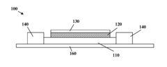
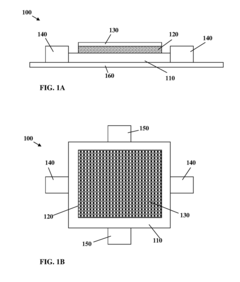
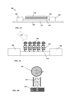
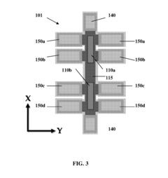
01 Magnetic Tunnel Junction (MTJ) Structures
Magnetic Tunnel Junction structures are fundamental components in spintronic devices, consisting of two ferromagnetic layers separated by an insulating barrier. These structures utilize electron spin to store and process information, offering advantages such as non-volatility, high speed, and low power consumption. Various designs and materials are used to enhance performance characteristics including thermal stability, switching efficiency, and magnetoresistance ratio.- Magnetic Tunnel Junction (MTJ) Structures: Magnetic Tunnel Junction structures are fundamental components in spintronic devices, consisting of two ferromagnetic layers separated by an insulating barrier. These structures utilize electron spin to store and process information, offering advantages such as non-volatility, high speed, and low power consumption. MTJs can be engineered with various materials and configurations to enhance performance characteristics like tunnel magnetoresistance ratio, thermal stability, and switching efficiency.
- Spin Transfer Torque (STT) Technology: Spin Transfer Torque technology enables the manipulation of magnetic states in spintronic devices using spin-polarized currents rather than external magnetic fields. This approach allows for more efficient writing operations in magnetic memory devices and reduces power consumption. STT-based devices can achieve faster switching speeds and higher integration densities, making them suitable for next-generation memory applications such as STT-MRAM (Spin Transfer Torque Magnetic Random Access Memory).
- Novel Materials for Spintronics: Advanced materials play a crucial role in enhancing the performance of spintronic devices. These include half-metallic ferromagnets, topological insulators, 2D materials, and various heterostructures that exhibit unique spin-dependent transport properties. Novel material combinations can improve spin polarization, reduce critical switching currents, enhance thermal stability, and enable new functionalities in spintronic applications. Material engineering at the nanoscale allows for precise control of spin-dependent phenomena.
- Integration with Semiconductor Technology: Integration of spintronic devices with conventional semiconductor technology is essential for practical applications. This involves developing fabrication processes compatible with CMOS technology, addressing interface issues between magnetic and semiconductor materials, and designing appropriate peripheral circuits. Successful integration enables hybrid devices that combine the advantages of both technologies, such as non-volatile logic circuits, reconfigurable computing architectures, and embedded memory solutions.
- Emerging Spintronic Applications: Beyond conventional memory applications, spintronic devices are being developed for various emerging applications. These include neuromorphic computing systems that mimic brain functionality, quantum computing elements utilizing spin qubits, ultra-sensitive magnetic field sensors, energy harvesting devices, and RF/microwave components. These applications leverage unique properties of spin-based devices such as inherent non-linearity, stochasticity, and frequency-dependent behavior to enable new computing paradigms and sensing capabilities.
02 Spin-Orbit Torque (SOT) Based Devices
Spin-Orbit Torque technology represents an advanced approach in spintronic devices where spin current generated through spin-orbit coupling is used to manipulate magnetic states. These devices offer advantages in switching speed and energy efficiency compared to conventional spin-transfer torque devices. SOT-based devices utilize materials with strong spin-orbit coupling to achieve effective spin current generation and magnetic switching without requiring large current densities through the magnetic tunnel junction.Expand Specific Solutions03 Integration with Semiconductor Technology
The integration of spintronic devices with conventional semiconductor technology enables the development of hybrid systems that combine the advantages of both technologies. This integration involves addressing challenges related to material compatibility, fabrication processes, and interface engineering. Approaches include developing CMOS-compatible spintronic devices, creating 3D integration schemes, and designing circuits that effectively utilize the unique properties of spintronic components alongside traditional semiconductor elements.Expand Specific Solutions04 Novel Materials for Spintronics
Advanced materials play a crucial role in enhancing the performance of spintronic devices. These include topological insulators, Weyl semimetals, 2D materials, and various magnetic compounds with unique spin-dependent properties. Research focuses on materials that exhibit high spin polarization, strong spin-orbit coupling, or unusual magnetic ordering to enable new functionalities or improve existing spintronic device performance in terms of energy efficiency, switching speed, and thermal stability.Expand Specific Solutions05 Spintronic Sensors and Memory Applications
Spintronic technology enables the development of highly sensitive magnetic sensors and non-volatile memory devices. These applications leverage the magnetoresistive effects in spintronic structures to detect magnetic fields or store information. Spintronic sensors offer advantages in sensitivity, size, and power consumption compared to conventional sensors, while spintronic memory devices such as MRAM provide non-volatility, high speed, and endurance advantages over traditional memory technologies.Expand Specific Solutions
Key Industry Players in Spintronics Standardization
Spintronic device standards in the electronics industry are evolving within an emerging market characterized by significant growth potential but still developing technical maturity. The industry is transitioning from research to early commercialization, with market projections indicating substantial expansion as applications in memory, sensors, and quantum computing gain traction. Technical development varies across companies, with research institutions like Tohoku University, Tsinghua University, and Ohio State University establishing fundamental principles, while industry leaders including Intel, IBM, and Micron Technology are advancing practical implementations. Thales, Hitachi, and Hon Hai are focusing on specialized applications, creating a competitive landscape where academic-industry partnerships are driving standardization efforts to ensure interoperability and reliability across this promising technology domain.
Intel Corp.
Technical Solution: Intel has developed a comprehensive framework for spintronic device standardization focusing on integration with conventional CMOS technology. Their approach centers on establishing uniform testing protocols for spin-orbit torque (SOT) devices, with particular emphasis on switching current densities (typically 10^11-10^12 A/m²) and thermal stability factors[2]. Intel's standards initiative includes detailed specifications for material interfaces in magnetic tunnel junctions (MTJs), particularly addressing the CoFeB/MgO interface quality metrics that are critical for device performance. They have pioneered reliability testing standards for spintronic devices, establishing endurance benchmarks (>10^15 cycles) and data retention requirements (>10 years at 85°C)[4]. Intel has also been instrumental in developing characterization standards for magnetic damping parameters and spin-transfer efficiency across different material stacks. Their collaboration with equipment manufacturers has resulted in proposed standards for deposition processes of ultra-thin magnetic films with thickness control at the angstrom level, which is essential for reproducible device performance across the industry[7].
Strengths: Intel's standards benefit from their extensive experience in semiconductor manufacturing, ensuring practical implementability. Their approach emphasizes compatibility with existing fabrication infrastructure, lowering barriers to adoption. Weaknesses: Their standards tend to favor CMOS-compatible processes which may limit exploration of more exotic spintronic phenomena. The focus on integration with conventional electronics may constrain more revolutionary applications of spintronics.
Tohoku University
Technical Solution: Tohoku University has established itself as a leading academic institution in spintronic device standardization, particularly through their Spintronics Research Center. Their approach focuses on developing measurement standards for magnetic tunnel junctions (MTJs) with emphasis on tunnel magnetoresistance (TMR) ratios exceeding 600% at room temperature[1]. The university has pioneered standardized testing protocols for spin-transfer torque efficiency in various material systems, creating reference values that are widely cited in academic and industrial research. Their work on perpendicular magnetic anisotropy (PMA) materials has led to proposed standards for thermal stability factors (Δ) and switching current densities in next-generation MRAM devices[3]. Tohoku University researchers have developed comprehensive characterization methods for spin Hall effect materials, establishing standard measurement geometries and analysis techniques that allow for consistent comparison of spin Hall angles across different laboratories. Additionally, they have created reference samples with well-characterized magnetic properties that serve as calibration standards for the spintronic research community[6]. Their collaboration with industry partners has resulted in standardized fabrication processes for MTJ stacks with sub-nanometer precision control.
Strengths: Tohoku University's standards benefit from rigorous academic research and are generally vendor-neutral, encouraging broader industry adoption. Their close collaboration with Japanese electronics manufacturers ensures practical relevance of their proposed standards. Weaknesses: As an academic institution, their standards sometimes emphasize fundamental physics over manufacturing practicality. Implementation of their more advanced characterization techniques often requires specialized equipment not commonly available in production environments.
Critical Patents and Technical Literature in Spintronics
Spin transport electronic device
PatentInactiveUS20170294572A1
Innovation
- A novel electronic device configuration using chiral or helical molecules as a spin selective filter to generate local magnetization in a spin accumulating layer, eliminating the need for static magnets and enabling efficient three-dimensional packaging, data storage, and readout through Hall Effect or giant magneto-resistance measurements.
Strontium oxide as a tunnel barrier for spin injection and giant spin accumulation
PatentActiveUS10134979B1
Innovation
- A spintronic device with a tunnel barrier layer made of strontium oxide (SrO) and a magnetic material layer, which enhances spin injection efficiency by achieving giant spin accumulations and improved spin current magnitude.
International Regulatory Framework for Spintronic Devices
The international regulatory landscape for spintronic devices remains in its developmental stages, with various global bodies working to establish comprehensive frameworks. The International Electrotechnical Commission (IEC) has begun incorporating spintronic technologies into its standardization efforts, particularly through Technical Committee 113, which focuses on nanotechnology standardization. This committee has initiated working groups specifically addressing measurement protocols and characterization methods for spintronic materials and devices.
In the United States, the National Institute of Standards and Technology (NIST) has established the Spintronics Metrology Program, which aims to develop measurement techniques and standards for spintronic devices. This program collaborates with industry partners to ensure that emerging standards meet both scientific rigor and commercial viability requirements. The IEEE Standards Association has also formed interest groups focused on spintronic device integration with conventional CMOS technology.
The European Union, through its European Committee for Electrotechnical Standardization (CENELEC), has launched initiatives to harmonize spintronic device standards across member states. The EU's Horizon Europe program specifically allocates funding for projects aimed at developing standardization frameworks for emerging spintronic technologies, recognizing their potential impact on the European electronics industry.
In Asia, Japan's Industrial Standards Committee (JISC) and China's Standardization Administration (SAC) have both established technical committees focused on spintronic technologies. These bodies are working to develop national standards that align with international frameworks while supporting their domestic industries' competitive positions in the global market.
Safety and environmental considerations form a critical component of the emerging regulatory framework. The Restriction of Hazardous Substances (RoHS) directive and similar regulations worldwide are being evaluated for their applicability to novel materials used in spintronic devices. Particular attention is being paid to rare earth elements and heavy metals that may be present in certain spintronic implementations.
Interoperability standards represent another key focus area, with efforts underway to ensure that spintronic devices can function seamlessly with existing electronic components and systems. This includes standardized interfaces, communication protocols, and performance metrics that enable integration across diverse hardware environments.
The global nature of the electronics supply chain necessitates international coordination in standards development. The World Trade Organization's Technical Barriers to Trade (TBT) Agreement provides a framework for ensuring that technical regulations and standards do not create unnecessary obstacles to international trade, a principle that guides current spintronic standardization efforts.
Interoperability and Integration Challenges
The integration of spintronic devices into existing electronic systems presents significant interoperability challenges that must be addressed through comprehensive standardization efforts. Current electronic systems predominantly rely on CMOS technology, creating compatibility issues when incorporating spintronic components. These challenges manifest at multiple levels - from physical interfaces and signal protocols to power requirements and thermal management considerations.
Signal conversion between conventional charge-based electronics and spin-based devices represents a primary integration hurdle. Spintronic devices operate on fundamentally different principles, requiring specialized interface circuits to translate between spin and charge domains. This translation process often introduces latency and energy overhead, potentially negating some of the inherent advantages of spintronic technology.
Packaging and form factor standardization remains underdeveloped for spintronic components. Unlike mature CMOS technologies with well-established packaging standards, spintronic devices frequently require custom solutions that complicate system-level integration. The lack of standardized footprints and connection schemes increases manufacturing complexity and costs while limiting interchangeability between different vendors' products.
Power management presents another critical challenge. Spintronic devices exhibit unique power profiles that differ significantly from conventional electronics. Current power delivery architectures may require substantial modification to accommodate these differences, particularly for systems incorporating multiple spintronic technologies with varying requirements. Without standardized power interfaces, system designers face increased complexity in energy management.
Data format compatibility issues further complicate integration efforts. Spintronic memory devices often utilize proprietary data structures and addressing schemes that may not align with established memory hierarchies. This necessitates additional translation layers that can impact performance and increase system complexity. Standardized data protocols specifically designed for spintronic characteristics would significantly enhance interoperability.
Testing and validation methodologies for integrated spintronic-CMOS systems remain largely ad hoc. The industry lacks standardized test procedures that can effectively evaluate the performance and reliability of hybrid systems. This gap impedes quality assurance processes and complicates certification for critical applications. Development of comprehensive testing standards represents an essential step toward broader adoption.
Cross-platform software support for spintronic devices remains limited. Operating systems and development environments typically lack native support for spintronic-specific features, requiring custom drivers and middleware solutions. This fragmentation creates barriers for application developers and limits the ecosystem growth necessary for widespread implementation.
Unlock deeper insights with PatSnap Eureka Quick Research — get a full tech report to explore trends and direct your research. Try now!
Generate Your Research Report Instantly with AI Agent
Supercharge your innovation with PatSnap Eureka AI Agent Platform!