The Influence of Spintronic Device Technology on Global Manufacturing Standards
OCT 21, 20259 MIN READ
Generate Your Research Report Instantly with AI Agent
Patsnap Eureka helps you evaluate technical feasibility & market potential.
Spintronic Technology Evolution and Objectives
Spintronics represents a revolutionary paradigm in electronics, leveraging the intrinsic spin of electrons alongside their charge to create novel device functionalities. The evolution of spintronic technology began in the late 1980s with the discovery of giant magnetoresistance (GMR) by Albert Fert and Peter Grünberg, who were subsequently awarded the 2007 Nobel Prize in Physics. This breakthrough enabled the development of highly sensitive magnetic field sensors that dramatically increased data storage densities in hard disk drives, marking the first commercial application of spintronics.
The technological trajectory has since expanded through several key innovations. The transition from GMR to tunnel magnetoresistance (TMR) devices in the early 2000s provided enhanced signal-to-noise ratios and greater sensitivity. Magnetic random-access memory (MRAM) emerged as a promising non-volatile memory technology, combining the speed of SRAM with the persistence of flash memory while consuming significantly less power.
Current research focuses on spin-transfer torque (STT) and spin-orbit torque (SOT) mechanisms, which enable more efficient manipulation of magnetic states using electrical currents. These advancements are crucial for reducing power consumption in spintronic devices, addressing a critical limitation in conventional semiconductor technologies facing thermal dissipation challenges.
The primary objective of spintronic technology development is to establish a new computing paradigm that transcends the limitations of conventional CMOS technology. This includes creating ultra-low-power logic devices, high-density non-volatile memory solutions, and neuromorphic computing architectures that mimic brain functionality. These innovations aim to support the exponential growth in data processing demands while minimizing energy consumption.
Another significant goal is the integration of spintronic components with existing semiconductor manufacturing processes. This compatibility is essential for industrial adoption and scalability, requiring innovations in materials science and fabrication techniques that align with established manufacturing standards.
Looking forward, spintronic technology aims to enable quantum computing applications by utilizing electron spin as quantum bits (qubits). This represents a long-term objective that could revolutionize computational capabilities for specific problem domains. Additionally, researchers are exploring spintronic sensors for biomedical applications and industrial monitoring, expanding the technology's impact beyond traditional computing environments.
The evolution of spintronics is increasingly influenced by global sustainability objectives, with emphasis on developing energy-efficient electronics that reduce the carbon footprint of the rapidly expanding digital infrastructure. This alignment with green technology initiatives represents a strategic direction for spintronic research and development in the coming decades.
Market Demand Analysis for Spintronic Devices
The global market for spintronic devices is experiencing significant growth, driven by increasing demand for high-performance computing, data storage solutions, and energy-efficient electronic components. Current market projections indicate that the spintronic device market will reach approximately $12 billion by 2028, with a compound annual growth rate of 34% from 2023 to 2028. This remarkable growth trajectory reflects the expanding applications of spintronics across multiple industries.
The primary market demand for spintronic devices stems from the data storage sector, where magnetic random-access memory (MRAM) offers substantial advantages over conventional memory technologies. MRAM's non-volatility, high speed, and unlimited endurance address critical limitations in current memory solutions. The semiconductor industry's push toward more energy-efficient components has further accelerated interest in spintronic technologies, as they consume significantly less power than traditional CMOS-based devices.
Manufacturing industries are increasingly seeking spintronic sensors for precision measurement applications, particularly in automotive, aerospace, and industrial automation sectors. These sensors provide enhanced sensitivity, reliability, and performance in harsh environments compared to conventional sensing technologies. The automotive industry alone accounts for approximately 23% of the current spintronic sensor market, with applications in navigation systems, safety features, and engine management.
Healthcare and biomedical applications represent an emerging market segment for spintronic devices, with growing demand for high-sensitivity magnetic biosensors for point-of-care diagnostics and medical imaging. The miniaturization capabilities of spintronic devices align perfectly with the trend toward portable and wearable medical devices, creating substantial market opportunities in this sector.
Geographically, North America and Asia-Pacific regions dominate the spintronic device market, collectively accounting for over 70% of global demand. China, Japan, and South Korea have made substantial investments in spintronic research and manufacturing capabilities, positioning the Asia-Pacific region for the fastest growth rate in the coming years. European markets show increasing adoption rates, particularly in automotive and industrial applications.
The market demand is further shaped by global manufacturing standards, as industries seek components that can meet stringent reliability, performance, and compatibility requirements. This has created a feedback loop where advances in spintronic technology are influencing the development of new manufacturing standards, which in turn drives further innovation and market expansion in spintronic devices.
Global Spintronic Technology Landscape and Barriers
The global spintronic technology landscape has evolved significantly over the past decade, with major research hubs emerging across North America, Europe, and Asia. The United States maintains leadership through substantial investments from DARPA and the National Science Foundation, fostering innovation clusters around universities like MIT, Stanford, and IBM's research facilities. Europe has established strong positions through coordinated EU framework programs, with particularly notable contributions from Germany's Max Planck Institutes and France's Spintec laboratory.
Japan and South Korea have leveraged their semiconductor manufacturing expertise to advance spintronic memory technologies, with companies like Toshiba and Samsung actively developing MRAM solutions. China has rapidly expanded its research capabilities through initiatives like the "Made in China 2025" program, focusing on developing domestic spintronic expertise to reduce technological dependencies.
Despite this global progress, significant barriers impede widespread commercialization of spintronic technologies. Technical challenges remain paramount, including thermal stability issues in nanoscale devices, manufacturing consistency at commercial scales, and integration complexities with existing CMOS technologies. The requirement for ultra-clean fabrication environments and specialized deposition techniques for magnetic multilayers presents substantial manufacturing hurdles.
Economic barriers further complicate advancement, as the high capital investment needed for spintronic manufacturing facilities creates significant market entry barriers. The technology faces a classic "chicken-and-egg" problem: mass production is necessary to reduce costs, but initial high costs limit mass adoption. This economic challenge is particularly acute for startups and smaller research institutions.
Standardization represents another critical barrier, with competing technical approaches and proprietary solutions fragmenting the market. The lack of unified standards for spintronic device characterization, testing protocols, and performance metrics complicates technology evaluation and adoption decisions.
Knowledge barriers also persist, with a limited pool of specialists possessing the interdisciplinary expertise spanning magnetism, electronics, quantum mechanics, and materials science required for spintronic innovation. This talent shortage affects both research advancement and manufacturing implementation.
Regulatory uncertainties surrounding novel materials used in spintronic devices, particularly rare earth elements with complex supply chains, create additional complications. Export controls and intellectual property protection regimes vary significantly across major manufacturing regions, potentially limiting technology transfer and collaborative development opportunities in this strategically important field.
Current Manufacturing Solutions for Spintronic Devices
01 Magnetic Tunnel Junction (MTJ) Devices
Magnetic Tunnel Junction devices are fundamental components in spintronic technology, consisting of two ferromagnetic layers separated by an insulating barrier. These structures utilize electron spin to store and process information, offering advantages in non-volatility and energy efficiency. MTJ-based devices can be used in various applications including magnetic random access memory (MRAM), sensors, and logic devices, providing higher density storage and faster operation compared to conventional electronics.- Magnetic Tunnel Junction (MTJ) Devices: Magnetic Tunnel Junction devices are fundamental components in spintronic technology, utilizing the spin-dependent tunneling effect between ferromagnetic layers separated by an insulating barrier. These structures form the basis for magnetic memory elements, sensors, and logic devices by exploiting the quantum mechanical tunneling of electrons whose probability depends on their spin orientation relative to the magnetization of the ferromagnetic layers.
- Spin Transfer Torque (STT) Technology: Spin Transfer Torque technology enables the manipulation of magnetic states in spintronic devices through the transfer of spin angular momentum from spin-polarized current to local magnetic moments. This mechanism allows for efficient writing operations in magnetic memory devices without requiring external magnetic fields, leading to lower power consumption and improved scalability in memory applications.
- Novel Materials for Spintronic Applications: Advanced materials play a crucial role in enhancing spintronic device performance, including half-metallic ferromagnets, topological insulators, and two-dimensional materials. These materials exhibit unique spin-dependent electronic properties that can significantly improve spin injection efficiency, spin coherence length, and magnetoresistance ratios, enabling the development of more efficient and functional spintronic devices.
- Spintronic Sensors and Detectors: Spintronic-based sensors and detectors leverage the spin-dependent transport properties of electrons to achieve high sensitivity in detecting magnetic fields, electric currents, or radiation. These devices offer advantages such as high spatial resolution, wide dynamic range, and compatibility with standard semiconductor manufacturing processes, making them suitable for applications in data storage, automotive systems, and biomedical imaging.
- Integration of Spintronics with Conventional Electronics: The integration of spintronic devices with conventional CMOS technology represents a significant advancement toward practical applications. This approach combines the non-volatility and energy efficiency of spin-based devices with the high-speed processing capabilities of semiconductor electronics. Hybrid spintronic-CMOS systems enable novel computing architectures, including neuromorphic computing, in-memory processing, and ultra-low-power logic circuits.
02 Spin Transfer Torque (STT) Technology
Spin Transfer Torque technology leverages the transfer of spin angular momentum from spin-polarized current to manipulate the magnetization of ferromagnetic materials. This mechanism enables writing of data in spintronic devices without external magnetic fields, significantly reducing power consumption and increasing scalability. STT-based devices offer improved switching speed and reliability, making them suitable for next-generation memory and computing applications.Expand Specific Solutions03 Spintronic Sensor Applications
Spintronic sensors utilize the spin-dependent transport properties of electrons to detect magnetic fields with high sensitivity and precision. These sensors can be integrated into various systems for applications including position sensing, current monitoring, and biomedical diagnostics. The technology offers advantages such as wide dynamic range, low power consumption, and compatibility with standard semiconductor manufacturing processes, enabling miniaturization and cost-effective production.Expand Specific Solutions04 Novel Materials for Spintronics
Advanced materials play a crucial role in enhancing spintronic device performance. These include half-metallic ferromagnets, topological insulators, 2D materials, and multiferroic compounds that exhibit unique spin-dependent electronic properties. The development of these materials focuses on improving spin polarization, reducing damping, and enhancing thermal stability, which are essential for creating more efficient and reliable spintronic devices with longer lifetimes and better performance characteristics.Expand Specific Solutions05 Spintronic Computing Architectures
Spintronic computing architectures leverage the unique properties of electron spin to create novel computational paradigms beyond conventional electronics. These include neuromorphic computing systems, spin-based logic gates, and quantum computing elements that utilize spin qubits. Such architectures offer potential advantages in terms of processing speed, energy efficiency, and computational density, potentially overcoming the limitations of traditional CMOS-based computing as Moore's Law reaches its physical limits.Expand Specific Solutions
Key Industry Players and Competitive Dynamics
The spintronic device technology market is currently in a growth phase, with an expanding ecosystem of academic institutions and industrial players driving innovation. The global market is projected to reach significant scale as applications in data storage, sensors, and computing gain traction. Leading technology companies like FANUC Corp., Tokyo Electron, and Thales SA are advancing commercial applications, while research institutions including Xidian University, Shanghai Institute of Microsystem & Information Technology, and The Ohio State University are pushing fundamental breakthroughs. The technology maturity varies across applications, with established players like Hitachi Powdered Metals and Minebea Mitsumi focusing on manufacturing standards implementation, while newer entrants like Shanghai Simgui Technology explore emerging spintronic applications, creating a competitive landscape that balances established manufacturing expertise with cutting-edge research.
Tokyo Electron Ltd.
Technical Solution: Tokyo Electron (TEL) has developed specialized deposition and etching equipment specifically optimized for spintronic device manufacturing. Their systems enable precise control of ultra-thin magnetic multilayers required for magnetic tunnel junctions (MTJs), the fundamental building blocks of spintronic devices. TEL's equipment portfolio includes magnetron sputtering systems with in-situ monitoring capabilities that achieve layer thickness control at the sub-nanometer scale, critical for maintaining consistent tunnel magnetoresistance ratios. Their etching solutions address the challenges of patterning magnetic materials without degrading magnetic properties or creating sidewall redeposition issues. TEL has also pioneered integrated annealing systems that enable the crystallization and magnetic property optimization of CoFeB-MgO interfaces, crucial for high-performance MTJs. Their manufacturing standards have been widely adopted across the spintronic industry, particularly for MRAM production.
Strengths: Industry-leading precision in magnetic material deposition; comprehensive equipment ecosystem specifically designed for spintronic manufacturing challenges. Weaknesses: High capital equipment costs; requires specialized expertise for operation and maintenance, limiting accessibility for smaller manufacturers.
Shanghai Institute of Microsystem & Information Technology
Technical Solution: SIMIT has developed comprehensive spintronic device fabrication capabilities focusing on antiferromagnetic spintronics for next-generation memory and logic applications. Their research has yielded significant advances in synthetic antiferromagnets (SAFs) that offer improved thermal stability and reduced stray fields compared to conventional ferromagnetic materials used in spintronic devices. SIMIT's manufacturing approach incorporates specialized deposition techniques for creating precise Ru spacer layers in SAF structures, achieving strong antiferromagnetic coupling essential for stable device operation. They have established testing standards for evaluating spin-orbit torque efficiency in various material systems, contributing to global benchmarking practices for spintronic device performance. SIMIT has also pioneered integration techniques for incorporating spintronic elements with standard CMOS processes, addressing key challenges in signal amplification and readout circuitry for spintronic memory arrays.
Strengths: Leading expertise in antiferromagnetic spintronics; strong government support enabling comprehensive research infrastructure. Weaknesses: Challenges in transitioning from research to commercial-scale manufacturing; international collaboration limitations may affect global standards adoption.
Critical Patents and Technical Innovations
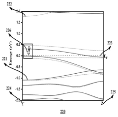
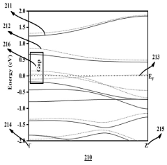
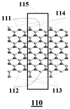
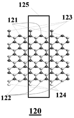
Nanoscale spintronics devices from zn-terminated zigzag boron nitride nanoribbons with giant magnetoresistance effect
PatentActiveIN202131035749A
Innovation
- Zn-terminated zigzag boron nitride nanoribbons (ZBNNRs) are used, with edge termination by zinc, to create nanoscale spintronics devices that exhibit giant magnetoresistance (GMR) effects, enabling ultra-sensitive magnetic field sensors and co-opted intrusion devices through spin-dependent current-voltage characteristics analyzed using DFT-NEGF formalism.
International Standards and Compliance Requirements
The global adoption of spintronic device technology necessitates comprehensive international standards to ensure interoperability, safety, and quality across manufacturing processes. Currently, several key organizations lead standardization efforts in this domain, including the International Electrotechnical Commission (IEC), IEEE Standards Association, and the International Organization for Standardization (ISO). These bodies have established working groups specifically focused on emerging spintronic technologies, addressing both fundamental measurement methodologies and application-specific requirements.
Compliance with these standards presents significant challenges for manufacturers. The unique properties of spintronic devices, particularly their quantum mechanical behavior and sensitivity to magnetic fields, require specialized testing protocols that differ substantially from conventional semiconductor testing. Manufacturers must invest in new measurement equipment capable of characterizing spin polarization, magnetic tunnel junction resistance, and switching characteristics with high precision.
Material composition standards represent another critical compliance area. Spintronic devices utilize complex multilayer structures with precise thickness requirements and specialized magnetic materials. International standards now specify acceptable tolerance ranges for layer thickness variations and compositional uniformity, with particularly stringent requirements for devices intended for medical or aerospace applications.
Environmental considerations have also become increasingly prominent in spintronic manufacturing standards. The rare earth elements and specialized metals used in many spintronic devices face growing regulatory scrutiny. The European Union's Restriction of Hazardous Substances (RoHS) directive and similar regulations worldwide have established specific guidelines for material sourcing, manufacturing waste management, and end-of-life recycling processes for spintronic components.
Reliability testing standards have evolved significantly to address the unique failure mechanisms of spintronic devices. Accelerated life testing protocols now include specialized magnetic field exposure tests, thermal cycling under varying magnetic conditions, and electromigration testing specific to magnetic tunnel junctions. These standards typically require demonstration of device functionality over 10-15 years of simulated operation.
Regional variations in compliance requirements create additional complexity for global manufacturers. While efforts toward harmonization continue, significant differences remain between standards in North America, Europe, and Asia. Japanese standards emphasize reliability metrics, European standards focus on environmental impact, and emerging standards in China prioritize integration with conventional semiconductor manufacturing processes.
The rapid evolution of spintronic technology necessitates regular updates to these standards. Industry consortia and academic research groups actively participate in standards development, ensuring that compliance requirements remain relevant as the technology advances from research laboratories to mass production facilities.
Supply Chain Implications and Material Dependencies
The global spintronic device supply chain represents a complex ecosystem heavily dependent on rare earth elements and specialized materials. Critical materials such as cobalt, tantalum, and rare earth metals like neodymium are essential for manufacturing high-performance spintronic components. These materials often originate from geopolitically sensitive regions, creating significant supply vulnerabilities that manufacturers must navigate through diversification strategies and alternative sourcing approaches.
Material dependencies in spintronic manufacturing have prompted vertical integration efforts among leading manufacturers. Companies are increasingly securing direct access to raw material sources or developing long-term strategic partnerships with suppliers to ensure continuity. This trend is reshaping traditional supplier relationships and creating new power dynamics within the global electronics manufacturing sector.
The specialized nature of spintronic materials has led to the emergence of regional manufacturing clusters with concentrated expertise in material processing and device fabrication. These clusters, primarily located in East Asia, North America, and Western Europe, have developed sophisticated supply networks that support rapid innovation cycles but may also create geographic vulnerabilities in the global supply chain.
Recycling and material recovery processes are becoming increasingly important as manufacturers seek to mitigate supply risks. Advanced recycling technologies specifically designed for spintronic components are being developed to recover valuable materials from end-of-life devices. These circular economy approaches may significantly reduce dependency on primary material sources while addressing environmental concerns associated with electronic waste.
Just-in-time manufacturing practices are being reconsidered in light of spintronic material constraints. Many manufacturers are shifting toward strategic inventory management for critical materials, balancing cost considerations against supply security. This transition is influencing broader manufacturing standards as companies develop new frameworks for material risk assessment and supply chain resilience.
The increasing adoption of spintronic technologies is driving standardization efforts in material specifications and quality control processes. Industry consortia are developing unified testing protocols and material characterization standards to ensure consistency across the supply chain. These emerging standards are facilitating greater interoperability between different manufacturers while establishing baseline quality requirements for spintronic components.
Unlock deeper insights with Patsnap Eureka Quick Research — get a full tech report to explore trends and direct your research. Try now!
Generate Your Research Report Instantly with AI Agent
Supercharge your innovation with Patsnap Eureka AI Agent Platform!