Spintronic Device Technology: Insights into Patent Landscapes
OCT 21, 20259 MIN READ
Generate Your Research Report Instantly with AI Agent
Patsnap Eureka helps you evaluate technical feasibility & market potential.
Spintronics Evolution and Research Objectives
Spintronics represents a revolutionary paradigm in electronic device technology, emerging from the convergence of magnetism and electronics. The field has evolved significantly since the discovery of giant magnetoresistance (GMR) in the late 1980s by Albert Fert and Peter Grünberg, who were subsequently awarded the Nobel Prize in Physics in 2007. This breakthrough marked the beginning of a new era in information technology, enabling the development of higher-density data storage devices and more efficient computing architectures.
The evolution of spintronics has progressed through several distinct phases. The first generation focused primarily on GMR-based read heads for hard disk drives, which dramatically increased storage capacities. The second generation expanded into magnetic tunnel junctions (MTJs) and tunneling magnetoresistance (TMR) effects, enabling the development of magnetic random-access memory (MRAM). Currently, we are witnessing the third generation of spintronic technologies, which explores phenomena such as spin-orbit torque, skyrmions, and topological insulators.
Patent landscapes reveal an accelerating trend in spintronic innovation, with significant growth in patent filings since 2010. Initial patents focused predominantly on fundamental magnetic sensing applications, while recent filings have diversified into neuromorphic computing, quantum information processing, and ultra-low power electronics. This evolution reflects the expanding application potential of spintronic technologies beyond traditional data storage.
Research objectives in the field are increasingly oriented toward addressing critical challenges in modern computing. These include developing non-volatile memory solutions with DRAM-like performance characteristics, creating energy-efficient logic devices that overcome the limitations of CMOS technology, and exploring novel computing paradigms such as probabilistic and neuromorphic computing that leverage the inherent properties of spintronic devices.
The integration of spintronics with other emerging technologies represents another significant research direction. Combining spintronics with 2D materials like graphene and transition metal dichalcogenides offers promising avenues for device miniaturization and performance enhancement. Similarly, the intersection of spintronics with quantum computing could potentially address quantum coherence challenges through topologically protected spin states.
Industry roadmaps suggest that spintronic technologies will play a crucial role in the post-Moore's Law era, offering pathways to continue computational advancement beyond the physical limitations of conventional semiconductor scaling. Research objectives are therefore increasingly focused on demonstrating practical implementations that can compete with or complement existing technologies in terms of performance, energy efficiency, and manufacturing scalability.
Market Analysis for Spintronic Applications
The global market for spintronic applications has witnessed substantial growth in recent years, driven primarily by increasing demand for high-density data storage solutions and energy-efficient electronic devices. The current market size for spintronic technologies is estimated at $5.9 billion, with projections indicating a compound annual growth rate (CAGR) of 34.7% through 2028, potentially reaching $26.8 billion by that time.
Data storage remains the dominant application segment, accounting for approximately 65% of the total market share. This dominance stems from the widespread implementation of Giant Magnetoresistance (GMR) and Tunnel Magnetoresistance (TMR) technologies in hard disk drives and emerging Magnetic Random Access Memory (MRAM) solutions. The MRAM market specifically has shown remarkable growth, expanding at 40% annually as industries seek non-volatile memory alternatives with superior performance characteristics.
Sensor applications represent the second-largest market segment at 18%, with automotive and industrial sectors driving adoption. Spintronic sensors offer advantages in precision, temperature stability, and power efficiency compared to conventional sensing technologies. The automotive industry's shift toward electric vehicles and advanced driver assistance systems has particularly accelerated demand for these specialized sensors.
Emerging application areas showing promising growth include quantum computing, neuromorphic computing, and medical diagnostics. These sectors collectively represent approximately 12% of the current market but are expected to grow significantly faster than traditional segments, with some analysts projecting 50-60% annual growth rates for specialized spintronic quantum computing components.
Geographically, North America leads the market with 38% share, followed by Asia-Pacific (34%) and Europe (22%). However, the fastest growth is occurring in the Asia-Pacific region, particularly in China, Japan, and South Korea, where substantial investments in semiconductor manufacturing and research infrastructure are creating favorable conditions for spintronic technology commercialization.
Key market drivers include increasing data center power consumption concerns, growing demand for IoT devices requiring low-power memory solutions, and the push toward edge computing architectures. Market restraints primarily involve manufacturing complexity, high initial investment requirements, and competition from alternative emerging technologies such as photonics and superconducting electronics.
Consumer electronics represents a particularly promising growth vector, with spintronic components increasingly incorporated into smartphones, wearables, and portable computing devices. Industry analysts project that by 2026, over 40% of premium smartphones will incorporate some form of spintronic technology, primarily in sensor arrays and memory components.
Global Spintronic Technology Status and Barriers
Spintronic technology has witnessed significant advancements globally, yet faces substantial technical and commercial barriers that impede widespread adoption. Current development status varies considerably across regions, with the United States, Japan, and Europe leading research efforts through substantial government funding and established research infrastructure. The U.S. maintains dominance through DARPA-funded initiatives and strong university-industry collaborations at institutions like MIT and Stanford, focusing on MRAM and spin-logic devices.
Japan leverages its historical strength in magnetic materials and electronics manufacturing through companies like Toshiba and Sony, particularly excelling in TMR sensors and STT-MRAM technologies. European research clusters, especially in Germany and France, have made notable contributions to fundamental spintronics theory and novel material development.
China has rapidly accelerated its spintronic research capabilities through national initiatives like the "Made in China 2025" plan, though still lags in fundamental innovation compared to Western counterparts. South Korea, with Samsung and SK Hynix leading efforts, has strategically positioned itself in memory applications of spintronics.
Despite global progress, significant technical barriers persist. Material engineering challenges remain paramount, as creating and maintaining high spin polarization at room temperature continues to be difficult, particularly at interfaces between different materials. Device scaling presents another major hurdle, with spin coherence length limitations restricting miniaturization efforts crucial for commercial viability.
Energy efficiency, while theoretically promising, has not yet reached practical levels for many spintronic applications. Current densities required for spin-transfer torque operations remain too high for mobile applications, limiting market penetration. Manufacturing scalability presents additional challenges, as existing fabrication techniques struggle with the precise atomic-level control needed for reliable spintronic device production.
Integration with conventional CMOS technology represents perhaps the most significant barrier to widespread adoption. The semiconductor industry's established infrastructure is optimized for charge-based electronics, making the incorporation of spin-based components technically complex and economically challenging.
Reliability and operational stability under varying environmental conditions remain concerns for commercial deployment, with temperature sensitivity particularly problematic for automotive and industrial applications. These technical barriers are compounded by market uncertainties and the significant capital investment required to establish new manufacturing paradigms for spintronic devices.
Current Spintronic Device Implementation Approaches
01 Magnetic Tunnel Junction (MTJ) Devices
Magnetic Tunnel Junction (MTJ) devices are fundamental components in spintronic technology, utilizing the spin-dependent tunneling effect between ferromagnetic layers separated by an insulating barrier. These devices form the basis for magnetic random access memory (MRAM) and other spintronic applications. The technology involves manipulating electron spin states to store and process information, offering advantages such as non-volatility, high speed, and low power consumption compared to conventional electronic devices.- Magnetic Tunnel Junction (MTJ) Devices: Magnetic Tunnel Junction (MTJ) devices are fundamental components in spintronic technology, utilizing the spin-dependent tunneling effect between ferromagnetic layers separated by an insulating barrier. These devices form the basis for magnetic random access memory (MRAM) and other spintronic applications. The technology involves manipulating electron spin states to store and process information, offering advantages such as non-volatility, high speed, and low power consumption compared to conventional electronic devices.
- Spin-Transfer Torque (STT) Technology: Spin-Transfer Torque (STT) technology represents an advancement in spintronic devices where the orientation of a magnetic layer can be switched by a spin-polarized current. This mechanism allows for more efficient writing operations in magnetic memory devices without requiring external magnetic fields. STT-based devices offer improved scalability, reduced power consumption, and enhanced performance for data storage and processing applications, making them particularly valuable for next-generation computing architectures.
- Spintronic Sensors and Detectors: Spintronic sensors and detectors leverage the spin-dependent transport properties of electrons to achieve high sensitivity in detecting magnetic fields, current, or other physical parameters. These devices utilize various spintronic effects such as giant magnetoresistance (GMR) or tunneling magnetoresistance (TMR) to convert magnetic signals into electrical outputs. Applications include position sensing, biosensors, automotive sensors, and industrial monitoring systems, offering advantages in terms of sensitivity, size, and power efficiency.
- Spintronic Computing Architectures: Spintronic computing architectures represent novel approaches to information processing that utilize electron spin properties instead of or in addition to conventional charge-based computing. These architectures include spin-based logic gates, neuromorphic computing systems, and quantum computing elements that leverage spin coherence. By utilizing the quantum mechanical properties of electron spin, these technologies aim to overcome the limitations of traditional CMOS-based computing in terms of energy efficiency, processing speed, and integration density.
- Spintronic Memory Integration and Fabrication: Spintronic memory integration and fabrication technologies focus on the methods and processes for incorporating spintronic elements into conventional semiconductor manufacturing flows. This includes techniques for depositing magnetic materials, patterning nanoscale spintronic structures, and integrating them with CMOS circuitry. Advanced fabrication approaches address challenges related to thermal stability, interface quality, and scalability, enabling the mass production of spintronic devices with consistent performance characteristics for commercial applications.
02 Spin-Transfer Torque (STT) Technology
Spin-Transfer Torque (STT) technology represents an advancement in spintronic devices where the orientation of a magnetic layer can be switched using a spin-polarized current. This mechanism allows for more efficient writing operations in magnetic memory devices without requiring external magnetic fields. STT-based devices offer improved scalability, reduced power consumption, and enhanced reliability for data storage and processing applications in next-generation computing systems.Expand Specific Solutions03 Spintronic Sensors and Detectors
Spintronic sensors and detectors leverage the spin properties of electrons to achieve high sensitivity in measuring magnetic fields, current, or other physical parameters. These devices utilize phenomena such as giant magnetoresistance (GMR) or tunneling magnetoresistance (TMR) to convert magnetic signals into electrical outputs. Applications include position sensing, biosensors, automotive systems, and industrial monitoring, offering advantages in terms of sensitivity, size, and power efficiency compared to conventional sensing technologies.Expand Specific Solutions04 Spintronic Logic and Computing Devices
Spintronic logic and computing devices utilize electron spin states to perform computational operations, potentially overcoming limitations of conventional CMOS technology. These devices implement logic functions through spin-based phenomena, enabling novel computing architectures such as non-volatile logic, neuromorphic computing, and quantum-inspired systems. The technology promises significant advantages in terms of energy efficiency, processing speed, and integration density for future computing paradigms.Expand Specific Solutions05 Spintronic Data Storage Systems
Spintronic data storage systems utilize electron spin properties to store information, offering advantages over conventional storage technologies. These systems include various implementations of magnetic random access memory (MRAM), racetrack memory, and other spin-based storage concepts. The technology provides non-volatility, high speed, unlimited endurance, and radiation hardness, making it suitable for applications ranging from consumer electronics to aerospace and defense systems where reliability and performance are critical.Expand Specific Solutions
Leading Companies and Research Institutions in Spintronics
The spintronic device technology market is currently in a growth phase, characterized by increasing research intensity and patent activity. The global market size is projected to expand significantly as applications in data storage, sensors, and quantum computing gain traction. From a technological maturity perspective, the field shows varied development levels across applications, with major players driving innovation through different approaches. Samsung Electronics and Intel lead in commercial applications, while IBM demonstrates strength in fundamental research. Academic institutions like MIT and specialized research entities such as Yeda Research & Development contribute significant intellectual property. Companies like Texas Instruments and Apple are strategically positioning themselves in this space, focusing on integration possibilities with existing semiconductor technologies.
Samsung Electronics Co., Ltd.
Technical Solution: Samsung has developed a comprehensive spintronic technology platform centered around STT-MRAM for both standalone and embedded memory applications. Their technical approach focuses on optimizing the magnetic tunnel junction (MTJ) stack structure to achieve the optimal balance between thermal stability, switching current, and reliability. Samsung has successfully demonstrated 28nm embedded MRAM technology with endurance exceeding 10^12 cycles and data retention of over 10 years at 125°C. Their patented solutions include specialized synthetic antiferromagnetic reference layers that enhance stability against external magnetic fields while maintaining high tunnel magnetoresistance ratios. Samsung has also pioneered integration techniques for incorporating spintronic devices into standard CMOS back-end-of-line processes, enabling cost-effective manufacturing. Recent developments include voltage-controlled magnetic anisotropy (VCMA) approaches that significantly reduce power consumption during write operations, addressing a key limitation of conventional STT-MRAM technology. Their patent portfolio also covers specialized sensing circuits designed to operate with the unique characteristics of spintronic devices.
Strengths: Samsung possesses end-to-end capabilities from materials research through high-volume manufacturing, allowing them to rapidly commercialize spintronic innovations. Their extensive experience in memory technologies provides valuable insights for market-ready implementations. Weaknesses: Their focus appears more concentrated on memory applications rather than logic or neuromorphic computing, potentially limiting their impact in emerging spintronic application areas beyond storage.
Intel Corp.
Technical Solution: Intel has developed a sophisticated spintronic technology platform primarily focused on embedded MRAM solutions for cache and non-volatile memory applications. Their technical approach centers on perpendicular magnetic tunnel junctions (p-MTJs) with engineered CoFeB-MgO interfaces that provide high tunnel magnetoresistance while maintaining thermal stability. Intel's patented designs include specialized synthetic antiferromagnetic structures that enhance resistance to external magnetic fields while reducing device-to-device variations. Their process integration techniques have successfully demonstrated 22nm FinFET-compatible MRAM with write endurance exceeding 10^6 cycles and retention times suitable for persistent memory applications. Intel has also pioneered circuit-level innovations including specialized sense amplifiers that accommodate the unique resistance characteristics of MTJ devices, enabling reliable read operations with minimal power consumption. Recent patents reveal development in spin-orbit torque (SOT) based devices that separate read and write paths, potentially enabling faster switching speeds and reduced write energy compared to conventional STT-MRAM approaches. Their technology roadmap includes integration of spintronic devices with advanced logic nodes below 10nm.
Strengths: Intel's extensive experience in logic process technology provides unique advantages for tight integration of spintronic devices with advanced computing architectures. Their comprehensive approach spans materials, devices, circuits, and system architecture. Weaknesses: Their solutions appear primarily focused on memory applications rather than logic replacement, potentially limiting the transformative impact of their spintronic portfolio on computing paradigms beyond conventional von Neumann architectures.
Key Patents and Technical Innovations in Spintronics
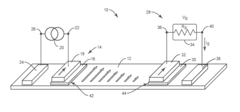
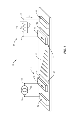
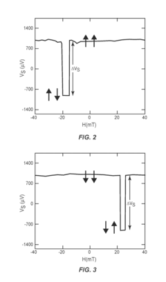
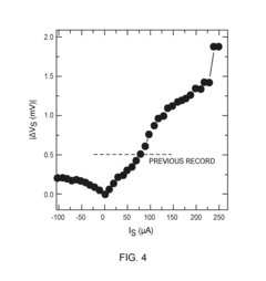
Strontium oxide as a tunnel barrier for spin injection and giant spin accumulation
PatentActiveUS10134979B1
Innovation
- A spintronic device with a tunnel barrier layer made of strontium oxide (SrO) and a magnetic material layer, which enhances spin injection efficiency by achieving giant spin accumulations and improved spin current magnitude.
Patent Landscape Analysis Methodology
The patent landscape analysis methodology for spintronic device technology requires a systematic approach to extract meaningful insights from patent data. This methodology typically begins with the definition of search parameters, including key terms related to spintronic technologies such as magnetic tunnel junctions, spin-transfer torque, and spin-orbit torque. These parameters are crucial for ensuring comprehensive coverage while maintaining relevance to the specific technological domain.
Database selection constitutes the next critical step, with options ranging from specialized patent databases like Derwent Innovation and PatBase to free resources such as Google Patents and the USPTO database. For spintronic technology, databases with strong coverage of Asian patents are particularly valuable, given the significant research activities in Japan, South Korea, and China.
The extraction and cleaning of patent data follows, involving the collection of bibliographic information, abstracts, claims, and full specifications. This process often employs automated tools to handle large datasets, followed by manual verification to ensure data integrity. For spintronic patents, particular attention must be paid to technical terminology and classification codes specific to magnetic and electronic device technologies.
Quantitative analysis techniques form the backbone of patent landscape assessment, including trend analysis to track filing patterns over time, geographical distribution analysis to identify innovation hubs, and assignee analysis to map key players in the spintronic ecosystem. These analyses often reveal technology development cycles and competitive positioning within the industry.
Qualitative assessment complements the quantitative approach by examining claim scope, citation networks, and technological significance. For spintronic devices, this might involve evaluating patents based on their potential impact on data storage density, energy efficiency, or processing speed improvements.
Visualization tools transform complex patent data into interpretable formats, such as heat maps showing technology concentration, network diagrams illustrating relationships between patent holders, and timeline charts depicting technology evolution. These visualizations are particularly effective for communicating spintronic technology trends to non-technical stakeholders.
The final component involves interpretation and strategic recommendation, where patent landscape findings are translated into actionable business intelligence, identifying white spaces for innovation, potential licensing opportunities, and freedom-to-operate considerations in the rapidly evolving field of spintronic devices.
Intellectual Property Strategy for Spintronic Technologies
Developing a comprehensive intellectual property strategy is crucial for companies investing in spintronic technologies. The patent landscape in this field has grown exponentially over the past decade, with major technology companies and research institutions securing key innovations. Strategic IP management requires a multi-faceted approach that balances protection and commercialization opportunities.
Patent filing strategies should focus on both core technology patents and application-specific implementations. Companies should prioritize securing fundamental patents covering novel materials, device structures, and manufacturing processes that enable spintronic functionality. These cornerstone patents provide broad protection and significant licensing potential. Simultaneously, application patents targeting specific use cases in memory, sensing, and logic applications create valuable defensive portfolios.
Geographic considerations play a vital role in spintronic IP strategy. While the United States, Japan, and Europe remain primary patent filing destinations, China has emerged as a critical jurisdiction due to its growing manufacturing capabilities and domestic market. Strategic patent families should cover these key regions to maximize protection and commercial leverage.
Licensing and partnership frameworks represent another essential component of spintronic IP strategy. Cross-licensing agreements with complementary technology holders can overcome patent thickets that might otherwise impede commercialization. University partnerships offer access to cutting-edge research and early-stage innovations, while industry consortia facilitate standard-setting and shared risk in pre-competitive research.
Freedom-to-operate analyses must be conducted regularly as the spintronic patent landscape evolves rapidly. Companies should maintain vigilant monitoring of competitor patent activities, particularly around MRAM, spin-orbit torque devices, and spintronic logic implementations. Defensive publication strategies can be employed for incremental innovations that may not warrant full patent protection but should remain in the public domain.
Trade secret protection complements patent strategies, particularly for manufacturing processes and material formulations that are difficult to reverse-engineer. Companies must implement robust internal controls to safeguard these valuable unpatented innovations while maximizing their competitive advantage.
Finally, IP valuation methodologies specific to spintronic technologies should be developed to accurately assess portfolio strength and guide investment decisions. These valuations should consider not only current applications but also future potential as spintronic devices continue to evolve and find new applications across computing, automotive, IoT, and other emerging sectors.
Unlock deeper insights with Patsnap Eureka Quick Research — get a full tech report to explore trends and direct your research. Try now!
Generate Your Research Report Instantly with AI Agent
Supercharge your innovation with Patsnap Eureka AI Agent Platform!