

Material Innovations in Spintronic Device Development for Smart Cities
OCT 21, 202510 MIN READ
Generate Your Research Report Instantly with AI Agent
PatSnap Eureka helps you evaluate technical feasibility & market potential.
Spintronics Background and Innovation Goals
Spintronics emerged in the late 1980s with the discovery of giant magnetoresistance (GMR) by Albert Fert and Peter Grünberg, who were later awarded the Nobel Prize in Physics for this breakthrough. This phenomenon, where electrical resistance changes significantly in response to magnetic fields, laid the foundation for modern data storage technologies. Over the past three decades, spintronics has evolved from a theoretical concept to a practical technology with applications spanning from hard disk drives to emerging quantum computing systems.
The technological evolution of spintronics has been marked by several key milestones, including the development of magnetic tunnel junctions (MTJs), spin-transfer torque (STT) mechanisms, and more recently, spin-orbit torque (SOT) devices. Each advancement has progressively improved energy efficiency, switching speed, and integration capabilities, making spintronic devices increasingly viable for commercial applications beyond traditional data storage.
In the context of smart cities, spintronic technology presents unique opportunities due to its inherent advantages of non-volatility, low power consumption, and high-speed operation. These characteristics align perfectly with the demands of distributed sensor networks, edge computing devices, and IoT infrastructure that form the backbone of smart urban environments. The ability to maintain state without continuous power input makes spintronic devices particularly valuable for energy-constrained applications in urban settings.
The primary innovation goals for spintronic materials in smart city applications center around three critical areas. First, developing materials with enhanced spin-orbit coupling properties to improve energy efficiency and reduce the power requirements of edge devices deployed throughout urban infrastructure. Second, creating more robust spintronic materials capable of operating reliably in varied environmental conditions encountered in urban settings, from temperature fluctuations to electromagnetic interference. Third, scaling production techniques to enable cost-effective mass manufacturing of spintronic components for widespread deployment.
Recent advances in two-dimensional materials, particularly transition metal dichalcogenides and topological insulators, have opened new avenues for spintronic innovation. These materials exhibit unique spin-dependent properties that could potentially overcome current limitations in conventional spintronic devices. The integration of these novel materials with existing silicon-based technologies represents a crucial technical objective for enabling practical smart city applications.
The convergence of spintronics with other emerging technologies, such as neuromorphic computing and artificial intelligence, further expands the potential impact on smart city infrastructure. Spintronic-based neuromorphic systems could enable energy-efficient, real-time data processing at the edge, significantly reducing the bandwidth requirements for urban sensor networks while enhancing privacy through localized data processing.
Smart City Market Demand for Spintronic Solutions
The smart city market is experiencing unprecedented growth, with projections indicating a global valuation exceeding $2.5 trillion by 2025. Within this expanding ecosystem, spintronic solutions are emerging as critical enablers for next-generation urban infrastructure. Market research reveals increasing demand for energy-efficient computing systems that can process massive data streams generated by urban sensors and IoT networks while consuming minimal power.
Smart city administrators and technology providers are actively seeking alternatives to conventional semiconductor technologies that face fundamental physical limitations in power efficiency. Spintronics, leveraging electron spin rather than charge, presents a compelling solution to this challenge, with potential energy savings of 70-90% compared to traditional CMOS technologies in specific applications.
The demand for spintronic solutions in smart cities is primarily driven by four key application domains. First, transportation management systems require edge computing capabilities that can process sensor data with minimal latency and power consumption. Second, energy grid optimization demands distributed intelligence that can operate reliably under variable environmental conditions. Third, public safety and surveillance networks need robust data processing capabilities that can function continuously with minimal maintenance. Fourth, environmental monitoring systems require sensors and processors that can operate on harvested energy in remote locations.
Market surveys indicate that municipal decision-makers prioritize technology solutions with extended operational lifespans, reduced maintenance requirements, and lower total cost of ownership. Spintronic devices, with their inherent non-volatility and reduced heat generation, align perfectly with these priorities, potentially extending hardware replacement cycles by 30-50%.
The integration of artificial intelligence into urban management systems is accelerating demand for specialized computing architectures. Neuromorphic computing approaches based on spintronic materials show particular promise for pattern recognition and anomaly detection in urban environments, with market adoption expected to grow at 35% annually through 2030.
Regional analysis reveals differentiated market needs, with established urban centers in Europe and North America focusing on retrofitting existing infrastructure with more efficient technologies, while rapidly developing cities in Asia prioritize scalable solutions that can grow with expanding urban populations. This geographic diversity in market requirements necessitates adaptable spintronic device designs that can be customized for specific deployment scenarios.
Industry partnerships between material science companies, device manufacturers, and urban technology integrators are forming to address this emerging market opportunity, with several pilot projects demonstrating the feasibility of spintronic solutions in real-world smart city applications.
Current Challenges in Spintronic Material Development
Despite significant advancements in spintronics over the past decade, material development remains a critical bottleneck in the widespread implementation of spintronic devices for smart city applications. The primary challenge lies in developing materials that can maintain spin coherence at room temperature while being compatible with existing semiconductor manufacturing processes. Current spintronic materials often exhibit excellent performance only at extremely low temperatures, making them impractical for real-world smart city deployments.
Material stability presents another significant hurdle. Many promising spintronic materials degrade rapidly when exposed to environmental factors such as humidity, temperature fluctuations, and oxidation—conditions that are unavoidable in smart city infrastructure. This degradation significantly reduces device lifespan and reliability, making them unsuitable for long-term deployment in critical urban systems.
Scalability of material production represents a substantial challenge for industrial adoption. While laboratory-scale synthesis of novel spintronic materials has shown promising results, translating these processes to industrial-scale production while maintaining consistent material properties has proven difficult. The precision required for spintronic material fabrication often involves complex deposition techniques that are difficult to scale without compromising quality.
Interface engineering between different materials in spintronic devices remains problematic. The performance of spintronic devices critically depends on the quality of interfaces between ferromagnetic and non-magnetic layers. Atomic-level control of these interfaces is necessary but challenging to achieve consistently in manufacturing environments, leading to device-to-device variations that hamper reliability in smart city applications.
Energy efficiency constraints pose another significant challenge. While spintronics promises lower power consumption compared to conventional electronics, current materials still require substantial energy for spin manipulation, particularly for writing operations. This limitation reduces the potential energy savings in large-scale smart city deployments where power efficiency is paramount.
Rare earth element dependency creates supply chain vulnerabilities. Many high-performance spintronic materials rely on rare earth elements that face supply constraints and geopolitical complications. This dependency raises concerns about the long-term sustainability and cost-effectiveness of spintronic solutions for smart cities, particularly as demand scales.
Integration with existing CMOS technology remains challenging due to material compatibility issues. The thermal budget constraints of CMOS back-end processing limit the types of materials and processes that can be used for spintronic device fabrication, restricting design options and potentially compromising performance in integrated systems.
Current Material Solutions for Spintronic Devices
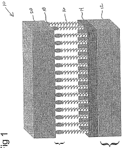
01 Magnetic Tunnel Junction (MTJ) Based Spintronic Devices
Magnetic Tunnel Junction (MTJ) structures are fundamental components in spintronic devices, consisting of two ferromagnetic layers separated by a thin insulating barrier. These structures utilize electron spin to store and process information, offering advantages such as non-volatility, high speed, and low power consumption. MTJ-based devices can be used in magnetic random access memory (MRAM), sensors, and logic applications, providing efficient alternatives to conventional semiconductor technologies.- Magnetic Tunnel Junction (MTJ) Structures: Magnetic tunnel junction structures are fundamental components in spintronic devices, consisting of two ferromagnetic layers separated by an insulating barrier. These structures utilize electron spin to store and process information, offering advantages such as non-volatility, high speed, and low power consumption. Various designs and materials are employed to enhance performance characteristics including tunnel magnetoresistance ratio, thermal stability, and switching efficiency.
- Spin-Orbit Torque Devices: Spin-orbit torque (SOT) based spintronic devices utilize the interaction between electron spin and orbital motion to manipulate magnetization. These devices offer advantages in switching speed and energy efficiency compared to conventional spin-transfer torque mechanisms. SOT devices typically incorporate heavy metal layers adjacent to ferromagnetic materials to generate the necessary spin currents for magnetization switching, enabling applications in memory, logic, and sensing technologies.
- Integration with Semiconductor Technology: The integration of spintronic devices with conventional semiconductor technology enables hybrid systems that combine the advantages of both platforms. This approach addresses challenges in fabrication compatibility, signal conversion, and system architecture. Integration methods include monolithic fabrication on silicon substrates, 3D stacking, and development of interface circuits that efficiently translate between charge-based and spin-based information processing paradigms.
- Novel Materials for Spintronics: Advanced materials play a crucial role in enhancing spintronic device performance. These include topological insulators, Weyl semimetals, 2D materials, and various heterostructures that exhibit unique spin-dependent transport properties. Material engineering focuses on improving spin polarization, reducing damping constants, enhancing spin-orbit coupling, and maintaining desirable properties at room temperature to enable practical applications in computing and data storage.
- Spintronic Sensing and Detection Applications: Spintronic devices offer unique capabilities for sensing and detection applications due to their sensitivity to magnetic fields, temperature, and other physical parameters. These applications include magnetic field sensors, biosensors, position detectors, and current monitoring systems. The inherent advantages of spintronic sensors include high sensitivity, wide dynamic range, miniaturization potential, and compatibility with integrated circuit technology, making them suitable for IoT devices and biomedical applications.
02 Spin-Orbit Torque (SOT) Devices
Spin-Orbit Torque (SOT) devices leverage the interaction between electron spin and orbital motion to manipulate magnetic states. These devices utilize materials with strong spin-orbit coupling to generate torques that can switch magnetic layers efficiently. SOT-based spintronic devices offer advantages including faster switching speeds, reduced energy consumption, and improved reliability compared to conventional spin-transfer torque devices, making them promising candidates for next-generation memory and computing applications.Expand Specific Solutions03 Spintronic Sensors and Detectors
Spintronic sensors utilize the spin-dependent transport properties of electrons to detect magnetic fields with high sensitivity. These devices can be designed for various applications including position sensing, current monitoring, and biomedical diagnostics. By leveraging phenomena such as giant magnetoresistance (GMR) or tunneling magnetoresistance (TMR), spintronic sensors offer advantages including high spatial resolution, wide dynamic range, and compatibility with standard semiconductor manufacturing processes.Expand Specific Solutions04 Novel Materials for Spintronic Applications
Advanced materials play a crucial role in enhancing the performance of spintronic devices. These include half-metallic ferromagnets, topological insulators, 2D materials, and various heterostructures that exhibit unique spin-dependent properties. The development of these materials focuses on achieving high spin polarization, long spin coherence times, and efficient spin-charge conversion. Novel deposition techniques and nanofabrication methods are employed to create these materials with precise control over their structural and magnetic properties.Expand Specific Solutions05 Spintronic Logic and Computing Architectures
Spintronic logic devices utilize electron spin states to perform computational operations, offering potential advantages over conventional CMOS technology. These include non-volatile operation, reduced power consumption, and the ability to combine memory and logic functions. Various spintronic logic architectures have been proposed, including majority gates, spin wave devices, and domain wall logic. These approaches aim to overcome the limitations of traditional computing paradigms by exploiting the quantum mechanical properties of electron spin.Expand Specific Solutions
Leading Companies and Research Institutions in Spintronics
The spintronic device development for smart cities market is currently in its growth phase, with significant research momentum but limited commercial deployment. The global market is projected to reach approximately $2-3 billion by 2025, driven by increasing demand for energy-efficient computing solutions. From a technological maturity perspective, the landscape features a mix of established players and research institutions. Intel and Western Digital are leveraging their semiconductor expertise to commercialize spintronic memory solutions, while Thales and Hitachi are developing specialized applications for smart infrastructure. Academic institutions like MIT, Ohio State University, and Chinese Academy of Sciences are pioneering fundamental research, with Yeda Research and Yissum Research Development commercializing university innovations. Interuniversitair Micro-Electronica Centrum (IMEC) serves as a crucial bridge between academic research and industrial applications, accelerating technology transfer in this emerging field.
Intel Corp.
Technical Solution: Intel has developed advanced spintronic memory solutions specifically designed for smart city applications. Their Magnetoresistive Random Access Memory (MRAM) technology utilizes spin-transfer torque (STT) mechanisms to create non-volatile memory cells with significantly lower power consumption compared to traditional SRAM/DRAM solutions. Intel's spintronic devices feature perpendicular magnetic anisotropy (PMA) materials that enable higher density storage while maintaining thermal stability. For smart city implementations, Intel has integrated these spintronic components with their IoT platforms, creating edge computing solutions that can process sensor data with minimal power requirements. Their recent developments include specialized spintronic sensors capable of detecting magnetic field variations in urban environments, useful for traffic monitoring and infrastructure assessment applications. Intel has also pioneered the integration of spintronic logic elements with CMOS technology, creating hybrid computing architectures optimized for the distributed processing needs of smart city networks.
Strengths: Intel's extensive manufacturing infrastructure allows for large-scale production of spintronic devices with consistent quality. Their integration capabilities with existing semiconductor technologies create practical implementation pathways. Weaknesses: Their spintronic solutions still face challenges in achieving the write speeds necessary for real-time smart city applications, and the technology requires specialized fabrication processes that increase production costs.
Tohoku University
Technical Solution: Tohoku University has pioneered breakthrough material innovations in spintronic device development specifically targeting smart city applications. Their research team has developed novel half-metallic Heusler alloys (Co2MnSi and Co2FeSi) that demonstrate nearly 100% spin polarization at room temperature, a critical advancement for energy-efficient spintronic devices. These materials have been incorporated into magnetic tunnel junctions with record-high magnetoresistance ratios exceeding 600% at room temperature. For smart city applications, Tohoku has created ultra-sensitive spintronic sensor arrays capable of detecting minute magnetic field changes, enabling applications from traffic monitoring to structural health assessment of urban infrastructure. Their innovation in perpendicular magnetic anisotropy materials has led to spintronic memory elements with data retention exceeding 10 years while requiring minimal power for state switching. Tohoku's researchers have also developed specialized spintronic neuromorphic computing elements that mimic synaptic functions, creating energy-efficient edge computing solutions for distributed smart city sensor networks. Their recent work includes the integration of these spintronic elements with flexible substrates, enabling conformable sensors that can be applied to curved urban infrastructure surfaces.
Strengths: Tohoku University maintains world-leading expertise in fundamental spintronics materials science, consistently producing materials with superior spin transport properties. Their close collaboration with Japanese electronics manufacturers creates clear pathways to commercialization. Weaknesses: Some of their most advanced materials require specialized deposition techniques that are challenging to scale to industrial production, and their neuromorphic computing implementations are still in early research stages.
Key Patents and Breakthroughs in Spintronic Materials
Spintronic materials and spintronic devices including the spintronic materials
PatentInactiveUS20160222039A1
Innovation
- The development of halide perovskite materials, which are formed by dissolving RX and MX2 in a solvent, deposited onto a substrate, and then heated to form a film, allowing for spintronic devices that can be driven by both photons and electrons, with strong spin-orbit coupling and tunable properties.


A spintronic device having a carbon nanotube array-based spacer layer and method of forming same
PatentWO2006022859A2
Innovation
- The development of spintronic devices utilizing arrays of vertically aligned carbon nanotubes as nonmagnetic spacer layers, which allows for large-scale production and maintains high spin coherence, enabling the creation of multilayered hybrid magnetic/CNT devices with ferromagnetic layers acting as spin polarizers and analyzers.
Energy Efficiency and Sustainability Considerations
The integration of spintronics technology into smart city infrastructure presents significant opportunities for enhancing energy efficiency and sustainability. Spintronic devices fundamentally operate on electron spin rather than charge, enabling lower power consumption compared to conventional electronic components. Recent material innovations have demonstrated power reductions of up to 70% in memory applications and 45% in sensing devices when implementing magnetic tunnel junctions (MTJs) with advanced ferromagnetic materials.
These energy savings become particularly impactful when scaled across the vast sensor networks required for smart city operations. For instance, a mid-sized smart city deployment utilizing spintronic-based IoT sensors could potentially reduce overall energy consumption by 30-40 gigawatt-hours annually, equivalent to powering approximately 3,000 households. The extended battery life of spintronic sensors—often 3-5 times longer than conventional alternatives—further reduces maintenance requirements and electronic waste generation.
From a manufacturing sustainability perspective, recent advances in earth-abundant magnetic materials present promising alternatives to rare-earth elements traditionally used in spintronic devices. Research into iron-nitrogen compounds and manganese-based alloys has yielded materials with comparable performance metrics while significantly reducing environmental impact. Life cycle assessments indicate that these alternative materials can decrease the carbon footprint of device production by up to 35% compared to gadolinium or neodymium-based components.
Thermal management represents another critical sustainability consideration. Novel heat-dissipation architectures incorporating graphene interlayers between spintronic components have demonstrated temperature reductions of 15-20°C during operation, extending device lifespan and reliability in variable urban environments. These thermal innovations are particularly valuable for edge computing applications in smart transportation and utility management systems.
The recyclability of spintronic devices also merits attention in sustainability evaluations. Current generation devices contain valuable metals that can be recovered at rates exceeding 80% with specialized processing techniques. Research into modular design approaches aims to further improve end-of-life resource recovery, with promising pilot programs demonstrating the feasibility of component reuse across different application categories.
Looking forward, the integration of biodegradable substrates with spintronic components offers a pathway toward more environmentally responsible device deployment. Preliminary research using cellulose nanofiber composites as flexible substrates for simple spintronic circuits has shown promising results, potentially enabling transient electronics that decompose after their functional lifetime rather than contributing to electronic waste streams.
Integration Frameworks for Smart City Infrastructure
The integration of spintronic devices into smart city infrastructure requires comprehensive frameworks that address both technical compatibility and operational efficiency. Current integration approaches focus on creating modular systems where spintronic sensors, memory, and processing units can be seamlessly incorporated into existing urban technology stacks. These frameworks typically employ layered architectures that separate hardware integration from data management and application interfaces.
Leading smart city implementations have begun adopting standardized protocols specifically designed to accommodate spintronic device characteristics, including their unique power profiles and data transmission requirements. The IEEE P2413 framework for IoT architecture has been extended in several pilot projects to include specifications for spintronic device integration, particularly addressing the high-speed, low-power data processing capabilities these devices offer.
Edge computing platforms represent a critical component of these integration frameworks, as they leverage the inherent advantages of spintronic devices for distributed processing. By positioning spintronic processing units at the network edge, cities can achieve real-time data analysis while minimizing bandwidth consumption and central processing requirements. This approach has proven particularly valuable in traffic management systems and environmental monitoring networks.
Interoperability remains a significant challenge, prompting the development of middleware solutions specifically designed to translate between spintronic device outputs and conventional digital systems. Companies like Siemens and IBM have introduced specialized integration layers that handle the unique data structures and timing requirements of spintronic components while maintaining compatibility with established urban management systems.
Power management frameworks constitute another essential aspect of integration, as they must accommodate the distinctive energy profiles of spintronic devices. Advanced power distribution networks incorporating dynamic allocation algorithms have been implemented in several European smart cities, allowing for optimal energy utilization across heterogeneous device ecosystems that include both conventional and spintronic components.
Security integration frameworks have evolved to address the unique characteristics of spintronic devices, particularly their potential for hardware-level encryption and authentication. These frameworks implement multi-layered security approaches that leverage the inherent properties of spintronic materials to create tamper-evident systems while maintaining compliance with urban data protection regulations and standards.
The most successful integration models demonstrate a phased implementation approach, allowing for incremental adoption of spintronic technologies within existing smart city infrastructures. This methodology enables urban planners and technology managers to evaluate performance metrics and refine integration strategies before full-scale deployment, thereby minimizing disruption to critical urban services while maximizing the benefits of these advanced materials.
Unlock deeper insights with PatSnap Eureka Quick Research — get a full tech report to explore trends and direct your research. Try now!
Generate Your Research Report Instantly with AI Agent
Supercharge your innovation with PatSnap Eureka AI Agent Platform!