

Comparing Spintronic Devices and Traditional Memory Storage Technologies
OCT 21, 202510 MIN READ
Generate Your Research Report Instantly with AI Agent
PatSnap Eureka helps you evaluate technical feasibility & market potential.
Spintronics Evolution and Research Objectives
Spintronics represents a revolutionary paradigm in information technology, leveraging the intrinsic spin of electrons alongside their charge to create novel memory and logic devices. The evolution of this field traces back to the 1980s with the discovery of giant magnetoresistance (GMR) by Albert Fert and Peter Grünberg, who were subsequently awarded the 2007 Nobel Prize in Physics. This breakthrough enabled the development of high-density hard disk drives and marked the beginning of spintronics as a distinct technological domain.
The progression of spintronic research has accelerated significantly over the past two decades, transitioning from fundamental physics investigations to practical device implementations. Early spintronic devices primarily focused on magnetic sensors and read heads for data storage. However, recent advancements have expanded the application landscape to include magnetic random-access memory (MRAM), spin-transfer torque MRAM (STT-MRAM), and spin-orbit torque devices, demonstrating the field's growing technological maturity.
Traditional memory technologies, including DRAM, SRAM, and flash memory, have dominated the market due to their established manufacturing processes and reliability. However, these conventional solutions face fundamental scaling limitations and power consumption challenges as device dimensions continue to shrink. Spintronic devices offer promising alternatives with potential advantages in non-volatility, energy efficiency, and endurance, addressing critical pain points in current memory hierarchies.
The research objectives in spintronics currently focus on several key areas. First, enhancing the energy efficiency of spin manipulation and detection to reduce power consumption below that of conventional technologies. Second, improving the scalability of spintronic devices to compete with the high density of traditional semiconductor memories. Third, increasing the operational speed to match or exceed that of SRAM while maintaining non-volatility advantages. Fourth, developing novel materials and structures that exhibit robust spin-dependent properties at room temperature.
Integration challenges represent another critical research objective, as spintronic devices must ultimately coexist with CMOS technology in hybrid systems. This requires addressing process compatibility issues, signal level matching, and developing appropriate peripheral circuitry. Additionally, researchers aim to extend spintronic principles beyond memory applications into logic operations, potentially enabling non-von Neumann computing architectures that could revolutionize information processing.
The trajectory of spintronic evolution suggests a gradual transition from specialized applications to mainstream computing components. Current research trends indicate growing interest in antiferromagnetic spintronics, topological materials, and magnonic devices, which may offer additional functionalities beyond current spintronic implementations. The ultimate goal remains developing a universal memory technology that combines the speed of SRAM, the density of DRAM, and the non-volatility of flash storage—a combination that could fundamentally transform computing system architectures.
The progression of spintronic research has accelerated significantly over the past two decades, transitioning from fundamental physics investigations to practical device implementations. Early spintronic devices primarily focused on magnetic sensors and read heads for data storage. However, recent advancements have expanded the application landscape to include magnetic random-access memory (MRAM), spin-transfer torque MRAM (STT-MRAM), and spin-orbit torque devices, demonstrating the field's growing technological maturity.
Traditional memory technologies, including DRAM, SRAM, and flash memory, have dominated the market due to their established manufacturing processes and reliability. However, these conventional solutions face fundamental scaling limitations and power consumption challenges as device dimensions continue to shrink. Spintronic devices offer promising alternatives with potential advantages in non-volatility, energy efficiency, and endurance, addressing critical pain points in current memory hierarchies.
The research objectives in spintronics currently focus on several key areas. First, enhancing the energy efficiency of spin manipulation and detection to reduce power consumption below that of conventional technologies. Second, improving the scalability of spintronic devices to compete with the high density of traditional semiconductor memories. Third, increasing the operational speed to match or exceed that of SRAM while maintaining non-volatility advantages. Fourth, developing novel materials and structures that exhibit robust spin-dependent properties at room temperature.
Integration challenges represent another critical research objective, as spintronic devices must ultimately coexist with CMOS technology in hybrid systems. This requires addressing process compatibility issues, signal level matching, and developing appropriate peripheral circuitry. Additionally, researchers aim to extend spintronic principles beyond memory applications into logic operations, potentially enabling non-von Neumann computing architectures that could revolutionize information processing.
The trajectory of spintronic evolution suggests a gradual transition from specialized applications to mainstream computing components. Current research trends indicate growing interest in antiferromagnetic spintronics, topological materials, and magnonic devices, which may offer additional functionalities beyond current spintronic implementations. The ultimate goal remains developing a universal memory technology that combines the speed of SRAM, the density of DRAM, and the non-volatility of flash storage—a combination that could fundamentally transform computing system architectures.
Market Analysis for Next-Generation Memory Solutions
The global memory storage market is witnessing a significant transformation with the emergence of spintronic devices challenging traditional memory technologies. Current market projections indicate that the next-generation memory market, including spintronic solutions, will reach approximately $13.7 billion by 2025, with a compound annual growth rate of 26.5% from 2020. This growth is primarily driven by increasing demands for higher performance, lower power consumption, and greater reliability in data storage solutions across multiple industries.
Traditional memory technologies such as DRAM and NAND flash currently dominate the market with combined revenues exceeding $160 billion annually. However, these technologies face fundamental scaling limitations and power efficiency challenges that create substantial market opportunities for spintronic alternatives. Industry analysts report that data centers alone consume nearly 2% of global electricity, with memory systems accounting for 25-40% of this consumption, highlighting the urgent need for more energy-efficient solutions.
The automotive and industrial sectors represent rapidly expanding markets for next-generation memory, with connected and autonomous vehicles requiring up to 1TB of high-performance, reliable storage by 2025. Similarly, edge computing applications are projected to grow at 37% annually through 2027, creating demand for memory solutions that can operate efficiently under variable environmental conditions with minimal power requirements.
Consumer electronics remains the largest immediate market segment, with smartphone manufacturers actively seeking memory technologies that extend battery life while supporting increasingly data-intensive applications. Market research indicates that consumers rank battery life as the second most important smartphone feature, directly influenced by memory power efficiency.
Enterprise storage represents another critical market segment, with organizations facing exponential data growth requiring 40-60% more storage capacity annually. This segment particularly values the non-volatility and endurance characteristics of spintronic memory solutions, which can potentially reduce total cost of ownership by 30-45% compared to traditional technologies when considering power consumption and replacement cycles.
Geographically, North America and Asia-Pacific lead in next-generation memory adoption, with China, South Korea, and Japan making substantial investments in spintronic research and manufacturing infrastructure. European markets show particular interest in spintronic solutions for automotive and industrial applications, driven by stringent energy efficiency regulations and sustainability initiatives.
Market adoption barriers include price premiums of 2.5-4x over established technologies, manufacturing scalability challenges, and integration complexities with existing systems. However, industry surveys indicate that 78% of enterprise customers would consider paying premium prices for memory solutions offering significant power savings and performance improvements, suggesting strong market readiness as production scales and costs decrease.
Traditional memory technologies such as DRAM and NAND flash currently dominate the market with combined revenues exceeding $160 billion annually. However, these technologies face fundamental scaling limitations and power efficiency challenges that create substantial market opportunities for spintronic alternatives. Industry analysts report that data centers alone consume nearly 2% of global electricity, with memory systems accounting for 25-40% of this consumption, highlighting the urgent need for more energy-efficient solutions.
The automotive and industrial sectors represent rapidly expanding markets for next-generation memory, with connected and autonomous vehicles requiring up to 1TB of high-performance, reliable storage by 2025. Similarly, edge computing applications are projected to grow at 37% annually through 2027, creating demand for memory solutions that can operate efficiently under variable environmental conditions with minimal power requirements.
Consumer electronics remains the largest immediate market segment, with smartphone manufacturers actively seeking memory technologies that extend battery life while supporting increasingly data-intensive applications. Market research indicates that consumers rank battery life as the second most important smartphone feature, directly influenced by memory power efficiency.
Enterprise storage represents another critical market segment, with organizations facing exponential data growth requiring 40-60% more storage capacity annually. This segment particularly values the non-volatility and endurance characteristics of spintronic memory solutions, which can potentially reduce total cost of ownership by 30-45% compared to traditional technologies when considering power consumption and replacement cycles.
Geographically, North America and Asia-Pacific lead in next-generation memory adoption, with China, South Korea, and Japan making substantial investments in spintronic research and manufacturing infrastructure. European markets show particular interest in spintronic solutions for automotive and industrial applications, driven by stringent energy efficiency regulations and sustainability initiatives.
Market adoption barriers include price premiums of 2.5-4x over established technologies, manufacturing scalability challenges, and integration complexities with existing systems. However, industry surveys indicate that 78% of enterprise customers would consider paying premium prices for memory solutions offering significant power savings and performance improvements, suggesting strong market readiness as production scales and costs decrease.
Current Spintronic Technologies and Implementation Barriers
Spintronic technologies represent a significant advancement in memory storage, leveraging electron spin properties rather than traditional charge-based mechanisms. Currently, several spintronic technologies have reached commercial viability, with Magnetic Random Access Memory (MRAM) being the most prominent. MRAM utilizes magnetic tunnel junctions (MTJs) where data is stored as magnetic orientations and read through tunneling magnetoresistance. Major semiconductor companies including Samsung, Intel, and TSMC have integrated MRAM into their production lines, primarily for embedded applications requiring non-volatility and endurance.
Spin-Transfer Torque MRAM (STT-MRAM) has emerged as the dominant implementation, offering improved scalability and power efficiency compared to earlier field-switched MRAM. This technology enables writing data by passing spin-polarized current through the magnetic layers, eliminating the need for external magnetic fields. Recent advancements in perpendicular magnetic anisotropy have further enhanced storage density capabilities.
Spin-Orbit Torque MRAM (SOT-MRAM) represents the next evolution, promising faster switching speeds and reduced write energy by separating read and write paths. Though still primarily in research phases, major memory manufacturers have demonstrated working prototypes with switching times below 200 picoseconds.
Despite these advances, spintronic technologies face significant implementation barriers. Fabrication complexity remains a primary challenge, as manufacturing MTJs requires precise control of multiple ultra-thin layers (often 1-2nm) with specific magnetic properties. This complexity increases production costs and reduces yield rates compared to conventional semiconductor processes.
Thermal stability presents another critical barrier, particularly as device dimensions shrink below 20nm. Maintaining sufficient energy barriers to prevent spontaneous switching due to thermal fluctuations becomes increasingly difficult at smaller nodes, limiting storage density potential without architectural innovations.
Reliability and endurance issues also persist. While spintronic devices theoretically offer unlimited write endurance, practical implementations still suffer from tunnel barrier degradation and interface quality deterioration over time. Current commercial STT-MRAM typically guarantees 10^6-10^8 write cycles, falling short of the unlimited endurance theoretically possible.
Integration with CMOS technology presents additional challenges. The materials used in spintronic devices (including rare earth metals and complex oxides) are not standard in semiconductor fabrication, requiring specialized processing steps and potentially causing contamination issues in shared equipment. This integration complexity increases manufacturing costs and limits widespread adoption.
Power consumption during write operations remains higher than ideal for many applications, particularly in STT-MRAM where the critical current density required for reliable switching constrains energy efficiency. This limitation impacts spintronic technologies' competitiveness in ultra-low-power applications despite their excellent standby power characteristics.
Spin-Transfer Torque MRAM (STT-MRAM) has emerged as the dominant implementation, offering improved scalability and power efficiency compared to earlier field-switched MRAM. This technology enables writing data by passing spin-polarized current through the magnetic layers, eliminating the need for external magnetic fields. Recent advancements in perpendicular magnetic anisotropy have further enhanced storage density capabilities.
Spin-Orbit Torque MRAM (SOT-MRAM) represents the next evolution, promising faster switching speeds and reduced write energy by separating read and write paths. Though still primarily in research phases, major memory manufacturers have demonstrated working prototypes with switching times below 200 picoseconds.
Despite these advances, spintronic technologies face significant implementation barriers. Fabrication complexity remains a primary challenge, as manufacturing MTJs requires precise control of multiple ultra-thin layers (often 1-2nm) with specific magnetic properties. This complexity increases production costs and reduces yield rates compared to conventional semiconductor processes.
Thermal stability presents another critical barrier, particularly as device dimensions shrink below 20nm. Maintaining sufficient energy barriers to prevent spontaneous switching due to thermal fluctuations becomes increasingly difficult at smaller nodes, limiting storage density potential without architectural innovations.
Reliability and endurance issues also persist. While spintronic devices theoretically offer unlimited write endurance, practical implementations still suffer from tunnel barrier degradation and interface quality deterioration over time. Current commercial STT-MRAM typically guarantees 10^6-10^8 write cycles, falling short of the unlimited endurance theoretically possible.
Integration with CMOS technology presents additional challenges. The materials used in spintronic devices (including rare earth metals and complex oxides) are not standard in semiconductor fabrication, requiring specialized processing steps and potentially causing contamination issues in shared equipment. This integration complexity increases manufacturing costs and limits widespread adoption.
Power consumption during write operations remains higher than ideal for many applications, particularly in STT-MRAM where the critical current density required for reliable switching constrains energy efficiency. This limitation impacts spintronic technologies' competitiveness in ultra-low-power applications despite their excellent standby power characteristics.
Comparative Analysis of Spintronic vs Traditional Memory Solutions
01 Magnetic Tunnel Junction (MTJ) Technology
Magnetic Tunnel Junction (MTJ) technology forms the foundation of modern spintronic memory devices. These structures consist of two ferromagnetic layers separated by a thin insulating barrier, allowing for spin-dependent electron tunneling. The resistance of the MTJ depends on the relative orientation of the magnetization in the ferromagnetic layers, enabling data storage. This technology offers advantages such as non-volatility, high speed, and low power consumption compared to traditional memory technologies.- Magnetic Tunnel Junction (MTJ) based spintronic devices: Magnetic Tunnel Junction (MTJ) technology forms the foundation of many spintronic memory devices. These structures consist of two ferromagnetic layers separated by an insulating barrier, where information is stored based on the relative magnetization orientation of the layers. MTJ-based devices offer advantages such as non-volatility, high speed operation, and reduced power consumption compared to traditional memory technologies. Recent advancements include perpendicular magnetic anisotropy MTJs that provide enhanced thermal stability and scalability for high-density storage applications.
- Integration of spintronic devices with conventional semiconductor technology: The integration of spintronic devices with conventional CMOS technology represents a significant advancement in memory architecture. This hybrid approach combines the non-volatility and energy efficiency of spintronic elements with the established manufacturing processes of semiconductor technology. Integration techniques include embedding magnetic materials within standard silicon processes, developing compatible fabrication methods, and creating interface circuits that enable spintronic devices to communicate effectively with traditional electronic components. These innovations allow for the creation of memory systems that leverage the strengths of both technologies.
- Spin-transfer torque magnetic random access memory (STT-MRAM): STT-MRAM represents an advanced implementation of spintronic memory that uses spin-polarized current to switch the magnetization state of magnetic elements. This technology offers significant advantages over traditional memory storage technologies, including non-volatility, unlimited endurance, fast read/write speeds, and compatibility with standard semiconductor manufacturing processes. STT-MRAM devices can function as both working memory and storage memory, potentially replacing both DRAM and flash memory in certain applications. Recent developments have focused on reducing the switching current requirements and improving thermal stability to enhance performance and reliability.
- Novel materials and structures for enhanced spintronic performance: Research into novel materials and structures has led to significant improvements in spintronic device performance. These innovations include the development of new magnetic materials with enhanced spin polarization, engineered interfaces that improve spin transfer efficiency, and multilayer structures that optimize device characteristics. Materials such as Heusler alloys, topological insulators, and two-dimensional materials have shown promise for next-generation spintronic applications. Advanced fabrication techniques allow for precise control of material properties at the nanoscale, enabling the creation of spintronic devices with superior performance characteristics compared to traditional memory technologies.
- Comparison between spintronic memory and traditional storage technologies: Spintronic memory technologies offer several advantages over traditional storage solutions such as DRAM, SRAM, and flash memory. These benefits include non-volatility (retaining data without power), reduced power consumption, faster access times, and potentially unlimited write endurance. Traditional technologies still maintain advantages in certain areas, including established manufacturing infrastructure, lower cost per bit, and proven reliability. The performance comparison between spintronic and traditional memory varies depending on specific applications, with spintronic solutions particularly excelling in scenarios requiring both non-volatility and high-speed operation. As manufacturing processes mature, spintronic technologies are becoming increasingly competitive with conventional memory solutions.
02 MRAM (Magnetoresistive Random Access Memory) Architectures
MRAM represents a significant advancement in spintronic memory technology, utilizing magnetic elements to store data rather than electrical charges. Various MRAM architectures have been developed, including toggle MRAM, spin-transfer torque MRAM (STT-MRAM), and voltage-controlled MRAM (VC-MRAM). These architectures offer different trade-offs in terms of density, power consumption, and switching speed, while maintaining the core benefits of non-volatility and radiation hardness that traditional memory technologies like DRAM and flash memory lack.Expand Specific Solutions03 Integration with CMOS Technology
The integration of spintronic devices with conventional CMOS (Complementary Metal-Oxide-Semiconductor) technology represents a critical advancement for practical applications. This integration enables the combination of the processing capabilities of CMOS with the non-volatile storage capabilities of spintronic devices. Various approaches have been developed to address challenges in fabrication processes, material compatibility, and signal interfacing between spintronic elements and CMOS circuitry, allowing for hybrid memory systems that leverage the strengths of both technologies.Expand Specific Solutions04 Novel Materials for Spintronic Applications
Advanced materials play a crucial role in enhancing the performance of spintronic devices. Research has focused on developing materials with improved spin-polarization properties, thermal stability, and compatibility with existing fabrication processes. These include half-metallic ferromagnets, antiferromagnetic materials, topological insulators, and two-dimensional materials. These novel materials enable higher spin polarization, reduced switching currents, and improved thermal stability compared to traditional ferromagnetic materials used in conventional memory technologies.Expand Specific Solutions05 Hybrid Memory Systems and Storage Hierarchies
Hybrid memory systems combine spintronic devices with traditional memory technologies to create optimized storage hierarchies. These systems leverage the strengths of each technology: the speed of SRAM, the density of DRAM, the non-volatility of flash memory, and the unique combination of non-volatility and high performance offered by spintronic memories. Advanced memory controllers and algorithms have been developed to manage data placement across these different memory types, optimizing for performance, power consumption, and endurance based on application requirements.Expand Specific Solutions
Leading Companies and Research Institutions in Spintronics
Spintronic devices are emerging as a disruptive technology in the memory storage landscape, currently transitioning from early development to commercialization phase. The global market is expanding rapidly, projected to reach significant scale as applications diversify beyond traditional computing. Technologically, industry leaders demonstrate varying maturity levels: Intel, Toshiba, and TSMC leverage their semiconductor expertise for integration; specialized players like Everspin Technologies and Avalanche Technology focus on MRAM commercialization; while research institutions including IMEC, CNRS, and Max Planck Society drive fundamental innovation. Academic-industrial partnerships between universities (Cambridge, NUS, Peking) and corporations are accelerating development, with Asian manufacturers positioning for production scaling. The competitive landscape balances established semiconductor giants with agile startups and research powerhouses collaborating across the value chain.
Intel Corp.
Technical Solution: Intel has developed 3D XPoint technology (marketed as Optane) that bridges the gap between DRAM and NAND storage. While not purely spintronic, it represents Intel's approach to next-generation non-volatile memory. Additionally, Intel has invested in MRAM research, particularly focusing on Spin-Transfer Torque MRAM (STT-MRAM) for cache applications. Their STT-MRAM research demonstrates write speeds of approximately 4ns with energy consumption of 0.6pJ per bit. Intel's approach integrates spintronic elements into their existing semiconductor manufacturing processes, allowing for potential hybrid memory solutions that combine the benefits of both traditional and spintronic technologies. Their research includes embedding STT-MRAM into the back-end-of-line of their standard CMOS process.
Strengths: Extensive manufacturing infrastructure that can be leveraged for new memory technologies; strong integration capabilities with existing processor architectures; substantial R&D resources. Weaknesses: Primary focus remains on traditional semiconductor technologies; spintronic solutions not yet fully commercialized in their mainstream products; Optane technology faced market challenges and was discontinued in certain segments.
Everspin Technologies, Inc.
Technical Solution: Everspin Technologies is the leading manufacturer of commercially available MRAM (Magnetoresistive Random Access Memory) products. Their technology portfolio includes both Toggle MRAM and STT-MRAM (Spin-Transfer Torque MRAM) solutions. Their STT-MRAM technology offers non-volatility with DRAM-like performance, achieving write endurance greater than 10^14 cycles and data retention of over 10 years. Everspin's latest products deliver up to 1GB capacity with access times in the 35ns range, significantly faster than flash memory. Their xSPI STT-MRAM devices operate at speeds up to 200 MHz with 8-bit wide I/O, providing both high performance and data persistence without the write limitations of flash memory.
Strengths: Industry-leading commercialization of MRAM technology; products combine non-volatility with SRAM/DRAM-like performance; unlimited endurance compared to flash memory. Weaknesses: Higher cost per bit compared to traditional storage; limited density compared to NAND flash; requires specialized manufacturing processes that increase production costs.
Key Patents and Breakthroughs in Spintronic Memory Devices
NANO-rod spin orbit coupling based magnetic random access memory with shape induced perpendicular magnetic anisotropy
PatentActiveUS20220140230A1
Innovation
- The use of nano-rod structures with perpendicular spin orbit torque (PSOT) MRAM and shape anisotropy to stabilize perpendicular magnetic anisotropy, enabling low programming voltages and faster switching times by decoupling write and read paths, and utilizing materials like CoFe and FeB with low damping for improved reliability.


Spintronic devices and processes of manufacturing
PatentWO2023181034A1
Innovation
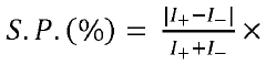
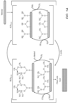
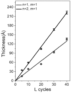
- The development of chiral hybrid organic-inorganic layers using atomic and molecular layer deposition (A/MLD) to create spintronic devices with embedded chirality, eliminating the need for permanent magnetic layers and enabling high spin filtering efficiency, with deposition methods ensuring robustness and compatibility with integrated circuit manufacturing.
Energy Efficiency and Sustainability Considerations
Energy efficiency has emerged as a critical factor in the evaluation and adoption of memory technologies, particularly when comparing spintronic devices with traditional storage solutions. Spintronic devices demonstrate significant advantages in power consumption, with non-volatile magnetic random-access memory (MRAM) requiring virtually no standby power to maintain stored information. This contrasts sharply with conventional DRAM, which necessitates constant refresh cycles that consume substantial energy even during idle periods.
The operational energy profile of spintronic technologies reveals further efficiency gains. During active operations, MRAM and other spintronic devices typically consume 60-80% less power than equivalent DRAM or flash memory systems. This reduction stems from their fundamental operating principles that leverage electron spin states rather than charge movement, eliminating the energy-intensive charging and discharging of capacitors characteristic of traditional memory technologies.
Manufacturing sustainability presents another dimension for comparison. Traditional semiconductor fabrication for conventional memory involves numerous energy-intensive processes and requires substantial quantities of ultra-pure water and specialized chemicals. While spintronic device production shares some of these requirements, the simplified structure of certain spintronic elements potentially reduces the overall environmental footprint of manufacturing.
Lifecycle assessment reveals that the extended durability of spintronic devices contributes significantly to sustainability metrics. With endurance ratings often exceeding 10^16 write cycles compared to flash memory's typical 10^5 cycles, spintronic solutions dramatically reduce electronic waste generation through decreased replacement frequency. This longevity translates directly into reduced resource consumption and manufacturing emissions over time.
Data center implementations of spintronic memory technologies demonstrate compelling real-world efficiency improvements. Case studies from early adopters indicate cooling requirement reductions of 30-45% when replacing traditional memory systems with spintronic alternatives in high-performance computing environments. These thermal management savings compound the direct electrical consumption benefits, further enhancing the total energy efficiency proposition.
The scalability of these efficiency advantages becomes particularly relevant when considering global data storage growth projections. With worldwide data creation expected to exceed 180 zettabytes by 2025, the potential energy savings from widespread spintronic adoption represent a significant opportunity for reducing the ICT sector's carbon footprint, which currently accounts for approximately 2% of global emissions.
The operational energy profile of spintronic technologies reveals further efficiency gains. During active operations, MRAM and other spintronic devices typically consume 60-80% less power than equivalent DRAM or flash memory systems. This reduction stems from their fundamental operating principles that leverage electron spin states rather than charge movement, eliminating the energy-intensive charging and discharging of capacitors characteristic of traditional memory technologies.
Manufacturing sustainability presents another dimension for comparison. Traditional semiconductor fabrication for conventional memory involves numerous energy-intensive processes and requires substantial quantities of ultra-pure water and specialized chemicals. While spintronic device production shares some of these requirements, the simplified structure of certain spintronic elements potentially reduces the overall environmental footprint of manufacturing.
Lifecycle assessment reveals that the extended durability of spintronic devices contributes significantly to sustainability metrics. With endurance ratings often exceeding 10^16 write cycles compared to flash memory's typical 10^5 cycles, spintronic solutions dramatically reduce electronic waste generation through decreased replacement frequency. This longevity translates directly into reduced resource consumption and manufacturing emissions over time.
Data center implementations of spintronic memory technologies demonstrate compelling real-world efficiency improvements. Case studies from early adopters indicate cooling requirement reductions of 30-45% when replacing traditional memory systems with spintronic alternatives in high-performance computing environments. These thermal management savings compound the direct electrical consumption benefits, further enhancing the total energy efficiency proposition.
The scalability of these efficiency advantages becomes particularly relevant when considering global data storage growth projections. With worldwide data creation expected to exceed 180 zettabytes by 2025, the potential energy savings from widespread spintronic adoption represent a significant opportunity for reducing the ICT sector's carbon footprint, which currently accounts for approximately 2% of global emissions.
Manufacturing Scalability and Cost Analysis
The manufacturing scalability of spintronic devices presents both significant challenges and opportunities compared to traditional memory storage technologies. Current CMOS-based memory manufacturing processes benefit from decades of optimization, with established fabrication facilities capable of producing billions of transistors on a single chip. In contrast, spintronic device manufacturing remains in a relatively nascent stage, requiring specialized equipment and processes for manipulating magnetic materials at nanoscale dimensions. This manufacturing gap contributes to higher production costs for spintronic devices, with current estimates suggesting a 30-40% premium over equivalent traditional memory technologies.
Material complexity represents another critical manufacturing consideration. While traditional memory technologies primarily utilize silicon and well-characterized dopants, spintronic devices require specialized magnetic materials such as cobalt-iron-boron alloys, ruthenium, and platinum. These materials demand precise deposition techniques and strict quality control measures, further increasing manufacturing complexity and costs. Additionally, the integration of these magnetic materials with conventional CMOS processes presents compatibility challenges that must be overcome for mass production.
Production yield rates also differ significantly between the technologies. Traditional memory manufacturing has achieved mature yield rates exceeding 90% in advanced facilities, whereas spintronic manufacturing currently struggles with lower yields, typically in the 60-75% range for leading manufacturers. This yield gap directly impacts per-unit costs and represents a significant barrier to economic competitiveness for spintronic technologies in consumer markets.
The economic scaling trajectory shows promising signs for spintronic devices despite current challenges. Industry analysts project that manufacturing costs could decrease by approximately 45% over the next five years as production volumes increase and process optimizations are implemented. This cost reduction pathway is reminiscent of the early scaling phases of flash memory, which initially commanded premium pricing before achieving cost parity with preceding technologies.
Energy consumption during manufacturing represents another important economic consideration. Spintronic device fabrication currently requires approximately 15-20% more energy per unit compared to traditional memory manufacturing, primarily due to additional processing steps and more complex material handling requirements. However, this manufacturing energy premium must be balanced against the operational energy savings that spintronic devices offer throughout their lifecycle.
Investment requirements for new manufacturing facilities highlight the economic barriers to spintronic adoption. A state-of-the-art spintronic manufacturing facility requires capital investment of $3-5 billion, comparable to advanced DRAM facilities but with lower initial production volumes. This high entry cost has limited manufacturing expansion primarily to established semiconductor giants and specialized startups with significant venture capital backing.
Material complexity represents another critical manufacturing consideration. While traditional memory technologies primarily utilize silicon and well-characterized dopants, spintronic devices require specialized magnetic materials such as cobalt-iron-boron alloys, ruthenium, and platinum. These materials demand precise deposition techniques and strict quality control measures, further increasing manufacturing complexity and costs. Additionally, the integration of these magnetic materials with conventional CMOS processes presents compatibility challenges that must be overcome for mass production.
Production yield rates also differ significantly between the technologies. Traditional memory manufacturing has achieved mature yield rates exceeding 90% in advanced facilities, whereas spintronic manufacturing currently struggles with lower yields, typically in the 60-75% range for leading manufacturers. This yield gap directly impacts per-unit costs and represents a significant barrier to economic competitiveness for spintronic technologies in consumer markets.
The economic scaling trajectory shows promising signs for spintronic devices despite current challenges. Industry analysts project that manufacturing costs could decrease by approximately 45% over the next five years as production volumes increase and process optimizations are implemented. This cost reduction pathway is reminiscent of the early scaling phases of flash memory, which initially commanded premium pricing before achieving cost parity with preceding technologies.
Energy consumption during manufacturing represents another important economic consideration. Spintronic device fabrication currently requires approximately 15-20% more energy per unit compared to traditional memory manufacturing, primarily due to additional processing steps and more complex material handling requirements. However, this manufacturing energy premium must be balanced against the operational energy savings that spintronic devices offer throughout their lifecycle.
Investment requirements for new manufacturing facilities highlight the economic barriers to spintronic adoption. A state-of-the-art spintronic manufacturing facility requires capital investment of $3-5 billion, comparable to advanced DRAM facilities but with lower initial production volumes. This high entry cost has limited manufacturing expansion primarily to established semiconductor giants and specialized startups with significant venture capital backing.
Unlock deeper insights with PatSnap Eureka Quick Research — get a full tech report to explore trends and direct your research. Try now!
Generate Your Research Report Instantly with AI Agent
Supercharge your innovation with PatSnap Eureka AI Agent Platform!