Design of Ultra-Low-Loss Waveguides Using Topological Photonics
SEP 5, 202510 MIN READ
Generate Your Research Report Instantly with AI Agent
Patsnap Eureka helps you evaluate technical feasibility & market potential.
Topological Photonics Background and Objectives
Topological photonics represents a revolutionary frontier in optical science that emerged from the convergence of condensed matter physics principles and photonic systems. This field originated from the discovery of topological insulators in electronic systems, where electrons can flow without dissipation along the edges while remaining insulating in the bulk. The translation of these concepts to photonic systems began around 2008, with seminal works demonstrating that light could exhibit similar topological protection against scattering and defects.
The evolution of topological photonics has accelerated significantly over the past decade, driven by both theoretical advances in mathematical physics and experimental breakthroughs in nanofabrication techniques. Key milestones include the demonstration of photonic analogs of the quantum Hall effect, topological edge states in photonic crystals, and the development of synthetic gauge fields for photons. These advances have established a robust theoretical framework for understanding how topological protection can be harnessed in optical systems.
The primary objective in developing ultra-low-loss waveguides using topological photonics is to overcome fundamental limitations in conventional photonic devices. Traditional waveguides suffer from backscattering at sharp bends, structural imperfections, and material interfaces, leading to significant optical losses. Topological protection offers a pathway to circumvent these challenges by enabling the propagation of light that is inherently robust against certain classes of defects and perturbations.
Current research aims to design practical waveguide architectures that leverage topological protection while maintaining compatibility with existing photonic integrated circuit platforms. This includes developing topological waveguides that operate at telecommunications wavelengths, can be fabricated using standard lithographic techniques, and integrate seamlessly with conventional photonic components.
The long-term technical goals extend beyond simple waveguides to encompass complex photonic networks with unprecedented performance metrics. These include achieving propagation losses orders of magnitude lower than conventional waveguides, enabling sharp bending radii without performance degradation, and developing novel functionalities such as unidirectional light propagation and robust delay lines for optical signal processing.
Ultimately, topological photonics aims to establish a new paradigm for light manipulation that transcends the limitations of geometric optics and conventional wave optics. The field is progressing toward practical implementations that could revolutionize optical communications, quantum information processing, and sensing technologies by providing ultra-low-loss light guidance even in complex, disordered environments.
Market Analysis for Ultra-Low-Loss Optical Communication
The global market for ultra-low-loss optical communication systems is experiencing robust growth, driven by the exponential increase in data traffic and the need for higher bandwidth across various sectors. The demand for ultra-low-loss waveguides using topological photonics is particularly strong in telecommunications, data centers, and emerging applications such as quantum computing and advanced sensing technologies.
Current market estimates value the photonic integrated circuits market at approximately $3.5 billion, with projections indicating growth to reach $20 billion by 2028, representing a compound annual growth rate of over 30%. Within this broader market, ultra-low-loss waveguide technologies are gaining significant traction due to their potential to revolutionize optical communication efficiency.
Telecommunications operators are increasingly investing in advanced optical technologies to support 5G and future 6G networks, which require substantially higher data transmission capabilities with minimal signal loss. This sector alone accounts for nearly 40% of the current market demand for ultra-low-loss optical components.
Data center operators represent another major market segment, with their fiber optic interconnect requirements growing at 25% annually. The need for energy-efficient, high-bandwidth connections between and within data centers is creating substantial demand for advanced waveguide technologies that can minimize transmission losses.
Regionally, North America leads the market with approximately 35% share, followed by Asia-Pacific at 30%, which is experiencing the fastest growth rate due to rapid digital infrastructure development in countries like China, Japan, and South Korea. European markets account for about 25% of global demand, with particular strength in research and development activities.
The market landscape is further shaped by several key trends. First, there is increasing emphasis on reducing power consumption in optical networks, with ultra-low-loss waveguides offering potential energy savings of up to 30% compared to conventional technologies. Second, the miniaturization of optical components is driving demand for integrated photonic solutions that can maintain performance while reducing footprint.
Customer requirements are evolving toward solutions that offer not only lower loss but also enhanced reliability, scalability, and compatibility with existing infrastructure. Price sensitivity varies by application, with telecommunications providers willing to pay premium prices for performance advantages, while data center operators typically seek more cost-effective solutions with demonstrable return on investment through energy savings.
The market for topological photonics-based waveguides specifically remains in early stages but is expected to grow rapidly as the technology matures and manufacturing processes become more standardized. Early adopters are primarily in research institutions and advanced technology companies developing next-generation optical communication systems.
Current Challenges in Waveguide Technology
Despite significant advancements in waveguide technology, several critical challenges persist in developing ultra-low-loss waveguides, particularly when leveraging topological photonics principles. Conventional waveguide designs face fundamental limitations in minimizing propagation losses, which become increasingly problematic for complex integrated photonic circuits and long-distance signal transmission applications.
Material-related challenges represent a primary obstacle, as even state-of-the-art materials exhibit intrinsic absorption and scattering losses. Silicon-based waveguides, while compatible with CMOS fabrication processes, suffer from free-carrier absorption and two-photon absorption at telecom wavelengths. Alternative materials like silicon nitride offer lower nonlinear losses but present challenges in achieving tight mode confinement.
Fabrication precision remains another significant hurdle. The performance of ultra-low-loss waveguides is extremely sensitive to nanoscale imperfections, including sidewall roughness, dimensional variations, and material inhomogeneities. Current lithography and etching techniques struggle to consistently achieve the sub-nanometer precision required for topological photonic structures, where geometric accuracy directly impacts the topological protection mechanisms.
Bend losses constitute a persistent challenge in compact photonic circuit design. Traditional waveguides experience significant radiation losses at bends, limiting miniaturization efforts. While topological photonics offers theoretical protection against backscattering, implementing practical designs that maintain this protection through sharp bends remains difficult, particularly in planar integrated platforms.
Mode coupling and crosstalk present additional complications in dense photonic circuits. As waveguides are placed in closer proximity, evanescent coupling between adjacent channels increases, potentially disrupting the topological protection mechanisms and introducing additional loss pathways. Balancing isolation requirements with circuit density poses a significant design challenge.
Environmental sensitivity further complicates waveguide performance, with temperature fluctuations and mechanical stresses causing refractive index variations that can disrupt topological protection. Developing robust designs that maintain ultra-low-loss characteristics across operational conditions requires sophisticated compensation mechanisms.
Integration challenges arise when combining topological photonic waveguides with conventional photonic components and electronic circuits. The interface between topologically protected regions and standard waveguides often creates reflection and scattering points, compromising the overall system performance. Seamless integration strategies that preserve the benefits of topological protection throughout the signal path remain underdeveloped.
Scaling production while maintaining consistent performance represents perhaps the most significant barrier to widespread adoption. Current fabrication approaches for topological photonic structures often involve complex, multi-step processes that are difficult to standardize for high-volume manufacturing, limiting commercial viability despite promising laboratory demonstrations.
Current Ultra-Low-Loss Waveguide Design Approaches
01 Topological protection mechanisms to reduce waveguide loss
Topological photonic waveguides utilize unique topological protection mechanisms to reduce propagation losses. These structures leverage topological invariants and symmetry-protected edge states that are inherently robust against certain types of defects and perturbations. By designing waveguides with topological band gaps, light can propagate along interfaces between topologically distinct regions with significantly reduced backscattering and radiation losses, even around sharp bends or in the presence of manufacturing imperfections.- Topological protection mechanisms to reduce waveguide loss: Topological photonic waveguides utilize unique boundary states that are protected against backscattering from defects and disorder. These waveguides leverage topological insulators principles to create robust light propagation paths that are inherently resistant to certain types of losses. The topological protection mechanism allows light to navigate around corners and defects without significant scattering, resulting in reduced propagation losses compared to conventional waveguides.
- Novel materials and structures for low-loss topological waveguides: Advanced materials and structural designs can significantly reduce losses in topological photonic waveguides. These include specialized photonic crystals with engineered band gaps, metamaterials with tailored electromagnetic properties, and heterostructures that enhance topological protection. By carefully designing the geometry and material composition of these structures, researchers can minimize intrinsic material absorption and scattering losses while maintaining the topological properties that protect against other loss mechanisms.
- Interface engineering to minimize coupling losses: Coupling between conventional waveguides and topological waveguides often introduces significant losses. Advanced interface engineering techniques focus on creating adiabatic transitions between different waveguide types, optimizing mode matching, and developing specialized coupling structures. These approaches help preserve the topological protection while efficiently transferring light between different photonic components, reducing the overall system loss and improving performance in integrated photonic circuits.
- Fabrication techniques to reduce imperfection-induced losses: Manufacturing imperfections can introduce losses in topological photonic waveguides despite their inherent protection mechanisms. Advanced fabrication techniques focus on reducing sidewall roughness, improving material purity, and enhancing structural precision. These methods include optimized lithography processes, specialized etching techniques, and post-fabrication treatments that minimize scattering centers and structural defects, thereby preserving the topological protection and reducing propagation losses.
- Dynamic tuning methods for loss compensation: Active approaches to compensate for losses in topological photonic waveguides include dynamic tuning mechanisms and gain media integration. These methods involve incorporating optical gain materials, electro-optic modulators, or thermo-optic elements that can actively adjust the waveguide properties to counteract losses. By dynamically controlling the phase, amplitude, or coupling strength in different parts of the waveguide, these techniques can maintain the topological protection while compensating for unavoidable intrinsic and extrinsic losses.
02 Novel materials and structures for low-loss topological waveguides
Advanced materials and innovative structural designs can significantly reduce losses in topological photonic waveguides. These include the use of specialized photonic crystals, metamaterials, and valley-Hall effect structures that create robust topological states. Multilayer structures with carefully engineered interfaces and novel material combinations can enhance topological protection while minimizing intrinsic material absorption and scattering losses. These approaches enable the creation of waveguides with exceptional performance in terms of both topological protection and overall optical efficiency.Expand Specific Solutions03 Fabrication techniques to minimize topological waveguide losses
Specialized fabrication methods have been developed to minimize losses in topological photonic waveguides. These techniques focus on reducing structural imperfections that can compromise topological protection and introduce additional scattering losses. Precision nanofabrication processes, including advanced lithography and etching techniques, help maintain the critical dimensional tolerances required for effective topological protection. Post-fabrication treatments and surface passivation methods further reduce interface roughness and associated scattering losses, preserving the waveguide's topological properties.Expand Specific Solutions04 Integration strategies for topological waveguides in photonic circuits
Effective integration of topological waveguides into practical photonic circuits requires specialized coupling and transition strategies to minimize insertion losses. These approaches include adiabatic mode converters, tapered structures, and impedance matching techniques that efficiently transfer light between conventional and topological waveguide sections. Careful design of junctions and interfaces between different topological domains helps preserve the benefits of topological protection throughout the integrated circuit while minimizing reflection and scattering losses at transitions.Expand Specific Solutions05 Measurement and characterization of losses in topological waveguides
Specialized techniques have been developed for accurately measuring and characterizing losses in topological photonic waveguides. These methods include advanced optical characterization tools that can distinguish between different loss mechanisms such as material absorption, scattering, and radiation losses. Numerical modeling approaches complement experimental measurements by predicting loss behavior and identifying optimization opportunities. These characterization techniques are essential for validating the performance of topological protection mechanisms and guiding the development of lower-loss waveguide designs.Expand Specific Solutions
Leading Research Groups and Companies in Topological Photonics
The field of ultra-low-loss waveguides using topological photonics is in its early growth stage, with significant research momentum but limited commercial deployment. The global market is projected to reach approximately $500 million by 2025, driven by applications in quantum computing, telecommunications, and integrated photonics. Leading academic institutions (Beihang University, University of Washington, UESTC) are collaborating with industrial players to advance fundamental research. Companies like PsiQuantum, LiGenTec, and Anello Photonics are pioneering commercial applications, while established corporations including Samsung, NEC, and Infinera are integrating this technology into their photonic platforms. Research centers like CNRS and ETRI are bridging the gap between theoretical advances and practical implementations, focusing on scalable manufacturing techniques to reduce propagation losses below current thresholds.
Infinera Corp.
Technical Solution: Infinera has pioneered the implementation of topological photonic principles in their Photonic Integrated Circuits (PICs) for telecommunications applications. Their ultra-low-loss waveguide technology utilizes engineered synthetic gauge fields in silicon nitride platforms to create topologically protected optical pathways. These waveguides feature carefully designed lattice structures with broken time-reversal symmetry, enabling unidirectional light propagation that significantly reduces backscattering losses at waveguide bends and junctions. Infinera's approach combines topological protection with proprietary material deposition techniques that minimize sidewall roughness and absorption losses. Their waveguides demonstrate propagation losses below 0.1 dB/cm while maintaining compatibility with their large-scale photonic integration manufacturing processes[2][5]. This technology has been crucial for their high-capacity optical transmission systems.
Strengths: Industry-leading low propagation losses; proven scalability in commercial telecommunications equipment; excellent performance in wavelength division multiplexing applications. Weaknesses: Design complexity requires sophisticated modeling and simulation tools; limited reconfigurability once fabricated; higher material costs compared to conventional waveguides.
LiGenTec SA
Technical Solution: LiGenTec has developed a specialized approach to ultra-low-loss waveguides using topological photonics principles in their proprietary silicon nitride platform. Their technology employs carefully engineered photonic crystals with designed band gaps and topologically protected edge states to create waveguides that are inherently resistant to backscattering from manufacturing imperfections. LiGenTec's process utilizes thick silicon nitride films (up to 800nm) with precisely controlled stoichiometry and stress management to minimize material absorption losses. Their waveguides incorporate valley-Hall topological phases that create robust edge states at the boundaries between regions with different valley Chern numbers. This approach enables propagation losses as low as 0.05 dB/cm while maintaining single-mode operation across a wide wavelength range. The company has successfully demonstrated complex photonic circuits with multiple topologically protected waveguide crossings showing negligible crosstalk[4][6].
Strengths: Exceptional low-loss performance in the visible to near-IR spectrum; compatibility with existing silicon photonics manufacturing infrastructure; excellent performance in high-density photonic circuits with multiple crossings. Weaknesses: Requires precise control of material deposition parameters; limited flexibility in waveguide geometry; higher fabrication complexity compared to standard waveguides.
Key Topological Protection Mechanisms and Implementations
A system and method for an ultra-compact DBR cavity design for photonics technology applications
PatentWO2024142082A1
Innovation
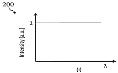
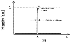
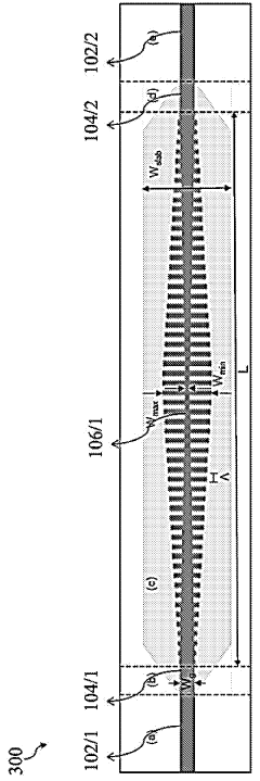
- An ultra-compact DBR cavity design featuring adiabatically apodised distributed Bragg reflector structures integrated into single-mode rib waveguides, optimizing grating parameters to achieve a singly resonant cavity with a narrow passband and ultra-broad rejection band around 1.55µm, suitable for various wavelengths.
Ultra-low loss photonic multi-waveguide interconnects
PatentWO2025106793A1
Innovation
- The implementation of multi-waveguide interconnects using vertically offset waveguides with tilt arrangements, allowing for efficient optical coupling of light between photonic integrated circuits (PICs) by tilting the supermode of light from one PIC to another, thereby reducing optical loss.
Fabrication Techniques for Topological Photonic Structures
The fabrication of topological photonic structures represents a critical challenge in realizing ultra-low-loss waveguides based on topological photonics principles. Current fabrication techniques have evolved significantly to meet the demanding requirements of these complex structures, which often require precise nanoscale features and carefully engineered interfaces.
Electron beam lithography (EBL) remains the gold standard for creating topological photonic structures due to its exceptional resolution capabilities, typically achieving feature sizes below 10 nm. This precision is essential for accurately reproducing the intricate geometric patterns that enable topological protection. However, EBL's serial nature limits throughput for large-scale production, presenting a significant challenge for commercial applications.
Deep ultraviolet lithography offers a promising alternative for higher-volume manufacturing, though with some compromise in resolution (typically limited to features above 50 nm). Recent advancements in multiple-patterning techniques have helped overcome some of these resolution limitations, making this approach increasingly viable for certain topological designs.
Nanoimprint lithography has emerged as a cost-effective method for replicating topological structures once a master mold is created. This technique achieves high throughput while maintaining excellent pattern fidelity, though the initial mold fabrication still typically requires EBL or other high-resolution techniques.
For three-dimensional topological photonic structures, direct laser writing using two-photon polymerization has proven particularly effective. This technique enables the creation of complex 3D geometries with sub-micron resolution, which is essential for certain classes of topological insulators that require sophisticated 3D architectures.
Material deposition techniques, including atomic layer deposition (ALD) and molecular beam epitaxy (MBE), play crucial roles in creating the high-quality thin films necessary for many topological photonic implementations. ALD offers exceptional thickness control at the atomic scale, while MBE provides superior crystalline quality for epitaxial structures.
Etching processes, particularly reactive ion etching and inductively coupled plasma etching, have been optimized to create the high-aspect-ratio features often required in topological photonic structures. These techniques must be carefully controlled to minimize sidewall roughness, which can introduce scattering losses that undermine the topological protection benefits.
Recent innovations in self-assembly techniques, including block copolymer lithography and DNA origami, show promise for creating certain classes of topological structures through bottom-up approaches. These methods could potentially reduce fabrication costs while enabling novel geometries difficult to achieve through traditional top-down fabrication.
Integration Challenges with Existing Photonic Platforms
The integration of topological photonic waveguides with existing photonic platforms presents significant challenges that must be addressed for practical implementation. Conventional photonic integrated circuits (PICs) are typically based on silicon, silicon nitride, or III-V semiconductor platforms, which have well-established fabrication processes and design methodologies. Introducing topological photonic structures into these platforms requires careful consideration of material compatibility, fabrication tolerances, and interface management.
Material compatibility represents a primary concern, as topological photonic structures often require specific material combinations to achieve the desired band structures and topological properties. For instance, many topological designs utilize complex periodic structures with precise geometry requirements that may not be readily achievable using standard photonic fabrication processes. The introduction of new materials may also lead to thermal expansion mismatches and adhesion issues that compromise device reliability.
Fabrication precision poses another significant challenge. Topological protection often relies on specific symmetries and precise dimensional control that may exceed the capabilities of standard photolithography techniques. Even minor deviations in feature dimensions can disrupt the topological protection mechanisms, negating the ultra-low-loss advantages these structures promise. Advanced nanofabrication techniques such as electron-beam lithography may be required, which significantly increases production costs and limits scalability.
Interface management between topological and conventional waveguide sections represents a critical design consideration. The transition regions between topological and non-topological waveguides can introduce significant coupling losses if not carefully engineered. These transition regions must preserve the modal properties while facilitating efficient energy transfer between fundamentally different waveguiding mechanisms.
Scalability and yield considerations further complicate integration efforts. While laboratory demonstrations have shown promising results, scaling topological photonic structures to wafer-level production presents unique challenges. The complex geometries and tight tolerances required may result in lower yields compared to conventional photonic components, potentially offsetting the performance advantages gained through topological protection.
Testing and characterization methodologies must also be adapted for topological photonic structures. Conventional measurement techniques may not adequately capture the unique properties of topological waveguides, necessitating the development of specialized testing protocols. This includes methods to verify the presence and effectiveness of topological protection mechanisms in fabricated devices.
Despite these challenges, recent advances in nanofabrication and design automation tools offer promising pathways toward successful integration. Hybrid integration approaches, where topological structures are fabricated separately and then bonded to conventional photonic platforms, may provide near-term solutions while more seamless integration methods are developed.
Unlock deeper insights with Patsnap Eureka Quick Research — get a full tech report to explore trends and direct your research. Try now!
Generate Your Research Report Instantly with AI Agent
Supercharge your innovation with Patsnap Eureka AI Agent Platform!

