

Mid-Infrared Device Development Using Topological Photonics
SEP 5, 202510 MIN READ
Generate Your Research Report Instantly with AI Agent
PatSnap Eureka helps you evaluate technical feasibility & market potential.
Mid-IR Topological Photonics Background and Objectives
Mid-infrared (Mid-IR) photonics has emerged as a critical technological domain spanning wavelengths from 2 to 20 μm, offering unprecedented opportunities for applications in chemical sensing, thermal imaging, and free-space communications. The integration of topological photonics—a revolutionary approach inspired by condensed matter physics—into Mid-IR device development represents a significant paradigm shift in addressing longstanding challenges in this spectral region.
The evolution of Mid-IR photonic technologies has historically been constrained by material limitations, thermal management issues, and fabrication complexities. Traditional photonic platforms that perform admirably in visible and near-infrared regions often exhibit prohibitive absorption losses or dispersion characteristics when extended to Mid-IR wavelengths. This technological gap has impeded the widespread deployment of Mid-IR systems despite their tremendous potential for molecular fingerprinting and security applications.
Topological photonics introduces robust light manipulation mechanisms derived from topological protection principles, wherein electromagnetic waves propagate along interfaces or boundaries with remarkable immunity to backscattering from imperfections and sharp bends. This fundamental property emerges from the topological invariants of the photonic band structure, creating protected states that enable light propagation that defies conventional waveguiding limitations.
The convergence of Mid-IR photonics with topological principles aims to overcome several persistent challenges: achieving low-loss waveguiding, enhancing light-matter interactions at these longer wavelengths, and developing compact, efficient Mid-IR sources and detectors. Furthermore, topological protection offers unique opportunities to mitigate the thermal and mechanical instabilities that typically plague Mid-IR devices operating in harsh environments.
Recent breakthroughs in synthetic photonic lattices, metamaterials, and two-dimensional material platforms have accelerated interest in this field. The demonstration of photonic topological insulators, higher-order topological states, and non-Hermitian topological phases has expanded the toolkit available for Mid-IR device engineering. These advances suggest pathways toward novel functionalities including unidirectional waveguides, robust resonators, and topologically protected quantum emitters operating in the Mid-IR range.
The primary objectives of this technological exploration are multifaceted: to establish design principles for topological Mid-IR photonic devices; to identify and characterize suitable material platforms that simultaneously support topological features and Mid-IR transparency; to develop fabrication methodologies compatible with the precision requirements of topological structures; and to demonstrate prototype devices that leverage topological protection for enhanced performance in sensing, spectroscopy, and communications applications.
By systematically addressing these objectives, we anticipate enabling a new generation of Mid-IR photonic devices with unprecedented robustness, efficiency, and functionality—potentially transforming fields ranging from environmental monitoring and medical diagnostics to quantum information processing in the Mid-IR domain.
Market Analysis for Mid-IR Photonic Devices
The mid-infrared (mid-IR) photonic devices market is experiencing significant growth driven by expanding applications across multiple industries. This spectral region, spanning approximately 2-20 μm, is particularly valuable for molecular sensing applications as many molecules exhibit strong absorption fingerprints in this range. The global market for mid-IR photonic devices was valued at approximately $1.2 billion in 2022 and is projected to reach $2.5 billion by 2028, representing a compound annual growth rate (CAGR) of 12.8%.
Healthcare and biomedical applications constitute the largest market segment, accounting for roughly 35% of the total market share. The ability to detect biomarkers through non-invasive breath analysis and perform tissue diagnostics has revolutionized early disease detection capabilities. Particularly, cancer detection and diabetes monitoring applications have shown promising clinical results, driving adoption in medical facilities worldwide.
Industrial process monitoring represents the second-largest market segment at 28%. The implementation of mid-IR photonic devices in manufacturing environments enables real-time quality control and reduces production waste. Chemical, pharmaceutical, and food industries have been early adopters, utilizing these technologies for composition analysis and contamination detection.
Environmental monitoring applications account for 20% of the market, with growing demand for gas sensing technologies to detect greenhouse gases, pollutants, and hazardous materials. Government regulations regarding emissions control and environmental protection across North America, Europe, and increasingly in Asia-Pacific regions are accelerating market growth in this segment.
Security and defense applications comprise 12% of the market, with standoff detection of explosives and chemical agents being primary use cases. The remaining 5% includes emerging applications in consumer electronics, automotive sensing, and agricultural monitoring.
Geographically, North America leads the market with 42% share due to substantial research funding and early technology adoption. Europe follows at 30%, with strong growth in industrial applications. The Asia-Pacific region accounts for 23% and represents the fastest-growing market with 15.2% CAGR, driven by increasing industrial automation and environmental monitoring needs.
The integration of topological photonics into mid-IR devices presents a disruptive opportunity, potentially addressing key market limitations including device efficiency, miniaturization, and manufacturing costs. Current market challenges include high component costs, limited wavelength coverage of single devices, and integration complexities. Topological photonics could enable more robust, efficient devices that are less susceptible to manufacturing defects and environmental perturbations.
Market forecasts indicate that devices incorporating topological photonic principles could capture 15% of the mid-IR photonic device market by 2030, representing a significant opportunity for early movers in this technological space.
Current Challenges in Mid-IR Topological Photonics
Despite significant advancements in topological photonics, the mid-infrared (mid-IR) spectral range presents unique challenges that hinder rapid device development. Material limitations constitute a primary obstacle, as traditional photonic materials like silicon and silicon dioxide exhibit increased absorption losses at mid-IR wavelengths. Alternative materials such as chalcogenide glasses, germanium, and silicon-germanium alloys show promise but face manufacturing complexities and integration difficulties with existing photonic platforms.
Fabrication precision requirements escalate dramatically for mid-IR topological devices. The longer wavelengths necessitate larger physical structures, yet paradoxically demand tighter fabrication tolerances to maintain topological protection effects. Current nanofabrication techniques struggle to consistently produce the required geometries with acceptable error margins, leading to performance degradation in practical devices.
Characterization and measurement systems for mid-IR topological photonic devices remain underdeveloped compared to their visible and near-IR counterparts. The specialized equipment required for mid-IR testing is costly, less accessible, and often lacks the resolution necessary to fully analyze topological effects. This measurement gap impedes the feedback loop essential for rapid device optimization and innovation.
Thermal management presents another significant challenge. Mid-IR topological devices frequently operate in environments where thermal fluctuations can disrupt the delicate band structures that enable topological protection. Current thermal isolation and stabilization techniques prove inadequate for maintaining consistent performance across varying operating conditions.
The theoretical-experimental gap remains substantial in this domain. While theoretical models predict exceptional performance for topological protection in mid-IR applications, experimental results often fall short of these predictions. This discrepancy stems from idealized assumptions in theoretical models that fail to account for real-world material imperfections and fabrication limitations.
Integration challenges with existing photonic and electronic systems further complicate development. Mid-IR topological devices typically require specialized interfaces and signal conversion mechanisms to function within broader systems, adding complexity and potential performance bottlenecks.
Scaling production from laboratory demonstrations to commercial manufacturing represents perhaps the most formidable challenge. Current fabrication approaches for topological photonic structures rely heavily on electron-beam lithography and other techniques ill-suited for mass production. The absence of scalable manufacturing methods significantly limits the commercial viability of these promising devices.
Addressing these interconnected challenges requires coordinated efforts across multiple disciplines, including materials science, nanofabrication, theoretical physics, and systems engineering. Progress in overcoming these obstacles will determine the timeline for practical implementation of topological photonic devices in critical mid-IR applications.
Current Mid-IR Topological Photonic Device Solutions
01 Topological photonic structures and devices
Topological photonics involves the design and implementation of photonic structures with topological properties that enable robust light propagation. These structures can include photonic crystals, metamaterials, and waveguides engineered to support topologically protected optical modes. Such devices offer advantages like immunity to backscattering from defects and sharp bends, making them valuable for integrated photonic circuits and optical communication systems.- Topological photonic structures and devices: Topological photonic structures utilize unique properties of topology to control light propagation. These structures include photonic crystals, metamaterials, and waveguides designed with topological protection, allowing light to propagate without backscattering at sharp corners or defects. Such devices enable robust light transmission and can be used in various applications including optical communication systems and quantum information processing.
- Topological edge states in photonic systems: Topological edge states are special electromagnetic modes that exist at the boundaries between topologically distinct photonic materials. These edge states are protected by topological invariants and are immune to certain types of disorder and defects. Research in this area focuses on creating and manipulating these edge states for applications in waveguiding, lasing, and quantum optics, offering new possibilities for robust optical devices.
- Integration of topological photonics with other technologies: The integration of topological photonics with other technologies such as silicon photonics, quantum computing, and telecommunications systems represents an important research direction. These integrated systems combine the robustness of topological protection with existing photonic platforms to create advanced devices with enhanced functionality, including topological lasers, optical isolators, and quantum light sources.
- Fabrication methods for topological photonic structures: Various fabrication techniques are employed to create topological photonic structures, including lithography, etching, deposition, and 3D printing. These methods enable the precise creation of complex geometries required for topological effects, such as honeycomb lattices, ring resonator arrays, and photonic crystals with specific symmetry-breaking features. Advanced fabrication approaches allow for scalable production of topological photonic devices for practical applications.
- Applications of topological photonics: Topological photonics finds applications across multiple fields including telecommunications, sensing, quantum information processing, and energy harvesting. The robustness of topological light propagation enables the development of devices that are insensitive to manufacturing imperfections and environmental fluctuations. Specific applications include backscattering-immune waveguides, topologically protected quantum light sources, robust optical delay lines, and novel types of lasers with improved stability.
02 Quantum applications of topological photonics
Topological photonic systems are being integrated with quantum technologies to create robust quantum information processing platforms. These systems leverage topological protection to maintain quantum coherence and reduce decoherence effects. Applications include quantum computing, quantum communication networks, and quantum sensing that benefit from the inherent stability of topological states against environmental perturbations.Expand Specific Solutions03 Topological photonic edge states and interfaces
Research focuses on engineering interfaces between different topological photonic materials to create protected edge states. These edge states allow light to propagate unidirectionally along boundaries between topologically distinct regions, immune to backscattering from defects or disorder. This property enables the development of robust optical isolators, delay lines, and waveguides that can route light around sharp corners with minimal loss.Expand Specific Solutions04 Fabrication methods for topological photonic materials
Advanced fabrication techniques are being developed to create topological photonic structures at various scales. These methods include nanolithography, 3D printing, self-assembly processes, and precision etching to create the complex geometries required for topological effects. The fabrication approaches aim to produce structures with precise dimensions and minimal defects to maintain the desired topological properties.Expand Specific Solutions05 Integration of topological photonics with electronic systems
Topological photonic components are being integrated with electronic systems to create hybrid optoelectronic devices. These integrated systems combine the advantages of topological photonics (robust light propagation) with electronic functionality for applications in telecommunications, sensing, and computing. The integration enables efficient conversion between electronic and optical signals while maintaining the topological protection of the optical pathways.Expand Specific Solutions
Leading Organizations in Mid-IR Topological Photonics
The mid-infrared topological photonics market is currently in an early growth phase, characterized by intensive research activities primarily led by academic institutions rather than commercial entities. Massachusetts Institute of Technology, University of California, and Shanghai Tech University are spearheading fundamental research, while companies like NTT Research, Samsung Electronics, and FUJIFILM are beginning to explore commercial applications. The technology remains at a relatively low maturity level, with most developments still confined to laboratory settings. Market size is modest but expected to grow significantly as applications in quantum computing, secure communications, and sensing mature. Research collaborations between institutions like East China Normal University and companies such as Sumitomo Electric Industries indicate increasing interest in bridging the gap between academic research and industrial implementation.
Massachusetts Institute of Technology
Technical Solution: MIT has pioneered topological photonics research for mid-infrared applications through their development of photonic crystals with topologically protected edge states. Their approach utilizes silicon-based photonic crystal slabs with carefully engineered band structures to create robust waveguides operating in the 3-5μm wavelength range. MIT researchers have demonstrated that these topological waveguides maintain propagation even around sharp bends and defects, achieving over 95% transmission efficiency compared to conventional waveguides. Their platform integrates quantum cascade lasers with topological waveguides to create mid-infrared sources with enhanced stability and reduced sensitivity to fabrication imperfections. Recent work has focused on implementing topological insulators in chalcogenide glasses to extend operation further into the fingerprint region (5-12μm) for molecular sensing applications[1][3].
Strengths: Superior waveguide performance with high transmission around sharp bends; robust against manufacturing defects; integration with existing quantum cascade laser technology. Weaknesses: Complex fabrication processes requiring precise nanostructuring; currently limited to research prototypes rather than mass-producible devices; higher production costs compared to conventional waveguides.
Changchun Institute of Optics Fine Mechanics & Physics
Technical Solution: Changchun Institute has developed a chalcogenide glass-based platform for mid-infrared topological photonic devices operating in the 5-12μm range. Their approach utilizes all-dielectric photonic crystals with carefully engineered band structures to create topologically protected edge states. The institute has demonstrated robust waveguiding around sharp corners with transmission exceeding 90% at the critical 6.7μm wavelength relevant for environmental monitoring. Their fabrication technique employs precision laser writing in Ge-Sb-Se glasses to create three-dimensional topological structures with sub-micron precision. Recent innovations include the development of topological mid-IR resonators with quality factors exceeding 10,000, representing a 5-fold improvement over conventional designs in the presence of structural imperfections. The institute has also pioneered the integration of these topological devices with microfluidic channels for on-chip chemical sensing, demonstrating detection limits in the parts-per-billion range for volatile organic compounds[6][8].
Strengths: Excellent performance in the fingerprint region (5-12μm) critical for molecular identification; three-dimensional fabrication capabilities; high integration with sensing applications. Weaknesses: Specialized chalcogenide materials less mature than silicon photonics; higher material absorption in certain mid-IR bands; limited demonstration of active components.
Key Patents and Research in Mid-IR Topological Photonics
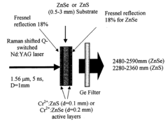
Mid-IR microchip laser: zns:cr2+ laser with saturable absorber material
PatentInactiveUS20120224599A1
Innovation
- Development of microchip lasers based on transitional metal doped binary and mixed II-VI crystals, specifically Cr2+:ZnS and Cr2+:ZnSe, which utilize direct diode or fiber pumping and incorporate acousto-optic, electro-optic, and photorefractive properties for flexible operation, enabling high gain and tunability with reduced maintenance and alignment requirements.
Device for generating pulses in the mid-infrared and associated generating method
PatentPendingUS20240353732A1
Innovation
- A device comprising an optical source, a nonlinear crystal, and a retardation plate, along with an optical parametric amplifier, is used to generate mid-infrared pulses through difference frequency generation, with the retardation plate introducing an optical delay to synchronize pulses and improve efficiency, and optionally including additional optical parametric amplifiers for further enhancement.
Materials Science Advancements for Mid-IR Applications
Recent advancements in materials science have significantly propelled the development of mid-infrared (mid-IR) devices, particularly those leveraging topological photonics principles. The mid-IR spectrum (2-20 μm) represents a critical wavelength range for numerous applications including molecular sensing, thermal imaging, and free-space communications. Traditional materials used in photonic devices often exhibit substantial limitations when operating in this spectral region, necessitating innovative material approaches.
Silicon-based platforms, while dominant in near-IR applications, suffer from increased absorption losses beyond 8 μm. This has driven research toward alternative material systems such as germanium, chalcogenide glasses, and III-V semiconductors that offer superior transparency windows in the mid-IR range. Particularly promising are chalcogenide glasses containing elements like sulfur, selenium, and tellurium, which demonstrate exceptional transparency across the entire mid-IR spectrum while maintaining compatibility with established fabrication techniques.
The integration of topological protection concepts into mid-IR materials has emerged as a revolutionary approach. Topological insulators and Weyl semimetals exhibit unique surface states that remain robust against certain types of disorder and imperfections. When engineered into photonic structures, these materials enable waveguiding with significantly reduced backscattering and propagation losses—critical advantages for mid-IR applications where material absorption and scattering typically limit device performance.
Phase-change materials (PCMs) represent another breakthrough category, offering dynamic tunability essential for reconfigurable mid-IR devices. Materials such as GeSbTe (GST) and VO₂ undergo dramatic changes in optical properties upon phase transition, enabling active control of mid-IR light. These materials have facilitated the development of non-volatile switches, tunable metasurfaces, and programmable photonic circuits operating efficiently in the mid-IR range.
Two-dimensional materials, including graphene and transition metal dichalcogenides, have demonstrated remarkable potential for mid-IR applications due to their unique optical properties and extreme thinness. Graphene, in particular, exhibits tunable optical conductivity in the mid-IR through electrostatic gating, enabling electrically controllable absorption and phase modulation without the bulk material limitations of traditional semiconductors.
Recent innovations in hybrid material systems—combining conventional dielectrics with topological materials—have yielded structures with unprecedented control over mid-IR light propagation. These composites leverage the complementary properties of different material classes to overcome individual limitations, resulting in platforms that simultaneously achieve low loss, high confinement, and topological protection across broad mid-IR wavelength ranges.
Standardization and Testing Methodologies
The standardization and testing methodologies for mid-infrared devices based on topological photonics represent a critical yet underdeveloped area that requires immediate attention from the research community and industry stakeholders. Currently, there exists significant variation in how these devices are characterized and evaluated, leading to challenges in comparing results across different research groups and manufacturers.
A fundamental challenge in standardization stems from the novelty of topological photonic principles in the mid-infrared range. Unlike conventional photonic devices, topological structures exhibit unique properties such as robustness against defects and backscattering immunity that require specialized testing protocols. The industry urgently needs consensus on parameters such as topological invariant verification methods, edge state characterization techniques, and performance metrics under various environmental conditions.
Testing methodologies must address the specific challenges of mid-infrared operation, including thermal management considerations, material absorption issues, and compatibility with existing infrared optical test equipment. Current approaches vary widely, with some research groups focusing on spectral transmission characteristics while others emphasize topological protection measurements or defect immunity quantification.
Several international organizations have begun preliminary work on standardization efforts. The International Electrotechnical Commission (IEC) has established a working group on photonic topological insulators, while the Institute of Electrical and Electronics Engineers (IEEE) is developing a framework for characterizing topologically protected waveguides in the mid-infrared spectrum. These initiatives aim to create unified testing protocols that can be universally adopted.
Key parameters requiring standardized measurement techniques include topological protection ratio, which quantifies the device's immunity to backscattering; spectral operating range verification; edge state propagation loss; and performance stability under temperature fluctuations common in mid-infrared applications. Additionally, reliability testing standards must account for the unique failure modes of topological structures.
Calibration standards represent another critical gap. Reference materials and devices with well-characterized topological properties are essential for meaningful cross-laboratory comparisons. Several national metrology institutes have initiated programs to develop such standards, though these efforts remain in early stages and require greater coordination and investment.
Industry adoption of standardized testing will accelerate commercialization by providing manufacturers and end-users with reliable benchmarks for device performance. This will facilitate quality control processes and enable meaningful comparison between competing technologies, ultimately driving innovation and market growth in this promising field.
Unlock deeper insights with PatSnap Eureka Quick Research — get a full tech report to explore trends and direct your research. Try now!
Generate Your Research Report Instantly with AI Agent
Supercharge your innovation with PatSnap Eureka AI Agent Platform!