

Two-Dimensional Material Platforms for Topological Photonics
SEP 5, 202510 MIN READ
Generate Your Research Report Instantly with AI Agent
PatSnap Eureka helps you evaluate technical feasibility & market potential.
2D Materials in Topological Photonics: Background & Objectives
Topological photonics has emerged as a revolutionary field at the intersection of condensed matter physics and optical science, offering unprecedented control over light propagation through topologically protected states. The evolution of this field traces back to the discovery of topological insulators in electronic systems, which subsequently inspired researchers to explore similar phenomena in photonic systems. Over the past decade, significant theoretical frameworks and experimental demonstrations have established topological photonics as a promising platform for robust light manipulation immune to disorder and imperfections.
Two-dimensional materials have concurrently risen as exceptional platforms for photonic applications due to their unique optical, electronic, and mechanical properties. Materials such as graphene, transition metal dichalcogenides (TMDs), hexagonal boron nitride (h-BN), and black phosphorus exhibit remarkable light-matter interactions at the atomic scale, providing unprecedented opportunities for miniaturization and integration of photonic devices.
The convergence of topological photonics with 2D materials represents a natural technological progression, leveraging the exceptional properties of both domains. This integration aims to overcome fundamental limitations in conventional photonic systems, particularly regarding robustness against fabrication imperfections, backscattering immunity, and miniaturization constraints. The field is rapidly evolving from theoretical concepts to practical implementations with potential applications in quantum information processing, optical computing, and telecommunications.
The primary technical objectives in this domain include developing scalable fabrication methods for 2D material-based topological photonic structures, achieving room-temperature operation of topological effects, and demonstrating practical devices with superior performance compared to conventional counterparts. Researchers are particularly focused on exploiting the unique properties of 2D materials, such as strong light-matter interactions, gate-tunability, and extreme confinement capabilities, to create novel topological states of light.
Recent advances in nanofabrication techniques and characterization methods have accelerated progress in this field, enabling the experimental realization of theoretical predictions. The trajectory of development suggests a transition from fundamental physics exploration to engineering applications, with increasing emphasis on device integration and performance optimization.
The ultimate goal of this technological convergence is to establish a versatile platform that combines the robustness of topological protection with the versatility and integrability of 2D materials, potentially revolutionizing next-generation photonic technologies. This would enable the development of photonic circuits immune to manufacturing defects, efficient non-reciprocal devices, and novel quantum optical interfaces operating at unprecedented scales.
Market Applications and Demand Analysis for Topological Photonic Devices
The market for topological photonic devices is experiencing significant growth driven by the unique properties of two-dimensional materials in photonic applications. Current market analysis indicates that the global photonics market is expanding at a compound annual growth rate of approximately 7%, with specialized segments like topological photonics showing even more robust growth potential due to their novel functionalities.
The primary market demand for topological photonic devices stems from telecommunications and data centers, where the need for efficient, high-bandwidth optical components continues to escalate with the exponential growth in data traffic. These sectors value the backscattering-immune waveguides and robust light propagation that topological photonics can provide, potentially revolutionizing signal transmission in optical networks.
Quantum computing represents another significant market opportunity, as topological photonic states offer inherent protection against decoherence—a critical challenge in quantum information processing. Industry analysts project that the quantum computing market will reach substantial valuation within the next decade, with photonic implementations gaining traction due to their room-temperature operation capabilities.
Sensing and metrology applications constitute a rapidly expanding market segment for topological photonic devices. The exceptional sensitivity and stability of topological edge states make them ideal for precision measurements in industrial quality control, environmental monitoring, and biomedical diagnostics. This market is particularly receptive to innovations that enhance measurement accuracy while reducing susceptibility to environmental perturbations.
Defense and aerospace industries have demonstrated increasing interest in topological photonics for secure communications and advanced sensing systems. The robustness against disorder and defects makes these technologies particularly valuable in harsh operating environments where conventional photonic systems might fail.
Consumer electronics represents a longer-term market opportunity, with potential applications in next-generation display technologies, augmented reality systems, and compact optical sensors for smart devices. While mass-market adoption faces challenges related to manufacturing scalability and cost, the unique properties of topological photonic devices could enable distinctive product features that command premium pricing.
Market research indicates that early adopters of topological photonic technologies will likely be high-performance computing, telecommunications infrastructure, and specialized scientific instrumentation sectors where performance advantages outweigh initial cost considerations. The transition to broader commercial applications will depend on advances in manufacturing techniques for two-dimensional material platforms, with industry partnerships between academic research institutions and technology companies playing a crucial role in market development.
Current Challenges in 2D Material-Based Topological Photonics
Despite significant advancements in two-dimensional material-based topological photonics, several critical challenges continue to impede the field's progress toward practical applications. One fundamental obstacle remains the fabrication of high-quality 2D materials with consistent properties at scale. Current synthesis methods often produce samples with varying defect densities and domain sizes, leading to inconsistent topological properties and compromised performance in photonic devices.
Material stability presents another significant hurdle, particularly when 2D materials interface with photonic structures. Many promising 2D materials exhibit degradation under ambient conditions or when subjected to high optical powers, limiting their practical utility in real-world applications. The challenge of encapsulation without disrupting topological properties remains largely unsolved.
The integration of 2D materials with conventional photonic platforms represents a substantial technical barrier. The atomically thin nature of these materials makes them difficult to manipulate and position precisely within photonic circuits. Current transfer techniques often introduce contaminants or create wrinkles that disrupt the material's electronic and optical properties, consequently affecting topological features.
Temperature sensitivity constitutes a significant limitation for many topological photonic systems based on 2D materials. Most demonstrations operate at cryogenic temperatures, where thermal fluctuations are minimized. Developing room-temperature topological protection mechanisms remains an outstanding challenge that requires innovative material engineering approaches.
The bandgap engineering of topological states in 2D material platforms presents complex challenges. While theoretical predictions suggest numerous possibilities, experimental realization of designed bandgaps with precise topological properties has proven difficult. The interplay between material properties, structural parameters, and topological characteristics requires sophisticated modeling and precise fabrication techniques that push the boundaries of current capabilities.
Non-linear effects in topological photonic systems based on 2D materials remain inadequately understood. While these effects could enable novel functionalities, they also introduce complexities in system behavior that are difficult to predict and control. Developing comprehensive models that accurately capture these non-linear dynamics represents a significant theoretical challenge.
Finally, characterization techniques for topological photonic states in 2D material systems need substantial improvement. Current methods often provide indirect evidence of topological properties rather than direct observation of protected edge states or their robustness against perturbations. Advanced imaging and spectroscopic techniques specifically tailored for these systems are urgently needed to accelerate progress in the field.
State-of-the-Art 2D Material Platforms for Topological Photonics
01 2D materials for topological photonic devices
Two-dimensional materials such as graphene and transition metal dichalcogenides are used as platforms for creating topological photonic devices. These materials offer unique electronic and optical properties that enable the manipulation of light at the nanoscale. By engineering the structure of these 2D materials, researchers can create photonic crystals with topological properties that allow for robust light propagation along protected edge states, which is essential for developing next-generation optical communication systems.- Two-dimensional materials for topological photonic devices: Two-dimensional materials such as graphene and transition metal dichalcogenides are used as platforms for creating topological photonic devices. These materials offer unique electronic and optical properties that enable the manipulation of light at the nanoscale. By engineering the structure of these 2D materials, researchers can create photonic crystals with topological edge states that allow for robust light propagation immune to backscattering from defects and sharp bends.
- Valley-Hall topological insulators based on 2D materials: Valley-Hall topological insulators represent a specific class of topological photonic systems that leverage the valley degree of freedom in two-dimensional materials. These systems exploit the broken inversion symmetry in honeycomb or triangular lattice structures to create topologically protected edge states. The valley-polarized edge modes enable directional light propagation that is robust against certain types of disorder, making them promising for developing optical isolators and waveguides.
- Quantum spin Hall effect in photonic systems with 2D materials: The quantum spin Hall effect can be realized in photonic systems by incorporating two-dimensional materials to create spin-orbit coupling for light. These systems feature counter-propagating edge states with opposite spin polarizations that are protected against backscattering. By integrating 2D materials like graphene or hexagonal boron nitride into photonic crystals, researchers can achieve topologically protected light transport that mimics the behavior of electronic topological insulators.
- Non-Hermitian topological photonics with 2D material platforms: Non-Hermitian topological photonics combines concepts from non-Hermitian physics (involving gain and loss) with topological protection in two-dimensional material platforms. These systems exhibit unique phenomena such as unidirectional invisibility, exceptional points, and topological phase transitions that have no counterpart in Hermitian systems. By incorporating gain and loss mechanisms in 2D material-based photonic structures, researchers can create novel devices with enhanced functionality for optical isolation and sensing applications.
- Reconfigurable topological photonic devices using 2D materials: Two-dimensional materials enable the creation of reconfigurable topological photonic devices whose properties can be dynamically tuned through external stimuli such as electrical gating, optical pumping, or mechanical strain. The high tunability of 2D materials like graphene allows for active control of topological phase transitions and edge states in real-time. These reconfigurable platforms offer advantages for developing programmable optical circuits, switches, and modulators with topological protection against fabrication imperfections.
02 Valley-Hall topological insulators based on 2D materials
Valley-Hall topological insulators represent a specific class of topological photonic systems that leverage the valley degree of freedom in 2D materials. These systems exploit the broken inversion symmetry in honeycomb or triangular lattice structures to create topologically protected edge states. The valley-polarized edge states enable unidirectional light propagation that is robust against certain types of defects and disorder, making them promising for applications in optical isolation and waveguiding.Expand Specific Solutions03 Quantum spin Hall effect in photonic systems
The quantum spin Hall effect, originally observed in electronic systems, has been successfully implemented in photonic platforms using 2D materials. These systems utilize the spin-orbit coupling of light to create helical edge states where the propagation direction is locked to the photon spin. By incorporating 2D materials into carefully designed photonic structures, researchers can achieve robust bidirectional light transport that is protected against backscattering, which is crucial for developing fault-tolerant optical circuits and quantum information processing devices.Expand Specific Solutions04 Nonlinear effects in topological photonic structures
Nonlinear optical effects in topological photonic structures based on 2D materials enable novel functionalities beyond linear light propagation. These nonlinear phenomena, including second-harmonic generation, four-wave mixing, and optical bistability, can be enhanced by the strong light-matter interactions in 2D materials. The combination of topological protection and nonlinear effects allows for the development of robust optical switches, frequency converters, and logic gates that operate with low power consumption and high efficiency.Expand Specific Solutions05 Fabrication methods for 2D material-based topological photonic structures
Various fabrication techniques have been developed to create topological photonic structures using 2D materials. These methods include lithographic patterning, self-assembly, and direct growth approaches that enable precise control over the geometric parameters necessary for achieving topological properties. Advanced nanofabrication techniques allow for the creation of complex photonic crystal structures with specific lattice geometries, defects, and interfaces that are essential for realizing topological edge states and other exotic optical phenomena in practical devices.Expand Specific Solutions
Leading Research Groups and Industry Players
The field of two-dimensional material platforms for topological photonics is currently in an early growth phase, characterized by intensive academic research transitioning toward commercial applications. The global market for topological photonics is projected to expand significantly as applications in quantum computing, telecommunications, and sensing mature. Leading academic institutions including MIT, Caltech, and Peking University are driving fundamental research, while companies like 3M Innovative Properties and Sony Group are beginning to develop practical applications. The technology remains primarily in the research domain, with academic institutions holding most intellectual property. Commercial maturity varies across applications, with quantum computing implementations still experimental while telecommunications applications are approaching practical deployment. Industry-academic partnerships between entities like Cambridge Enterprise and technology companies represent a critical pathway for technology transfer in this emerging field.
Massachusetts Institute of Technology
Technical Solution: MIT has pioneered innovative approaches in topological photonics using 2D materials, particularly focusing on valley photonic crystals based on transition metal dichalcogenides (TMDs). Their research team has developed photonic structures that leverage the valley degree of freedom in 2D materials to create robust topologically protected edge states. By engineering the interface between domains with opposite valley Chern numbers, MIT researchers have demonstrated unidirectional light propagation that is immune to backscattering from defects and sharp bends. Their platform utilizes the strong light-matter interactions in atomically thin 2D materials to achieve valley-selective circular dichroism and spin-valley coupling effects. MIT has also explored the integration of 2D materials with silicon photonics to create hybrid topological devices that can operate at room temperature with unprecedented control over light propagation.
Strengths: Superior integration with existing silicon photonics technology; exceptional control over valley-selective light propagation; demonstrated room-temperature operation. Weaknesses: Challenges in scaling up fabrication processes; potential limitations in bandwidth due to material constraints; requires precise control of 2D material quality.
University of Maryland
Technical Solution: The University of Maryland has developed innovative platforms for topological photonics using 2D materials, with a particular focus on creating higher-order topological insulators (HOTIs) using transition metal dichalcogenide (TMD) monolayers. Their approach involves engineering corner and edge states in 2D material-based photonic crystals through careful design of the lattice geometry and symmetry breaking. Maryland researchers have demonstrated robust corner states in second-order topological insulators based on WS2 and MoS2 monolayers, which exhibit strong light confinement and protection against certain types of disorder. Their platform leverages the valley-selective circular dichroism in TMDs to create valley-polarized topological corner states that can be selectively excited using circularly polarized light. This enables novel applications in valley photonics and quantum information processing. The Maryland team has also pioneered the integration of their 2D material topological photonic platforms with conventional waveguide technologies, demonstrating efficient coupling between topological corner states and waveguide modes.
Strengths: Novel higher-order topological states with robust corner localization; valley-selective excitation capabilities; demonstrated integration with conventional photonic technologies. Weaknesses: Limited operational bandwidth; sensitivity to substrate interactions affecting topological properties; challenges in precise positioning of quantum emitters within corner states.
Key Patents and Breakthrough Publications Analysis
A scalable quantum-confined device
PatentActiveUS20190288160A1
Innovation
- A quantum-confined device is fabricated using a substrate with protrusions that induce localized strain in a layer of two-dimensional material, allowing for the formation of quantum dots or quantum wires with controlled positioning and high-quality optical and electrical properties, leveraging the unique properties of two-dimensional materials like graphene and tungsten diselenide.
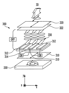
Two-dimensional and three-dimensional image selectable display device
PatentInactiveUS8174464B2
Innovation
- A display device with a barrier panel featuring liquid crystals in Electrically Controlled Birefringence (ECB) mode and In-Plane-Switching (IPS) type electrodes, allowing for user-selectable switching between two-dimensional and three-dimensional display modes, as well as wide or narrow viewing angles, by applying voltages to control the electric field and orientation of liquid crystals.
Fabrication Techniques and Manufacturing Scalability
The fabrication of two-dimensional material platforms for topological photonics represents a critical challenge in translating theoretical advances into practical applications. Current fabrication techniques primarily rely on mechanical exfoliation, chemical vapor deposition (CVD), and molecular beam epitaxy (MBE). Mechanical exfoliation, while producing high-quality samples, suffers from limited scalability and poor reproducibility, making it unsuitable for industrial applications despite its prevalence in laboratory settings.
Chemical vapor deposition has emerged as a promising approach for large-scale production of 2D materials such as graphene and transition metal dichalcogenides (TMDs). Recent advancements in CVD techniques have enabled the growth of high-quality monolayers with controlled thickness and crystallinity. However, challenges remain in achieving uniform growth over large areas and minimizing defect densities, which are crucial for maintaining topological protection in photonic systems.
Molecular beam epitaxy offers exceptional control over material composition and interface quality, essential for heterostructure-based topological photonic devices. The ultra-high vacuum conditions during MBE growth minimize contamination, resulting in atomically precise interfaces. Nevertheless, MBE processes are typically slow and expensive, limiting their application to specialized research environments rather than mass production scenarios.
The integration of 2D materials into functional topological photonic devices introduces additional manufacturing challenges. Techniques such as lithography, etching, and transfer processes must be optimized to preserve the delicate topological properties while ensuring device functionality. Particularly challenging is the precise patterning of 2D materials to create photonic crystal structures with the specific geometries required for topological band structures.
Recent innovations in nanofabrication, including advanced electron beam lithography and focused ion beam milling, have improved the precision of 2D material patterning. However, these techniques remain serial processes with limited throughput. Parallel fabrication methods, such as nanoimprint lithography and self-assembly approaches, show promise for scaling production but require further development to meet the stringent requirements of topological photonics.
The manufacturing scalability of 2D material-based topological photonic devices remains a significant bottleneck for commercial applications. Current laboratory demonstrations typically involve small-scale devices with areas of a few square millimeters. Scaling to wafer-level production necessitates addressing challenges in material uniformity, defect control, and process integration. Industry-academic collaborations are increasingly focusing on developing standardized fabrication protocols and quality control metrics to facilitate the transition from laboratory demonstrations to commercial manufacturing.
Integration Potential with Existing Photonic Technologies
The integration of two-dimensional (2D) material platforms for topological photonics with existing photonic technologies represents a critical pathway toward practical applications and commercial viability. Current silicon photonics infrastructure offers a mature foundation upon which topological photonic devices based on 2D materials can be developed. The compatibility between these platforms is particularly promising, as many 2D materials can be directly transferred onto silicon-based photonic circuits through established techniques such as mechanical exfoliation, chemical vapor deposition (CVD), or wet transfer methods.
Several integration approaches have demonstrated significant potential. The hybrid integration of graphene with silicon waveguides has enabled electro-optic modulation with unprecedented bandwidth and energy efficiency. Similarly, transition metal dichalcogenides (TMDs) have been successfully integrated with silicon nitride and silicon-on-insulator platforms to create enhanced light-matter interaction regions that preserve topological protection characteristics.
The vertical heterostructure approach, where multiple 2D materials are stacked to form functional devices, presents another integration pathway. These structures can be incorporated into conventional photonic integrated circuits (PICs) to introduce topological features while maintaining compatibility with CMOS fabrication processes. Recent demonstrations have shown that such hybrid devices can operate at telecommunications wavelengths with minimal insertion losses.
From a manufacturing perspective, wafer-scale growth and transfer techniques for 2D materials have advanced significantly, addressing previous scalability concerns. Companies like Applied Materials and AIXTRON have developed specialized equipment for large-area synthesis of 2D materials with the uniformity required for photonic applications. These developments bridge the gap between laboratory demonstrations and industrial implementation.
The temperature compatibility between 2D material processing and conventional photonic fabrication remains challenging but manageable. Most 2D material transfer and processing can be performed as back-end steps after the completion of temperature-sensitive components, enabling co-existence within the same manufacturing workflow.
Looking toward system-level integration, topological photonic devices based on 2D materials show particular promise for specialized functions within larger photonic systems. Edge states in topological photonic crystals made from 2D materials could serve as robust waveguides connecting different components in complex PICs, while topologically protected resonators could function as filters or sensors with exceptional stability against manufacturing variations and environmental perturbations.
Unlock deeper insights with PatSnap Eureka Quick Research — get a full tech report to explore trends and direct your research. Try now!
Generate Your Research Report Instantly with AI Agent
Supercharge your innovation with PatSnap Eureka AI Agent Platform!