Plasmonic Nanostructure Design with Topological Photonic Principles
SEP 5, 202510 MIN READ
Generate Your Research Report Instantly with AI Agent
Patsnap Eureka helps you evaluate technical feasibility & market potential.
Plasmonic Nanostructure Evolution and Research Objectives
Plasmonic nanostructures have undergone significant evolution since their initial conceptualization in the early 2000s. The field emerged from the convergence of nanophotonics and materials science, with early research focusing primarily on simple metallic nanoparticles and their localized surface plasmon resonance (LSPR) properties. These initial structures demonstrated remarkable abilities to concentrate electromagnetic fields at the nanoscale, far beyond the diffraction limit of conventional optics.
By the mid-2000s, researchers had expanded their investigations to more complex geometries, including nanorods, nanoshells, and nanostars, each offering unique spectral responses and field enhancement characteristics. The development of advanced fabrication techniques, particularly electron-beam lithography and colloidal synthesis methods, enabled increasingly precise control over nanostructure morphology and arrangement, catalyzing rapid progress in the field.
The 2010s witnessed a paradigm shift with the introduction of coupled plasmonic systems and metasurfaces, where the collective behavior of multiple nanostructures generated novel optical phenomena. This period also saw the first attempts to incorporate quantum mechanical effects into plasmonic design, addressing limitations of classical electromagnetic theory at nanometer scales.
Most recently, the integration of topological photonic principles with plasmonic nanostructures represents the cutting edge of the field. Topological photonics, inspired by condensed matter physics concepts like topological insulators, offers robust light manipulation capabilities resistant to disorder and imperfections. This convergence promises unprecedented control over light-matter interactions at the nanoscale.
The primary research objectives in this emerging domain focus on several key areas. First, developing theoretical frameworks that accurately describe the interplay between plasmonic excitations and topological photonic states. Second, designing novel nanostructure geometries that can support topologically protected plasmonic modes with enhanced propagation lengths and reduced losses. Third, exploring practical fabrication approaches capable of realizing these complex designs with nanometer precision.
Additional objectives include investigating quantum effects in topological plasmonic systems, particularly how quantum plasmonics might benefit from topological protection. Researchers also aim to develop computational tools that can efficiently model and optimize these complex systems, as conventional simulation approaches often struggle with the multiscale nature of topological plasmonic phenomena.
The ultimate goal is to harness these advanced nanostructures for transformative applications across multiple fields, including ultra-sensitive biosensing, quantum information processing, energy harvesting, and next-generation optical computing. Success in this domain could enable photonic technologies that overcome fundamental limitations of current approaches, particularly regarding energy efficiency, miniaturization, and robustness against environmental perturbations.
Market Applications of Topological Photonic Plasmonic Devices
Topological photonic plasmonic devices represent a significant advancement in optical technology, combining the benefits of plasmonics with topological protection principles. The market applications for these devices span multiple industries, with particularly promising opportunities in telecommunications, computing, sensing, and healthcare sectors.
In telecommunications, topological photonic plasmonic devices offer robust solutions for signal routing and processing. Their ability to guide light with minimal loss around sharp bends and through imperfections makes them ideal for next-generation optical communication networks. Major telecom infrastructure providers are exploring these technologies to develop more efficient optical interconnects and switches that can handle increasing data traffic demands.
The computing industry stands to benefit substantially from these devices, particularly in optical computing and quantum information processing. Topological protection mechanisms can preserve quantum coherence, making these structures valuable for quantum computing applications. Additionally, the devices' capability to manipulate light at subwavelength scales enables more compact photonic integrated circuits, potentially revolutionizing data processing architectures.
Sensing and metrology represent another significant market opportunity. The enhanced light-matter interactions in plasmonic nanostructures, combined with topological protection, enable highly sensitive detection systems. These properties are being leveraged to develop advanced biosensors capable of detecting minute concentrations of biomolecules, environmental pollutants, and chemical agents with unprecedented sensitivity and reliability.
In healthcare and biomedical applications, topological photonic plasmonic devices show promise for diagnostic imaging, targeted therapy, and drug delivery systems. Their unique optical properties allow for precise manipulation of light in biological tissues, potentially improving the resolution of optical imaging techniques and enabling more targeted photodynamic therapies.
The energy sector is exploring these technologies for improved photovoltaic devices and light-harvesting systems. The enhanced light concentration capabilities of plasmonic structures, combined with the robustness provided by topological protection, could lead to more efficient solar cells and photodetectors.
Defense and security applications include advanced optical camouflage, secure communication systems, and high-precision sensing technologies. The ability to control light propagation with topological protection offers new possibilities for developing devices resistant to environmental disturbances and intentional jamming.
Manufacturing industries are investigating these technologies for quality control systems and precision metrology tools. The enhanced sensing capabilities could enable more accurate measurements and defect detection in production environments.
While commercial deployment remains limited, research partnerships between academic institutions and industry leaders are accelerating the transition from laboratory demonstrations to practical applications. Market adoption is expected to follow a phased approach, with initial implementation in high-value applications where performance advantages outweigh cost considerations.
Current Challenges in Plasmonic-Topological Integration
Despite significant advancements in both plasmonic nanostructures and topological photonics, their integration faces substantial challenges that impede practical applications. The fundamental physics governing these two domains operates at different scales and under different conditions, creating a significant impedance mismatch. Plasmonic systems typically function at subwavelength scales with strong dissipation, while topological photonic systems often require precise lattice arrangements at wavelength scales with minimal losses.
Material compatibility presents another major obstacle. Plasmonic structures rely heavily on noble metals like gold and silver, which exhibit significant ohmic losses at optical frequencies. These losses can disrupt the delicate interference patterns necessary for topological protection. Conversely, traditional topological photonic materials may not support the strong field confinement characteristic of plasmonics, limiting the potential synergies between these technologies.
Fabrication precision requirements pose extraordinary challenges for integrated plasmonic-topological systems. These structures demand nanometer-scale accuracy in three dimensions, pushing the boundaries of current nanofabrication techniques. Even minor deviations can disrupt topological protection or plasmonic resonances, rendering the entire system ineffective. The complexity increases exponentially when attempting to create active or reconfigurable systems.
The theoretical framework for understanding coupled plasmonic-topological systems remains incomplete. While separate theories exist for each domain, their interaction introduces new phenomena that are not fully captured by existing models. This theoretical gap hampers predictive design capabilities and optimization strategies, forcing researchers to rely heavily on empirical approaches and computational simulations with significant computational costs.
Experimental verification presents unique difficulties due to the multiscale nature of these systems. Conventional optical characterization techniques struggle to simultaneously capture the nanoscale plasmonic effects and the wavelength-scale topological properties. New metrology approaches are urgently needed to validate theoretical predictions and guide design improvements.
The non-linear behavior of plasmonic systems introduces additional complexity when combined with topological protection mechanisms. At high field intensities, plasmonic structures can exhibit significant non-linear responses that may either enhance or disrupt topological properties, creating a complex parameter space that remains largely unexplored.
Scaling these integrated systems for practical applications faces economic and technical barriers. Current fabrication approaches are typically limited to small-area samples suitable for laboratory demonstrations but fall short of the requirements for commercial applications. Developing scalable manufacturing processes while maintaining the necessary precision represents a critical challenge for industry adoption.
State-of-the-Art Plasmonic-Topological Design Approaches
01 Plasmonic nanostructures for optical applications
Plasmonic nanostructures can be designed to manipulate light at the nanoscale through surface plasmon resonance effects. These structures enable enhanced optical properties including light focusing, waveguiding, and field enhancement. Applications include optical data storage, high-resolution imaging, and photonic circuits. The unique optical properties of these nanostructures allow for breaking the diffraction limit and creating devices with unprecedented optical performance.- Optical applications of plasmonic nanostructures: Plasmonic nanostructures are utilized in various optical applications due to their unique light-matter interaction properties. These structures can manipulate light at the nanoscale through surface plasmon resonance, enabling enhanced optical sensing, imaging, and data storage capabilities. The engineered nanostructures can focus light beyond the diffraction limit, creating highly localized electromagnetic fields that improve optical device performance and enable novel photonic technologies.
- Energy harvesting and conversion systems: Plasmonic nanostructures are integrated into energy harvesting and conversion systems to enhance efficiency. These nanostructures can capture and concentrate light energy, improving the performance of photovoltaic cells and solar energy conversion devices. By leveraging the plasmonic effect, these systems achieve better absorption of solar radiation across broader spectral ranges, leading to increased energy conversion efficiency and improved sustainability in renewable energy applications.
- Biosensing and biomedical applications: Plasmonic nanostructures are employed in biosensing and biomedical applications due to their high sensitivity to environmental changes. These structures enable label-free detection of biomolecules, pathogens, and chemical analytes with exceptional sensitivity. In biomedical applications, plasmonic nanostructures are used for targeted drug delivery, photothermal therapy, and diagnostic imaging. The localized surface plasmon resonance properties allow for real-time monitoring of biological interactions at the molecular level.
- Fabrication methods for plasmonic nanostructures: Various fabrication techniques are employed to create plasmonic nanostructures with precise control over their size, shape, and composition. These methods include lithographic approaches, chemical synthesis, self-assembly processes, and template-assisted growth. Advanced fabrication techniques enable the creation of complex three-dimensional plasmonic architectures with tailored optical properties. The development of scalable and cost-effective fabrication methods is crucial for the commercial application of plasmonic nanostructures in various technological fields.
- Plasmonic metamaterials and hybrid systems: Plasmonic nanostructures are combined with other materials to create metamaterials and hybrid systems with extraordinary properties not found in nature. These engineered materials exhibit negative refractive indices, electromagnetic cloaking capabilities, and enhanced nonlinear optical responses. Hybrid plasmonic systems integrate semiconductors, quantum dots, or two-dimensional materials with plasmonic nanostructures to achieve novel functionalities and improved performance in optoelectronic devices, sensors, and communication systems.
02 Plasmonic nanostructures for sensing and detection
Plasmonic nanostructures provide highly sensitive platforms for chemical and biological sensing applications. These structures leverage the localized surface plasmon resonance phenomenon to detect minute changes in their surrounding environment. The enhanced electromagnetic fields near plasmonic nanostructures enable detection of single molecules, pathogens, and various analytes with high specificity. These sensing platforms can be integrated into lab-on-chip devices for point-of-care diagnostics and environmental monitoring.Expand Specific Solutions03 Plasmonic nanostructures for energy applications
Plasmonic nanostructures can enhance the efficiency of energy conversion and storage devices. By incorporating these structures into solar cells, they can increase light absorption and charge carrier generation through plasmonic effects. These nanostructures can also be used in photocatalysis to enhance chemical reactions for fuel production and environmental remediation. The ability to harvest and concentrate light energy makes plasmonic nanostructures valuable components in next-generation energy technologies.Expand Specific Solutions04 Fabrication methods for plasmonic nanostructures
Various fabrication techniques have been developed to create plasmonic nanostructures with precise control over their size, shape, and arrangement. These methods include lithographic approaches, self-assembly techniques, chemical synthesis, and template-assisted growth. Advanced nanofabrication enables the creation of complex plasmonic architectures with tailored optical responses. The development of scalable and cost-effective fabrication methods is crucial for the commercial application of plasmonic nanostructures in various fields.Expand Specific Solutions05 Hybrid plasmonic nanostructures and metamaterials
Hybrid plasmonic nanostructures combine plasmonic elements with other functional materials to achieve enhanced or novel properties. These include plasmonic-semiconductor hybrids, plasmonic-magnetic composites, and plasmonic metamaterials. Such hybrid structures enable multifunctional capabilities and can exhibit properties not found in nature. Applications range from negative refractive index materials to hyperbolic metamaterials that can manipulate electromagnetic waves in unprecedented ways. These advanced materials open new possibilities for optical computing, cloaking devices, and super-resolution imaging.Expand Specific Solutions
Leading Research Groups and Industry Stakeholders
Plasmonic nanostructure design with topological photonic principles is currently in an emerging growth phase, characterized by increasing research activity but limited commercial applications. The market size is expanding as applications in sensing, imaging, and telecommunications develop, though still relatively niche compared to established photonics sectors. Technologically, academic institutions lead development, with Southeast University, Peking University, and MIT demonstrating significant advances in theoretical frameworks. Among companies, Japan Science & Technology Agency and Agency for Science, Technology & Research show promising progress in practical implementations. Sebacia represents one of few commercial entities translating plasmonic nanostructures into medical applications. The field remains primarily research-driven, with full commercial maturity likely 5-10 years away as fabrication challenges are addressed.
Fundació Institut de Ciencies Fotoniques
Technical Solution: ICFO has developed sophisticated plasmonic nanostructure designs incorporating topological photonic principles to achieve robust light manipulation at the nanoscale. Their approach centers on creating plasmonic analogs of quantum spin Hall systems, where they engineer synthetic gauge fields in metallic nanostructure arrays to support topologically protected edge states[2]. ICFO researchers have demonstrated novel plasmonic metasurfaces with non-trivial topology that exhibit one-way propagation of surface plasmon polaritons immune to backscattering from defects and sharp bends[5]. A significant innovation from their team involves the integration of 2D materials like graphene with topological plasmonic structures, allowing for electrical tunability of the topological properties and dynamic reconfiguration of light pathways[8]. Their experimental platform utilizes precision-fabricated gold and silver nanostructures arranged in honeycomb and kagome lattices to realize plasmonic crystals with topologically non-trivial band structures[10]. Recent work has expanded to non-Hermitian topological plasmonics, where they strategically incorporate gain and loss to create exotic states like topological plasmonic lasers with enhanced stability and unique emission characteristics.
Strengths: Exceptional integration of theoretical concepts with experimental demonstrations; pioneering work in electrically tunable topological plasmonic systems using 2D materials; strong focus on practical applications including sensing and communications. Weaknesses: Current implementations face challenges with plasmonic losses limiting propagation distances; complex fabrication requirements restrict scalability; operating conditions often require specialized environments limiting real-world deployment.
Peking University
Technical Solution: Peking University has developed innovative approaches to plasmonic nanostructure design incorporating topological photonic principles. Their research team has created a platform based on symmetry-protected topological states in plasmonic metasurfaces that enables robust light manipulation at subwavelength scales[3]. They've pioneered the design of valley-Hall topological plasmonic crystals using arrays of metallic nanoparticles arranged in patterns that break inversion symmetry while preserving time-reversal symmetry[6]. This approach creates valley-dependent edge states that can route light along predetermined paths with minimal backscattering. Their experimental demonstrations utilize precision-fabricated gold nanostructures on dielectric substrates, showing remarkable resilience against structural defects and sharp bends[8]. Peking University researchers have also developed active topological plasmonic systems by incorporating phase-change materials that allow dynamic reconfiguration of topological properties through external stimuli like temperature or optical pumping[11]. Recent work has expanded to higher-order topological plasmonics, where they've demonstrated corner states and hinge states with even stronger confinement properties, opening new possibilities for nanoscale light manipulation and quantum photonic applications.
Strengths: Strong integration of theoretical modeling with experimental validation; innovative approaches to dynamic reconfiguration of topological properties; demonstrated applications in optical isolation and robust waveguiding. Weaknesses: Current implementations face challenges with plasmonic losses limiting propagation distances; complex fabrication requirements restrict commercial viability; operating bandwidths remain relatively narrow.
Breakthrough Patents in Topological Plasmonic Engineering
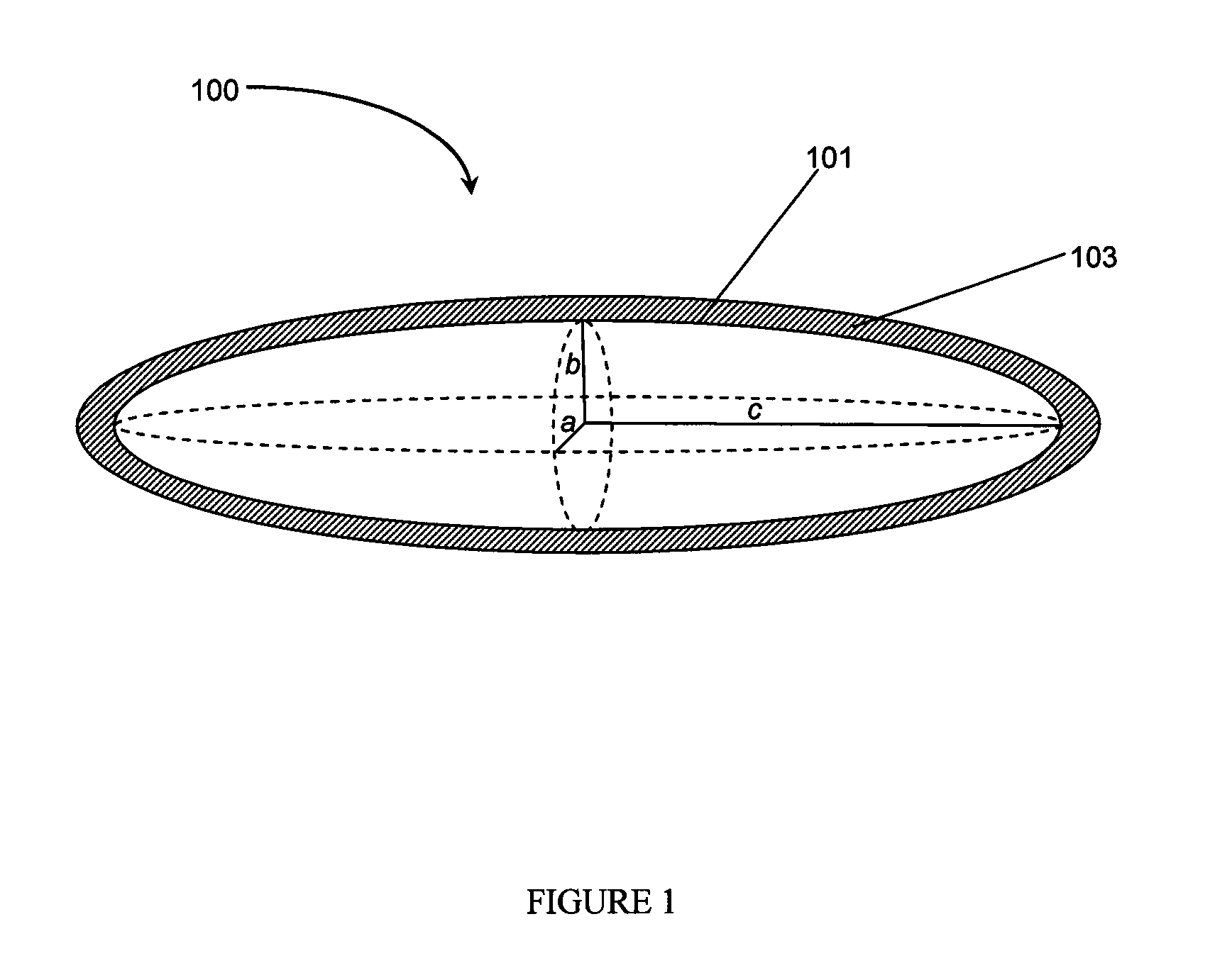
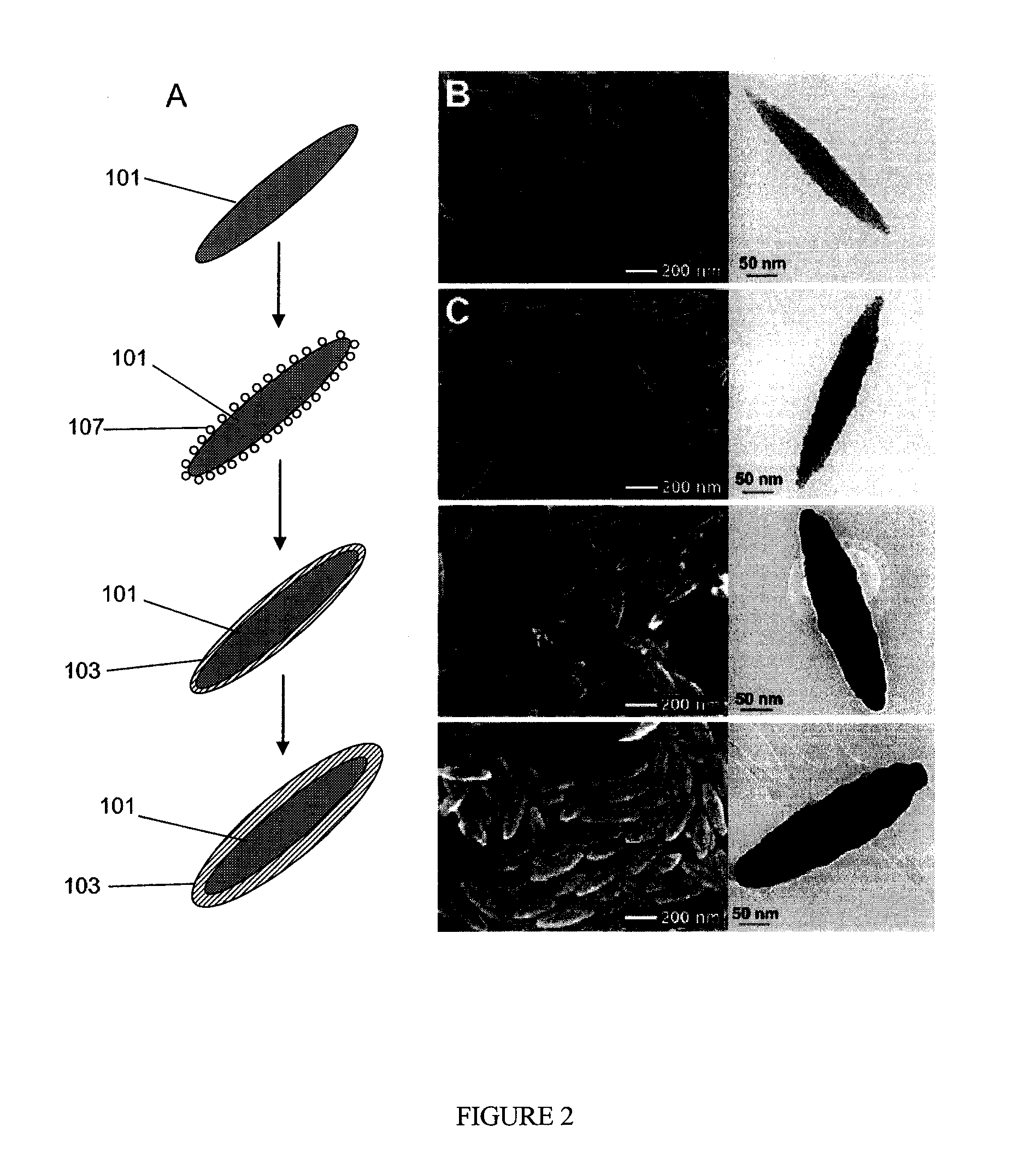
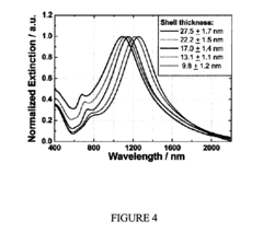
Nanorice particles: hybrid plasmonic nanostructures
PatentInactiveUS7790066B2
Innovation
- The development of nanorice particles, characterized by a prolate spheroid core coated with a conductive shell, offers enhanced structural tunability and larger local field intensity enhancements, allowing for precise control of surface plasmon resonance properties through adjustments in aspect ratios and shell thickness.
Nanostructure biosensors and systems and methods of use thereof
PatentWO2011106057A9
Innovation
- Development of label-free plasmonic nanostructure sensors using nanohole arrays that actively direct fluidics and optics for enhanced analyte delivery, allowing for direct detection of biomolecules without labels and improved sensitivity.
Fabrication Techniques for Topological Plasmonic Structures
The fabrication of topological plasmonic structures represents a critical intersection of advanced nanofabrication techniques and theoretical topological photonics principles. Current fabrication approaches can be categorized into top-down and bottom-up methodologies, each with distinct advantages for creating precise plasmonic nanostructures with topological properties.
Electron-beam lithography (EBL) remains the gold standard for top-down fabrication of topological plasmonic structures, offering sub-10 nm resolution crucial for achieving the precise geometric parameters required for topological effects. Recent advancements in EBL systems have enabled the creation of complex arrays of plasmonic meta-atoms with controlled symmetry breaking, essential for topological phase transitions in these systems.
Focused ion beam (FIB) milling provides complementary capabilities, particularly for creating three-dimensional topological plasmonic structures through selective material removal. The integration of FIB with in-situ optical characterization has significantly improved the precision of fabricating topological interfaces where plasmonic edge states can be observed.
Nanoimprint lithography has emerged as a scalable alternative, capable of replicating topological plasmonic structures over large areas. This technique has proven particularly valuable for creating extended arrays of topological plasmonic crystals where long-range order is essential for robust topological protection.
For bottom-up approaches, DNA origami templates have revolutionized the assembly of plasmonic nanoparticles into topologically non-trivial configurations. These bio-templated methods enable precise control over three-dimensional arrangements of plasmonic elements with nanometer precision, creating chiral structures that exhibit topological properties.
Colloidal self-assembly techniques have been adapted to create topological plasmonic structures through controlled aggregation processes. By engineering interparticle interactions, researchers have demonstrated the formation of quasicrystalline plasmonic arrays that support higher-order topological states.
Atomic layer deposition (ALD) plays a crucial role in fine-tuning the dielectric environment surrounding plasmonic nanostructures, allowing precise control over the coupling strength between elements in topological arrays. This technique enables the creation of topological plasmonic structures with engineered symmetry-protected topological phases.
Recent innovations in direct laser writing with two-photon polymerization have opened new possibilities for creating three-dimensional scaffolds that can be subsequently metallized to form complex topological plasmonic architectures. This approach has proven particularly valuable for creating chiral plasmonic structures with non-zero Chern numbers.
The integration of these fabrication techniques with in-situ characterization methods represents the current frontier, enabling real-time optimization of topological plasmonic structures based on their measured optical responses and topological invariants.
Quantum Effects in Topological Plasmonic Systems
The quantum realm introduces fascinating dimensions to topological plasmonic systems, where the interplay between quantum mechanics and topological protection creates novel phenomena beyond classical descriptions. At the nanoscale, quantum effects such as electron tunneling, nonlocal responses, and quantum size effects significantly alter plasmonic behavior in topologically protected structures.
Quantum confinement in topological plasmonic nanostructures leads to discrete energy levels that modify the system's optical response. This quantization becomes particularly relevant when the dimensions of plasmonic elements approach the Fermi wavelength of electrons, typically below 10 nm. In these regimes, the classical Drude model becomes insufficient, necessitating quantum-corrected models that account for electron spill-out effects and tunneling across narrow gaps.
The quantum nature of light also introduces important considerations through photon-plasmon interactions. Single-photon emitters coupled to topological plasmonic waveguides demonstrate robust transport properties resistant to backscattering from defects. These systems show promise for quantum information processing applications, where maintaining quantum coherence is paramount.
Quantum entanglement between plasmonic modes in topologically protected systems represents another frontier. Recent theoretical work suggests that topological protection can extend to quantum correlations, potentially creating decoherence-resistant quantum plasmonic circuits. Experimental verification of these predictions remains challenging but would constitute a significant breakthrough for quantum technologies.
The quantum spin Hall effect for plasmons, analogous to its electronic counterpart, enables the creation of helical edge states where plasmon propagation direction is locked to the "spin" degree of freedom. This spin-momentum locking provides natural protection against certain types of scattering and has been demonstrated in carefully designed nanostructures operating at optical frequencies.
Non-Hermitian quantum mechanics, incorporating gain and loss, introduces additional complexity to topological plasmonic systems. Exceptional points—where eigenvalues and eigenvectors coalesce—can be engineered in these systems to create novel functionalities such as enhanced sensing and unidirectional light propagation that leverage quantum effects.
Quantum fluctuations and zero-point energy considerations become relevant in topological plasmonic systems at low temperatures, potentially modifying the topological phase transitions. These quantum vacuum effects can shift the boundaries between different topological phases, requiring adjustments to the design principles established in classical regimes.
Unlock deeper insights with Patsnap Eureka Quick Research — get a full tech report to explore trends and direct your research. Try now!
Generate Your Research Report Instantly with AI Agent
Supercharge your innovation with Patsnap Eureka AI Agent Platform!