Topological Photonics in Integrated Photonic Circuit Platforms
SEP 5, 202510 MIN READ
Generate Your Research Report Instantly with AI Agent
Patsnap Eureka helps you evaluate technical feasibility & market potential.
Topological Photonics Evolution and Objectives
Topological photonics emerged as a revolutionary field at the intersection of condensed matter physics and photonics around 2008, when researchers first proposed the concept of photonic topological insulators. This field draws inspiration from topological insulators in electronic systems, where electrons can travel along the edges or surfaces without backscattering, regardless of structural imperfections. The translation of these concepts to photonic systems has opened new avenues for robust light manipulation at the nanoscale.
The evolution of topological photonics has been marked by several significant milestones. Initially, theoretical proposals dominated the landscape, with early demonstrations requiring complex metamaterials or strong magnetic fields. By 2013, researchers achieved the first experimental realizations of photonic topological insulators using arrays of coupled resonators and waveguides. The field gained substantial momentum around 2015-2017 with the demonstration of spin-Hall effects for light and valley-Hall photonic crystals, which eliminated the need for magnetic materials.
A critical turning point occurred in 2018-2020 when researchers began successfully integrating topological photonic elements into conventional integrated photonic platforms, particularly silicon photonics and III-V semiconductor platforms. This transition from proof-of-concept demonstrations to practical implementations marked the beginning of application-oriented research in this domain.
The primary objective of topological photonics in integrated circuits is to leverage topological protection to create photonic components that are inherently robust against fabrication imperfections, environmental fluctuations, and structural disorders. This robustness is particularly valuable in integrated photonics, where manufacturing variations can significantly impact device performance and yield.
Current research aims to develop practical topological photonic devices that can outperform conventional counterparts in specific metrics, such as insertion loss, bandwidth, and temperature stability. The field is working toward creating topologically protected waveguides, resonators, and beam splitters that maintain consistent performance across varying conditions.
Long-term objectives include the development of large-scale topological photonic integrated circuits (PICs) that combine multiple topological elements to perform complex functions with unprecedented reliability. Researchers are also exploring the integration of topological photonics with other emerging technologies, such as quantum photonics, to create fault-tolerant quantum information processing platforms.
Another important goal is to establish standardized design methodologies and fabrication processes that would enable the commercial adoption of topological photonic components in telecommunications, data centers, and sensing applications. The ultimate vision is to create a new generation of photonic integrated circuits where topological protection becomes a standard design principle rather than an exotic physical phenomenon.
Market Analysis for Integrated Photonic Circuits
The integrated photonic circuits (IPCs) market is experiencing robust growth, driven by increasing demand for high-speed data transmission, telecommunications infrastructure expansion, and emerging applications in quantum computing. Current market valuations place the global IPC sector at approximately 3.5 billion USD in 2023, with projections indicating a compound annual growth rate of 21% through 2030, potentially reaching 15 billion USD by the end of the decade.
Telecommunications remains the dominant application segment, accounting for nearly 40% of the total market share. Data centers represent the fastest-growing segment with 28% annual growth, as operators seek energy-efficient solutions to manage exponentially increasing data traffic. The integration of topological photonics into these circuits presents a significant market opportunity, particularly for applications requiring robust performance under manufacturing variations and environmental perturbations.
Geographically, North America leads the market with 38% share, followed by Asia-Pacific at 35% and Europe at 22%. China and Taiwan have emerged as manufacturing powerhouses, while research and development remains concentrated in the United States, Japan, and Western Europe. The Asia-Pacific region is expected to demonstrate the highest growth rate over the next five years due to substantial investments in telecommunications infrastructure and government initiatives supporting photonics research.
From a customer perspective, the market exhibits a bifurcated structure. Large telecommunications equipment manufacturers and data center operators constitute the primary customer base, valuing performance and reliability over cost considerations. A secondary market segment comprises research institutions and specialized technology companies exploring novel applications in quantum computing, biosensing, and artificial intelligence, where topological photonic properties offer unique advantages.
Supply chain analysis reveals increasing vertical integration among major players, with companies like Intel, IBM, and NTT expanding their capabilities across the value chain. This trend is partially driven by the need to control critical manufacturing processes for topological photonic structures, which require precise fabrication techniques beyond standard photolithography.
Pricing trends indicate gradual cost reduction as manufacturing processes mature, with current premium pricing for topological photonic components expected to normalize within 3-5 years. The cost trajectory follows patterns similar to other semiconductor technologies, with significant economies of scale anticipated once production volumes increase.
Market barriers include high initial capital requirements, complex manufacturing processes, and the need for specialized expertise in both photonics and topological physics. These factors currently limit market entry to well-established companies and well-funded startups with strong academic connections. However, the emergence of foundry services specializing in photonic integrated circuits is gradually lowering these barriers, potentially accelerating market adoption of topological photonic technologies.
Current Challenges in Topological Photonic Integration
Despite significant advancements in topological photonics research, the integration of topological photonic concepts into practical integrated photonic circuits faces several substantial challenges. The fundamental issue lies in the translation of theoretical topological protection mechanisms to nanoscale photonic platforms that are compatible with existing semiconductor fabrication processes. Current silicon photonics and III-V platforms exhibit material constraints that limit the implementation of certain topological effects, particularly those requiring strong magneto-optical responses or complex three-dimensional structures.
Fabrication precision represents another critical hurdle. Topological photonic devices often require precise geometric arrangements with nanometer-scale accuracy to maintain their topological properties. Even minor deviations in fabrication can disrupt the band structure and compromise topological protection. This challenge is particularly acute for devices operating at telecommunications wavelengths, where feature sizes must be controlled with exceptional precision.
The scalability of topological photonic systems presents significant integration difficulties. While laboratory demonstrations have shown promising results in isolated components, scaling these designs to complex integrated circuits with multiple topological elements remains problematic. The interfaces between topological and conventional photonic components often introduce losses and reflections that undermine the benefits of topological protection.
Energy efficiency concerns also plague current implementations. Many topological photonic designs require complex structures that introduce additional propagation losses or require active components with high power consumption. This contradicts the industry trend toward low-power photonic integrated circuits for data centers and telecommunications applications.
Testing and characterization methodologies for topological photonic devices remain underdeveloped. Conventional optical testing approaches often fail to adequately measure the unique properties of topological states, such as robustness against certain classes of defects while maintaining sensitivity to others. This complicates quality control and performance verification in manufacturing environments.
The temperature sensitivity of topological photonic structures presents another significant challenge. Many designs exhibit performance degradation under thermal fluctuations, limiting their practical deployment in variable environmental conditions. This is particularly problematic for data center applications where temperature management is already a critical concern.
Finally, the theoretical-practical gap remains substantial. While theoretical proposals for topological photonic devices abound in academic literature, translating these concepts into manufacturable designs with clear performance advantages over conventional approaches requires significant engineering development. The lack of standardized design methodologies and simulation tools specifically optimized for topological photonics further complicates this translation process.
Existing Implementations of Topological Photonic Circuits
01 Topological photonic structures and devices
Topological photonics involves designing structures that support robust light propagation through topologically protected states. These structures include photonic crystals, metamaterials, and waveguides engineered to exhibit topological properties. The topological protection enables light to propagate without backscattering at sharp bends or around defects, making these devices highly efficient for optical signal routing and processing applications.- Topological photonic crystals and waveguides: Topological photonic crystals and waveguides utilize topological protection principles to create robust light propagation paths that are immune to backscattering from defects and sharp bends. These structures implement photonic analogs of quantum Hall effect and topological insulators, featuring edge states that allow unidirectional light propagation. The topological protection enables efficient waveguiding even around sharp corners and in the presence of manufacturing imperfections, making them valuable for integrated photonic circuits and optical communication systems.
- Topological lasers and optical amplifiers: Topological lasers and optical amplifiers leverage topological protection to enhance performance and stability. These devices incorporate topological insulator principles into gain media structures to create robust lasing modes that are resistant to fabrication defects and environmental perturbations. The topologically protected modes enable single-mode operation, reduced threshold, and improved beam quality. These innovations lead to more efficient and stable light sources for applications in optical communications, sensing, and quantum information processing.
- Quantum topological photonics: Quantum topological photonics combines quantum optics with topological protection to create novel platforms for quantum information processing. These systems utilize topologically protected states to transport and manipulate quantum information with reduced decoherence and loss. By engineering photonic structures with non-trivial topology, quantum states can be processed more reliably, enabling applications in quantum computing, quantum simulation, and secure quantum communication networks. The topological protection helps preserve quantum coherence against environmental noise and fabrication imperfections.
- Topological photonic metamaterials: Topological photonic metamaterials are artificially engineered structures that exhibit exotic optical properties through topological band structures. These materials feature carefully designed unit cells that create photonic bandgaps with topologically protected edge states. By controlling the geometry and composition of these metamaterials, researchers can achieve unusual light-matter interactions, including negative refraction, super-resolution imaging, and cloaking effects. These metamaterials enable manipulation of electromagnetic waves in ways not possible with conventional materials, opening new possibilities for optical devices and systems.
- Topological photonics for telecommunications: Topological photonics offers significant advantages for telecommunications systems through robust light routing and signal processing. By implementing topologically protected waveguides and resonators in optical communication networks, signal integrity can be maintained despite physical imperfections in the transmission path. These systems enable more efficient multiplexing, switching, and routing of optical signals with reduced crosstalk and insertion loss. The inherent stability of topological photonic devices makes them particularly valuable for high-bandwidth, long-distance optical communications and data center interconnects.
02 Quantum applications of topological photonics
Topological photonic systems are being integrated with quantum information processing to create robust quantum optical circuits. These systems leverage topological protection to maintain quantum coherence and reduce decoherence effects. Applications include quantum computing, quantum communication networks, and quantum sensing technologies that benefit from the inherent stability of topologically protected light states.Expand Specific Solutions03 Topological edge states and waveguides
Topological photonic systems support special edge states at interfaces between regions with different topological properties. These edge states enable unidirectional light propagation that is immune to backscattering from defects or disorder. Researchers are developing waveguides that utilize these edge states for efficient light transport in integrated photonic circuits, with applications in telecommunications and optical computing.Expand Specific Solutions04 Fabrication methods for topological photonic devices
Advanced fabrication techniques are being developed to create topological photonic structures at various scales. These methods include nanolithography, 3D printing, self-assembly processes, and precision etching techniques. The fabrication approaches aim to create precise periodic structures with controlled defects or interfaces that exhibit the desired topological properties for manipulating light propagation.Expand Specific Solutions05 Integration of topological photonics with other technologies
Topological photonic principles are being integrated with other technological platforms to create hybrid systems with enhanced functionality. These include integration with electronic circuits for optoelectronic applications, combination with plasmonic structures for subwavelength light manipulation, and incorporation into fiber optic systems for telecommunications. The integration enables new capabilities in sensing, signal processing, and information technology.Expand Specific Solutions
Leading Research Groups and Companies in Topological Photonics
Topological photonics in integrated photonic circuit platforms is emerging as a transformative technology, currently in its early growth phase. The market is expanding rapidly, projected to reach significant scale as photonic integrated circuits become essential for next-generation computing and communications. While still evolving toward full commercial maturity, key players are driving innovation across different segments. Industry leaders like IBM, Intel, and TSMC are developing manufacturing capabilities, while specialized photonics companies such as EFFECT Photonics and Rockley Photonics focus on commercial applications. Academic institutions including Peking University, Zhejiang University, and University of Maryland contribute fundamental research. The ecosystem demonstrates a balanced mix of established technology corporations, specialized photonics firms, and research institutions collaborating to advance this promising field.
International Business Machines Corp.
Technical Solution: IBM has developed advanced topological photonic circuits that leverage the robustness of topological edge states to create light pathways immune to manufacturing defects and environmental perturbations. Their approach integrates silicon photonics with topological waveguides to create protected optical channels that maintain signal integrity even in the presence of sharp bends or defects. IBM's research focuses on creating topologically protected ring resonators and waveguide arrays that can be integrated into their existing silicon photonics platform. They've demonstrated successful implementation of photonic quantum walks using topological structures, enabling more reliable quantum information processing. IBM has also pioneered the use of synthetic dimensions in integrated photonic circuits, allowing for higher-dimensional topological physics to be explored in a planar chip architecture[1][3].
Strengths: IBM's extensive silicon photonics manufacturing infrastructure enables rapid prototyping and scaling of topological photonic designs. Their approach offers exceptional robustness against fabrication imperfections, which is critical for mass production. Weaknesses: Their topological designs often require complex structures with precise dimensional control, increasing fabrication complexity and potentially limiting yield in commercial applications.
Intel Corp.
Technical Solution: Intel has developed a comprehensive topological photonics platform based on their silicon photonics technology. Their approach focuses on creating valley-Hall topological insulators in silicon nitride waveguide arrays, enabling robust light propagation along interfaces between topologically distinct regions. Intel's platform incorporates reconfigurable topological photonic circuits using thermo-optic phase shifters, allowing dynamic control of topological properties. They've demonstrated practical applications including robust optical delay lines, high-efficiency optical switches, and topologically protected beam splitters. Intel's research also extends to higher-order topological insulators that support corner states with extreme light localization, useful for sensing applications. Their technology leverages existing silicon photonics manufacturing processes, making it compatible with their electronic-photonic integration roadmap[2][5].
Strengths: Intel's approach seamlessly integrates with CMOS manufacturing processes, enabling cost-effective mass production. Their reconfigurable platform offers versatility for multiple applications in data communications. Weaknesses: The thermal tuning mechanisms used for reconfigurability increase power consumption and limit switching speed compared to purely electronic approaches.
Key Patents and Breakthroughs in Topological Protection
Photonic integrated circuit platform and optical phase array device using the same
PatentActiveUS12174416B2
Innovation
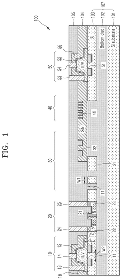
- The proposed solution involves a photonic integrated circuit platform with a substrate, multiple oxide layers, and optical element layers, including semiconductor and compound semiconductor materials, where silicon nitride is used as an insulating material to reduce optical loss and enhance thermal conductivity, and the structure is designed to facilitate vertical evanescent coupling between optical waveguides for efficient light transmission.
Integration of an active component on a photonics platform
PatentInactiveUS20220075112A1
Innovation
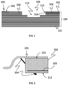
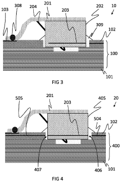
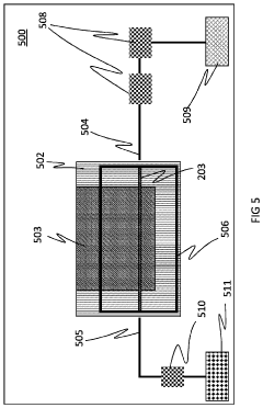
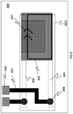
- A photonics integrated circuit design featuring a recessed substrate with a parallel surface for lateral optical coupling, combined with a wiring substrate for precise electrical connectivity and thermal management, allowing for hybrid integration of active components with improved alignment and reduced material incompatibility issues.
Fabrication Techniques for Topological Photonic Structures
The fabrication of topological photonic structures represents a critical challenge in translating theoretical concepts into practical integrated photonic circuits. Current fabrication techniques leverage both established semiconductor processing methods and emerging nanofabrication approaches to realize these complex structures with the precision required for topological protection.
Conventional lithographic techniques, including electron-beam lithography (EBL) and deep-UV photolithography, serve as primary methods for patterning topological photonic crystals and waveguides. EBL offers nanometer-scale resolution crucial for creating precise lattice structures with engineered symmetry breaking, while deep-UV lithography enables larger-scale production with sub-100nm resolution. These techniques are particularly effective when implemented on silicon-on-insulator (SOI) platforms, which have become the standard for integrated photonics.
Advanced etching processes complement lithographic patterning, with reactive ion etching (RIE) and inductively coupled plasma (ICP) etching providing the anisotropic profiles necessary for vertical sidewalls in photonic crystal structures. The precise control of etch depth and sidewall angle is essential for maintaining the designed band structure that enables topological protection.
For more complex three-dimensional topological structures, multi-layer fabrication approaches have been developed. These involve sequential deposition, patterning, and etching steps with precise alignment between layers. Direct laser writing using two-photon polymerization has emerged as a promising alternative for creating 3D structures, offering design flexibility though with limited throughput.
Material selection plays a crucial role in fabrication strategy. Silicon, silicon nitride, and III-V semiconductors remain dominant due to their favorable optical properties and compatibility with established fabrication processes. Recent innovations include the incorporation of phase-change materials and magneto-optical materials to enable dynamic tuning of topological properties.
Precision control of dimensional parameters presents significant challenges, as topological properties often depend sensitively on geometric details. Advanced metrology techniques, including scanning electron microscopy and atomic force microscopy, are routinely employed to verify structural fidelity. Post-fabrication trimming using focused ion beam milling or laser-assisted processes helps achieve the required precision.
Scalable manufacturing remains an ongoing challenge, with current research focusing on adapting topological designs to be compatible with foundry processes. This includes developing designs that maintain topological protection despite fabrication variations, and implementing self-correction mechanisms that leverage the inherent robustness of topological states.
Quantum Applications of Topological Photonic Circuits
Quantum Applications of Topological Photonic Circuits
Topological photonic circuits represent a revolutionary frontier in quantum information processing, offering robust light manipulation capabilities that are inherently protected against manufacturing imperfections and environmental perturbations. The quantum applications of these systems leverage their unique ability to support edge states that propagate with minimal backscattering, creating ideal conditions for quantum operations that require high coherence.
One of the most promising quantum applications is in the development of topologically protected quantum light sources. By integrating quantum emitters with topological waveguides, researchers have demonstrated enhanced emission rates and directional coupling of single photons. These topologically protected single-photon sources exhibit remarkable resilience against disorder-induced scattering, addressing a critical challenge in scalable quantum photonic technologies.
Topological photonic circuits also show exceptional potential for quantum simulation. The ability to engineer synthetic gauge fields and complex Hamiltonians in these platforms enables the simulation of quantum many-body systems that are otherwise computationally intractable. Recent experiments have successfully simulated topological phases of matter and exotic quantum phenomena, providing insights into fundamental physics while establishing a pathway toward practical quantum advantage.
In quantum communication, topological protection offers significant advantages for maintaining quantum coherence over extended distances. Researchers have demonstrated that quantum states encoded in topological edge modes can propagate with significantly reduced decoherence compared to conventional waveguides. This property is particularly valuable for chip-scale quantum key distribution systems and quantum repeater networks, where maintaining quantum information integrity is paramount.
The integration of topological photonics with superconducting quantum circuits represents another frontier application. Hybrid systems combining topological photonic waveguides with superconducting qubits benefit from both the robust light transport of topological photonics and the strong nonlinearities of superconducting elements. These hybrid platforms show promise for implementing fault-tolerant quantum logic gates and quantum error correction protocols.
Looking toward practical implementation, several research groups have recently demonstrated topologically protected quantum interference on silicon photonic platforms. These experiments showcase the potential for performing robust quantum operations in integrated circuits that can be manufactured using established semiconductor fabrication techniques, bringing topological quantum photonics closer to technological readiness.
Unlock deeper insights with Patsnap Eureka Quick Research — get a full tech report to explore trends and direct your research. Try now!
Generate Your Research Report Instantly with AI Agent
Supercharge your innovation with Patsnap Eureka AI Agent Platform!
