Reconfigurable Metasurfaces for Topological Photonic Control
SEP 5, 20259 MIN READ
Generate Your Research Report Instantly with AI Agent
Patsnap Eureka helps you evaluate technical feasibility & market potential.
Metasurface Technology Evolution and Objectives
Metasurfaces represent a revolutionary class of engineered surfaces composed of subwavelength structures that can manipulate electromagnetic waves in unprecedented ways. The evolution of metasurface technology has undergone significant transformation since its conceptual emergence in the early 2000s, evolving from static designs with fixed functionalities to today's reconfigurable platforms that enable dynamic control over electromagnetic properties.
The initial development phase (2000-2010) focused primarily on proof-of-concept demonstrations with passive metasurfaces, where researchers established fundamental principles for wavefront manipulation through phase, amplitude, and polarization control. These early designs, while groundbreaking, were inherently limited by their static nature.
The second evolutionary phase (2010-2015) saw the integration of active components into metasurface designs, enabling limited tunability through external stimuli such as electrical signals, thermal inputs, or mechanical deformation. This period marked the transition from purely passive to semi-active metasurface technologies.
The current phase (2015-present) has witnessed remarkable advancement toward fully reconfigurable metasurfaces, incorporating materials with tunable electromagnetic properties such as liquid crystals, phase-change materials, and 2D materials like graphene. These developments have enabled real-time control over metasurface functionalities, opening pathways to programmable electromagnetic environments.
Topological photonics emerged as a parallel development, inspired by concepts from condensed matter physics. The integration of topological principles with metasurfaces represents a cutting-edge frontier, promising robust light manipulation immune to fabrication imperfections and environmental perturbations.
The primary objectives for reconfigurable metasurfaces in topological photonic control include achieving dynamic manipulation of topologically protected states, developing platforms for topological phase transitions on demand, and creating systems capable of real-time reconfiguration of topological invariants.
Additional technical goals encompass increasing operational bandwidth, enhancing modulation speed, improving energy efficiency, and developing scalable fabrication techniques compatible with existing semiconductor manufacturing processes. The ultimate vision is to create programmable metasurfaces that can dynamically control topological photonic properties with high precision and reliability.
The convergence of reconfigurable metasurfaces with topological photonics aims to revolutionize applications in quantum information processing, robust optical communication systems, and next-generation computing architectures by leveraging the unique advantages of topologically protected light propagation with the flexibility of dynamic reconfigurability.
Market Applications for Reconfigurable Photonic Control
Reconfigurable metasurfaces for topological photonic control represent a transformative technology with diverse market applications across multiple industries. The telecommunications sector stands as a primary beneficiary, where these advanced surfaces enable dynamic beam steering and wavefront shaping for next-generation wireless communications. This capability directly addresses the growing demand for high-bandwidth, low-latency connections in 5G and future 6G networks, potentially increasing network capacity by optimizing signal propagation in complex environments.
In the medical imaging field, reconfigurable metasurfaces offer unprecedented control over electromagnetic waves, enabling higher resolution imaging techniques and potentially revolutionizing non-invasive diagnostic tools. The ability to manipulate light at the subwavelength scale translates to sharper images and detection of smaller abnormalities, significantly enhancing early disease detection capabilities.
The aerospace and defense sectors have shown substantial interest in this technology for radar systems and secure communications. Metasurface-enhanced radar can achieve superior target discrimination and reduced vulnerability to jamming, while reconfigurable features allow for adaptive responses to changing operational conditions. Market analysts project this segment to grow rapidly as defense modernization programs increasingly incorporate advanced electromagnetic technologies.
Consumer electronics represents another promising market, particularly for augmented reality (AR) and virtual reality (VR) applications. Reconfigurable metasurfaces can enable thinner, lighter optical components with dynamic focusing capabilities, addressing key limitations in current AR/VR displays. This technology could help reduce device form factors while improving visual quality and reducing eye strain.
The automotive industry is exploring applications in sensing systems for autonomous vehicles, where metasurfaces could enhance LiDAR performance by enabling adaptive beam steering and improved signal processing in varying environmental conditions. This capability directly addresses current challenges in all-weather perception systems.
Energy harvesting applications are emerging as metasurfaces demonstrate potential for improving solar cell efficiency through enhanced light trapping and spectrum conversion. The reconfigurability aspect allows for dynamic optimization based on changing light conditions, potentially increasing energy capture throughout the day.
Manufacturing sectors are investigating metasurface applications for quality control and non-destructive testing, where precise control of electromagnetic waves enables detection of internal defects in materials and components that would otherwise remain hidden to conventional inspection methods.
Topological Photonics: Current State and Barriers
Topological photonics represents a rapidly evolving frontier in optical science, leveraging principles from topological physics to manipulate light in unprecedented ways. Currently, the field has achieved significant milestones, including the experimental demonstration of photonic topological insulators, robust waveguides, and topologically protected edge states. These advances have enabled light propagation that remains immune to certain types of defects and backscattering, offering potential breakthroughs for optical communication and quantum information processing.
Despite these achievements, several substantial barriers impede further development in topological photonics, particularly in the context of reconfigurable metasurfaces. The most significant challenge remains the limited reconfigurability of topological photonic structures. While static topological systems are well-established, creating dynamically tunable topological properties presents formidable difficulties due to the inherent stability of topological states.
Material constraints constitute another major obstacle. Current materials used in metasurfaces often lack the necessary combination of optical properties, tunability, and fabrication compatibility required for effective topological control. The trade-off between material response time and topological protection quality continues to challenge researchers seeking practical applications.
Fabrication precision represents a critical bottleneck. Topological photonic systems typically require nanoscale precision in their geometric arrangements, with even minor deviations potentially disrupting the desired topological properties. This precision requirement becomes exponentially more challenging when incorporating reconfigurable elements into metasurface designs.
The theoretical-experimental gap further complicates progress. While theoretical models predict numerous fascinating topological photonic phenomena, experimental verification remains elusive for many concepts due to technological limitations. This discrepancy slows the translation of theoretical advances into practical applications.
Energy efficiency concerns also present significant barriers. Many current approaches to reconfigurable metasurfaces require substantial energy input for tuning, limiting their practicality for low-power applications and integrated photonic systems. The power requirements for maintaining topological states in dynamic systems can be prohibitively high.
Finally, integration challenges with existing photonic technologies hinder widespread adoption. Topological photonic systems often employ unique geometries and operational principles that do not readily interface with conventional optical components, creating compatibility issues that must be resolved before commercial applications become viable.
Overcoming these barriers will require interdisciplinary approaches combining advances in material science, nanofabrication, theoretical physics, and engineering to realize the full potential of reconfigurable metasurfaces for topological photonic control.
Current Approaches to Reconfigurable Metasurfaces
01 Reconfigurable metasurfaces for dynamic wavefront control
Reconfigurable metasurfaces enable dynamic control of electromagnetic wavefronts through tunable elements that can be adjusted in real-time. These metasurfaces incorporate active components such as liquid crystals, phase-change materials, or MEMS structures that allow for manipulation of phase, amplitude, and polarization of light. By dynamically altering the optical properties of the metasurface, these systems can perform functions like beam steering, focusing, and holographic projection with programmable control.- Reconfigurable metasurfaces for dynamic wavefront control: Reconfigurable metasurfaces enable dynamic control of electromagnetic wavefronts through tunable elements that can modify phase, amplitude, and polarization in real-time. These structures incorporate active components such as liquid crystals, phase-change materials, or MEMS that respond to external stimuli like voltage, temperature, or optical signals. The ability to dynamically reconfigure the optical properties allows for adaptive beam steering, focusing, and holographic applications without mechanical movement, making them valuable for advanced optical systems and communications.
- Topological photonic structures for robust light propagation: Topological photonic structures leverage topological protection principles to create robust light propagation channels that resist backscattering and are immune to certain types of defects or disorder. These structures implement photonic analogs of topological insulators, featuring protected edge states that enable unidirectional light propagation. By engineering the band structure and symmetry properties of photonic crystals or metamaterials, these systems create topologically protected optical pathways that maintain consistent performance even in the presence of fabrication imperfections or environmental variations.
- Integration of active materials for tunable metasurface properties: Active materials are integrated into metasurface designs to achieve tunable optical properties. These materials include phase-change materials, 2D materials like graphene, liquid crystals, and semiconductors with carrier-dependent optical responses. When subjected to external stimuli such as electrical signals, optical pumping, or thermal changes, these materials undergo significant changes in their electromagnetic properties. This integration enables switching between different operational modes, continuous tuning of resonance frequencies, and programmable control of light-matter interactions at the subwavelength scale.
- Computational design methods for metasurface optimization: Advanced computational methods are employed to design and optimize metasurfaces for specific topological photonic applications. These approaches include inverse design algorithms, machine learning techniques, and topology optimization that can efficiently navigate the vast design space of metasurface structures. By defining target optical responses and constraints, these computational tools can generate non-intuitive geometries and arrangements of meta-atoms that achieve desired functionalities. The methods enable rapid prototyping and optimization of complex metasurface designs that would be difficult to develop through conventional approaches.
- Applications in optical communications and sensing systems: Reconfigurable metasurfaces with topological properties are applied in advanced optical communications and sensing systems. These applications include beam steering for LiDAR and free-space optical communications, tunable filters for spectroscopy, programmable holograms for 3D displays, and adaptive optics for imaging through turbulent media. The combination of reconfigurability and topological protection enables robust performance in variable environments while maintaining high efficiency. These technologies are particularly valuable for next-generation wireless communications, autonomous vehicles, biomedical imaging, and quantum information processing systems.
02 Topological photonic structures for robust light propagation
Topological photonic structures leverage principles from topological physics to create protected optical states that are robust against defects and disorder. These structures utilize carefully designed geometric arrangements of optical elements to create photonic bandgaps and edge states that allow light to propagate with minimal loss around sharp corners and through imperfections. The topological protection ensures stable light propagation paths that are immune to backscattering and environmental perturbations, making them ideal for reliable photonic circuits and waveguides.Expand Specific Solutions03 Integration of active materials for tunable metasurfaces
Active materials are integrated into metasurface designs to achieve tunability and reconfigurability. These materials include phase-change materials, graphene, liquid crystals, and semiconductors that can change their optical properties in response to external stimuli such as electrical signals, temperature changes, or optical excitation. The integration enables switching between different operational modes, continuous tuning of resonance frequencies, and adaptive control of light-matter interactions, significantly enhancing the functionality of metasurface devices for applications in communications, sensing, and imaging.Expand Specific Solutions04 Computational design and optimization of topological photonic metasurfaces
Advanced computational methods are employed to design and optimize topological photonic metasurfaces. These approaches include inverse design algorithms, machine learning techniques, and topology optimization that can efficiently explore vast design spaces to achieve desired optical functionalities. The computational frameworks enable the discovery of non-intuitive metasurface geometries that maximize performance metrics such as efficiency, bandwidth, and angular tolerance while satisfying fabrication constraints. These methods significantly accelerate the development cycle of novel metasurface devices with unprecedented capabilities.Expand Specific Solutions05 Applications of reconfigurable topological metasurfaces
Reconfigurable topological metasurfaces find applications across multiple domains including telecommunications, quantum information processing, sensing, and imaging. These applications leverage the unique properties of topological protection combined with dynamic reconfigurability to create robust optical systems that can adapt to changing requirements. Specific implementations include tunable optical filters, programmable beam formers for LIDAR systems, reconfigurable holograms, adaptive optical elements for imaging through turbulent media, and components for quantum optical circuits that require precise control of photon propagation paths.Expand Specific Solutions
Leading Research Groups and Industry Stakeholders
Reconfigurable Metasurfaces for Topological Photonic Control is currently in an early growth phase, with increasing research interest but limited commercial applications. The market is expanding rapidly, projected to reach significant scale as applications in telecommunications, sensing, and quantum computing mature. Technologically, academic institutions like Wuhan University, Harvard College, and Zhejiang University are leading fundamental research, while companies such as Intel Corp. and Fujikura Ltd. are beginning to explore practical implementations. Metahelios Ltd. represents one of the few specialized startups commercializing metasurface technology. The field is transitioning from theoretical exploration to prototype development, with international collaboration between research institutions in China, the US, and Europe accelerating innovation in reconfigurable topological photonic systems.
President & Fellows of Harvard College
Technical Solution: Harvard has pioneered reconfigurable metasurfaces with their phase-change material integration approach. Their technical solution involves embedding phase-change materials (like GST) within metasurface structures to enable dynamic control of electromagnetic wave properties. Harvard researchers have developed metasurfaces that can be reconfigured through thermal, electrical, or optical stimuli to modify their topological properties on demand. Their platform demonstrates the ability to dynamically switch between different topological phases, enabling protected waveguiding and robust light manipulation even in the presence of defects and disorder. The Harvard approach particularly excels in creating reconfigurable topological edge states that can be turned on and off or redirected in real-time, offering unprecedented control over light propagation paths[1][3].
Strengths: Superior integration of phase-change materials with metasurfaces enabling multi-state reconfigurability; exceptional precision in topological phase transitions; strong intellectual property portfolio. Weaknesses: Complex fabrication processes limiting mass production; relatively high power requirements for thermal reconfiguration; challenges in scaling down device dimensions.
The Regents of the University of California
Technical Solution: UC's technical solution centers on MEMS-based reconfigurable metasurfaces for topological photonic control. Their approach incorporates microelectromechanical systems directly into metasurface architectures, allowing physical reconfiguration of the meta-atoms through electrostatic actuation. This enables dynamic modification of the photonic band structure and topological invariants. UC researchers have demonstrated metasurfaces with tunable valley-Hall effects where mechanical deformation of the metasurface structure induces transitions between topologically distinct phases. Their platform achieves reconfiguration speeds in the microsecond range while maintaining the topological protection of edge states. The UC system incorporates addressable arrays of MEMS actuators to create programmable topological pathways for light, enabling complex wavefront shaping and beam steering with topological protection against backscattering[2][5].
Strengths: High-speed reconfiguration capabilities; excellent mechanical durability; compatibility with existing semiconductor fabrication processes. Weaknesses: Limited reconfiguration range compared to other approaches; mechanical wear concerns for long-term reliability; higher complexity in control systems for large-scale arrays.
Key Patents in Topological Photonic Control
Dynamically reconfigurable optical metasurfaces
PatentPendingUS20240385468A1
Innovation
- The use of a dynamic optical metasurface comprising a substrate and a phase change material (PCM) film, which can be optically programmed to have a varying index of refraction in the infrared spectrum, is employed. This involves depositing an amorphous PCM film on a substrate, exposing it to laser radiation to convert it to a crystalline state, and cycling between these states to modulate the refractive index, while also forming nanostructured pillars and annealing them to create a spatially varied PCM phase metasurface.
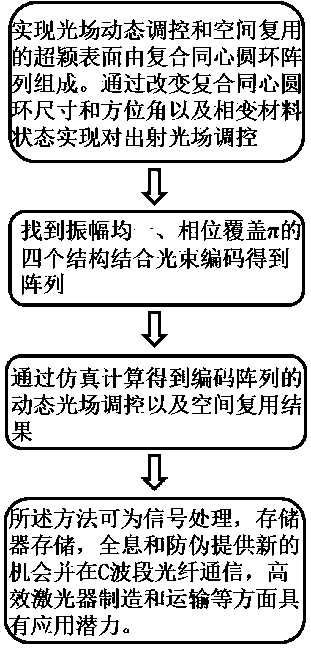
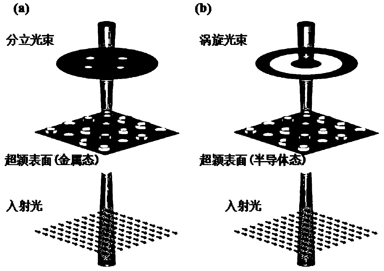
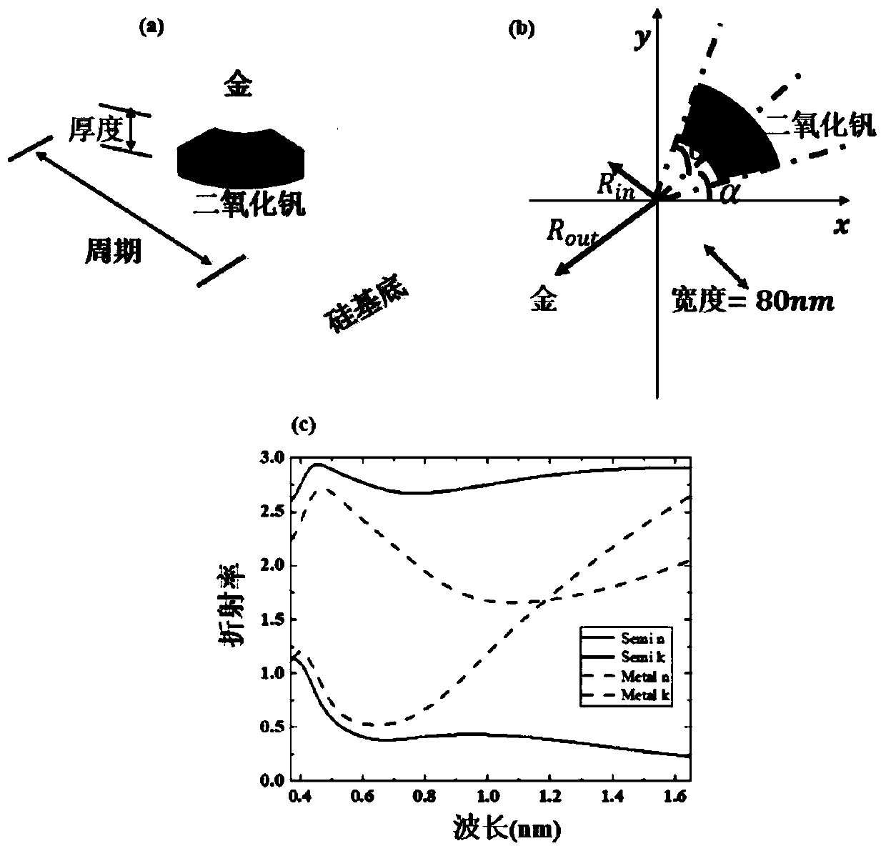
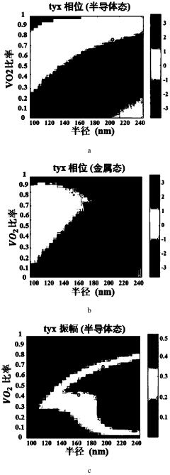
Optical field dynamic modulation and spatial multiplexing method based on reconfigurable hybrid metasurface
PatentActiveCN110096781A
Innovation
- Using a light field dynamic modulation and spatial multiplexing method based on reconfigurable hybrid metasurfaces, through a composite circular ring structure array of different geometric sizes and symmetry axes, the state changes of phase change materials are used to achieve dynamic control and control of the incident beam. Spatial multiplexing includes changing the outer diameter, phase change material proportion and symmetry axis direction of the composite ring structure to achieve arbitrary control of the amplitude and phase of the outgoing beam.
Fabrication Techniques and Material Considerations
The fabrication of reconfigurable metasurfaces for topological photonic control requires sophisticated techniques and careful material selection to achieve the desired electromagnetic properties and reconfigurability. Traditional nanofabrication methods such as electron-beam lithography (EBL) and focused ion beam (FIB) milling remain fundamental for creating precise nanostructures with feature sizes below 100 nm, which are essential for metasurfaces operating at optical frequencies.
Advanced techniques like direct laser writing and nanoimprint lithography have emerged as scalable alternatives, offering higher throughput for commercial applications while maintaining nanoscale precision. For dynamic reconfigurability, complementary metal-oxide-semiconductor (CMOS) compatible processes have gained prominence, enabling integration with existing electronic systems and facilitating active control mechanisms.
Material selection critically influences both the performance and reconfigurability of topological metasurfaces. Phase-change materials (PCMs) like Ge2Sb2Te5 (GST) exhibit significant refractive index changes upon phase transitions, making them excellent candidates for reconfigurable designs. These materials can be switched between amorphous and crystalline states using thermal, electrical, or optical stimuli, providing a robust mechanism for altering topological properties on demand.
Liquid crystals represent another promising material platform, offering continuous tuning of optical properties through electric field manipulation. Their integration with metasurfaces has demonstrated effective control over topological states, though challenges remain in response time and operating conditions.
Two-dimensional materials, particularly graphene and transition metal dichalcogenides (TMDs), have revolutionized reconfigurable metasurface design due to their exceptional electro-optical properties and atomic thinness. Graphene's tunable conductivity through electrostatic gating enables active control of surface plasmons, while TMDs offer strong light-matter interactions and valley-selective responses crucial for topological photonics.
Hybrid material systems combining plasmonic metals (gold, silver) with active dielectrics have shown enhanced performance by leveraging the strengths of each component. These composites can achieve stronger light-matter interactions while maintaining dynamic tunability.
Fabrication challenges persist in achieving precise alignment between multiple layers, maintaining material quality during processing, and ensuring uniform properties across large areas. Recent innovations in atomic layer deposition and self-assembly techniques show promise in addressing these limitations, potentially enabling cost-effective manufacturing of complex topological metasurfaces with consistent performance characteristics.
Integration Challenges with Existing Photonic Systems
The integration of reconfigurable metasurfaces with existing photonic systems presents significant technical challenges that must be addressed to realize their full potential in topological photonic control applications. Current photonic integrated circuits (PICs) and optical communication systems have been optimized over decades with standardized components and interfaces, creating compatibility hurdles for novel metasurface technologies. The dimensional mismatch between conventional photonic waveguides (typically hundreds of nanometers) and metasurface structures (often operating at wavelength scales) necessitates sophisticated mode conversion and coupling mechanisms.
Signal integrity represents another critical challenge, as the introduction of metasurfaces into established optical paths can generate unwanted reflections, scattering, and mode conversion effects that degrade overall system performance. These effects become particularly problematic in high-speed data transmission systems where signal fidelity is paramount. Furthermore, the dynamic reconfiguration capabilities of these metasurfaces introduce temporal considerations that conventional photonic systems are not designed to accommodate.
Fabrication compatibility presents additional obstacles, as metasurfaces often require specialized manufacturing processes that may not align with standard photonic fabrication techniques. The integration of electronic control circuitry necessary for reconfiguration further complicates the manufacturing process, requiring careful consideration of thermal management and electromagnetic interference issues. Many existing photonic systems utilize materials like silicon, silicon nitride, or III-V semiconductors, while advanced metasurfaces may incorporate phase-change materials, liquid crystals, or 2D materials with different processing requirements.
Power consumption and thermal management emerge as significant concerns when integrating active reconfigurable elements into photonic systems. The switching mechanisms in reconfigurable metasurfaces—whether electrical, optical, thermal, or mechanical—typically demand additional energy that must be efficiently delivered and dissipated without disrupting adjacent photonic components. This challenge is particularly acute in densely packed photonic circuits where thermal crosstalk can affect performance.
Packaging and reliability considerations further complicate integration efforts. Metasurfaces may require specific environmental conditions or hermetic sealing to maintain performance over time, especially those utilizing sensitive materials or mechanical components. The development of standardized interfaces between conventional photonic components and metasurface elements remains in its infancy, limiting plug-and-play integration capabilities that would accelerate adoption in commercial systems.
Unlock deeper insights with Patsnap Eureka Quick Research — get a full tech report to explore trends and direct your research. Try now!
Generate Your Research Report Instantly with AI Agent
Supercharge your innovation with Patsnap Eureka AI Agent Platform!