Slow-Light Device Realization Enabled by Topological Photonics
SEP 5, 20259 MIN READ
Generate Your Research Report Instantly with AI Agent
Patsnap Eureka helps you evaluate technical feasibility & market potential.
Topological Photonics Background and Objectives
Topological photonics represents a revolutionary frontier in optical science that emerged from the convergence of condensed matter physics principles and photonic engineering. This field has evolved significantly over the past decade, drawing inspiration from topological insulators in electronic systems. The fundamental concept revolves around creating photonic structures with topologically protected states that remain robust against perturbations, defects, and disorder.
The historical trajectory of topological photonics began with theoretical proposals around 2008, followed by experimental demonstrations of photonic topological insulators in 2013. Since then, the field has expanded rapidly, encompassing various topological phases including Chern insulators, quantum spin Hall systems, and higher-order topological insulators in photonic platforms.
A particularly promising application direction is slow-light devices, which can significantly enhance light-matter interactions by reducing the group velocity of light. Traditional slow-light approaches face fundamental limitations related to bandwidth constraints and susceptibility to fabrication imperfections. Topological photonics offers a paradigm shift in addressing these challenges through its inherent robustness against disorder.
The primary technical objective of topological photonic slow-light devices is to achieve reliable and tunable delay lines with high delay-bandwidth products while maintaining signal fidelity. This requires precise engineering of band structures to create flat bands or regions with significantly reduced group velocity, while simultaneously preserving topological protection.
Current research trends indicate growing interest in active topological photonic systems that incorporate gain, nonlinearity, and dynamic tunability. These developments aim to create reconfigurable slow-light devices with unprecedented performance metrics in terms of delay times, operating bandwidth, and insertion loss.
The long-term technological vision encompasses the integration of topological slow-light devices into photonic integrated circuits for applications in optical signal processing, quantum information processing, and enhanced sensing platforms. This integration represents a critical step toward practical deployment in next-generation optical communication systems and computing architectures.
Achieving these objectives requires interdisciplinary collaboration between theoretical physicists, photonic engineers, and materials scientists to overcome challenges in fabrication precision, operating conditions, and system integration. The field is progressing toward practical implementations that can translate the fundamental topological protection into tangible performance advantages in real-world photonic devices.
Market Applications for Slow-Light Technologies
Slow-light technologies enabled by topological photonics present significant market opportunities across multiple industries. The telecommunications sector stands as a primary beneficiary, where slow-light devices can enhance optical buffering capabilities, enabling more efficient data packet management and routing in optical networks. These technologies allow for temporary storage of optical signals without conversion to electronic form, reducing latency and power consumption in high-speed communication systems.
Data centers represent another substantial market, as slow-light technologies can improve optical interconnects between servers, reducing energy consumption while increasing data processing speeds. The controlled delay of optical signals enables better synchronization of data packets, addressing critical timing issues in distributed computing architectures.
In the sensing and metrology field, slow-light devices significantly enhance the interaction between light and matter, leading to improved sensitivity in optical sensors. This capability translates to more precise measurements in applications ranging from environmental monitoring to biomedical diagnostics. The market for high-precision optical sensing continues to expand as industries demand increasingly accurate measurement tools.
Quantum information processing represents an emerging market with tremendous potential. Slow-light technologies facilitate stronger light-matter interactions necessary for quantum memory and quantum repeaters, essential components for quantum networks. As quantum computing advances toward practical implementation, the demand for specialized photonic components like slow-light devices will grow substantially.
The defense and aerospace sectors value slow-light technologies for applications in advanced radar systems, secure communications, and signal processing. The ability to precisely control light propagation offers advantages in developing next-generation optical gyroscopes and other navigation instruments with enhanced performance characteristics.
Medical technology applications include improved optical coherence tomography (OCT) systems, where slow-light can increase resolution and imaging depth. The biomedical imaging market continues to seek technologies that provide non-invasive, high-resolution visualization capabilities for clinical diagnostics.
Integrated photonics manufacturers represent another significant market segment, as they incorporate slow-light components into photonic integrated circuits (PICs) to reduce footprint while maintaining functionality. This miniaturization trend drives demand for innovative slow-light solutions that can be efficiently manufactured at scale.
The consumer electronics industry may eventually adopt slow-light technologies for next-generation display systems, optical computing interfaces, and advanced sensing capabilities in personal devices, though this market segment requires further development to address cost and manufacturing challenges.
Current Challenges in Slow-Light Device Implementation
Despite the promising theoretical framework of topological photonics for slow-light applications, significant challenges persist in practical device implementation. The fundamental challenge lies in the trade-off between slow-light propagation and bandwidth limitation. As group velocity decreases, the operational bandwidth narrows considerably, restricting the utility of slow-light devices for broadband applications. This bandwidth-delay product constraint remains a persistent obstacle that current topological approaches have yet to fully overcome.
Material limitations present another significant hurdle. The realization of topological photonic structures often requires exotic materials with specific electromagnetic properties or precise fabrication of complex geometries. These requirements increase manufacturing complexity and cost, while potentially introducing additional loss mechanisms that degrade device performance. The integration of these specialized materials with conventional photonic platforms presents compatibility challenges that impede commercial viability.
Fabrication precision requirements pose substantial technical difficulties. Topological protection mechanisms rely on precise structural parameters that must be maintained throughout the fabrication process. Even minor deviations can disrupt the topological properties, leading to performance degradation. Current nanofabrication techniques struggle to consistently achieve the required precision across large-scale production, limiting scalability.
Loss compensation represents another critical challenge. While topological protection offers robustness against certain types of disorder, propagation losses remain significant in practical implementations. These losses become particularly problematic in slow-light regimes where light-matter interaction time increases substantially. Developing effective loss compensation mechanisms without compromising topological protection remains an open research question.
Temperature stability and environmental sensitivity further complicate device implementation. Many topological photonic structures exhibit performance characteristics that vary significantly with temperature fluctuations or environmental changes. This sensitivity limits their practical deployment in real-world conditions where operating environments cannot be precisely controlled.
The integration with existing photonic technologies presents additional challenges. Interfacing topological slow-light regions with conventional waveguides introduces impedance matching issues and potential reflection sites that can disrupt the desired slow-light propagation. Developing efficient coupling mechanisms between topological and conventional photonic components remains technically demanding.
Finally, measurement and characterization of topological slow-light devices require specialized techniques that can accurately quantify group velocity, dispersion, and topological protection simultaneously. The development of standardized characterization protocols lags behind theoretical advances, complicating performance verification and comparison between different implementation approaches.
Current Approaches to Slow-Light Device Realization
01 Photonic crystal structures for slow light
Photonic crystal structures can be engineered to slow down light propagation by manipulating the dispersion properties of light. These structures typically consist of periodic arrangements of materials with different refractive indices that create photonic bandgaps. By carefully designing the geometry and composition of these structures, researchers can create waveguides that significantly reduce the group velocity of light. These slow-light devices based on photonic crystals have applications in optical delay lines, enhanced light-matter interactions, and optical signal processing.- Photonic crystal structures for slow light: Photonic crystal structures can be engineered to slow down light by manipulating the dispersion properties of light propagation. These structures typically consist of periodic arrangements of materials with different refractive indices, creating photonic bandgaps and regions of flat dispersion curves where group velocity is reduced. By carefully designing the geometry and material composition of photonic crystals, researchers can achieve significant light slowing effects useful for various applications including optical buffering and enhanced light-matter interactions.
- Topological photonic waveguides and resonators: Topological photonic structures leverage concepts from topological insulators to create robust waveguides and resonators that can slow light propagation. These structures feature topologically protected edge states that are immune to certain types of disorder and backscattering. By utilizing topological protection, these devices can maintain slow light propagation even in the presence of fabrication imperfections or environmental fluctuations, making them promising candidates for reliable optical delay lines and buffers in integrated photonic circuits.
- Metamaterial-based slow light devices: Metamaterials with engineered electromagnetic properties can be designed to achieve slow light propagation. These artificial structures, composed of subwavelength elements, can exhibit unusual dispersion characteristics not found in natural materials. By tailoring the effective permittivity and permeability of metamaterials, researchers can create environments where light propagates at significantly reduced velocities. Such metamaterial-based slow light devices offer advantages in terms of compactness and tunability compared to conventional approaches.
- Active control of slow light in topological photonic structures: Active control mechanisms can be integrated with topological photonic structures to dynamically tune the slow light properties. These approaches typically involve incorporating materials whose optical properties can be modified by external stimuli such as electric fields, temperature changes, or optical pumping. By actively controlling the band structure or coupling conditions in topological photonic devices, researchers can achieve tunable delay times and bandwidth, enabling adaptive optical buffering and signal processing functionalities.
- Integration of topological slow light devices in photonic circuits: Integration strategies for incorporating topological slow light devices into functional photonic integrated circuits are essential for practical applications. These approaches address challenges related to coupling efficiency, footprint reduction, and compatibility with existing photonic platforms. By developing specialized coupling structures, optimizing device geometries, and utilizing compatible fabrication processes, researchers can effectively integrate topological slow light elements with other photonic components to create complex systems for optical communication, sensing, and computing applications.
02 Topological photonic insulators for robust light slowing
Topological photonic insulators represent a novel approach to slow light devices that leverage topologically protected edge states. These structures are designed with specific symmetry properties that create robust light propagation channels resistant to backscattering from defects or disorder. The topological protection ensures that slow light propagation remains stable even in the presence of fabrication imperfections. This approach combines the benefits of slow light with enhanced robustness, making these devices particularly valuable for practical applications in integrated photonics.Expand Specific Solutions03 Metamaterial-based slow light devices
Metamaterials with engineered electromagnetic properties can be used to create slow light devices with exceptional performance. These artificial structures are designed with subwavelength features that enable precise control over light propagation. By engineering the effective permittivity and permeability of metamaterials, researchers can create media with extremely high group indices that dramatically reduce the group velocity of light. Metamaterial-based slow light devices offer advantages in terms of compactness, bandwidth, and tunability compared to conventional approaches.Expand Specific Solutions04 Active tuning of slow light devices
Active tuning mechanisms can be incorporated into slow light devices to dynamically control the group velocity of light. These approaches typically involve materials whose optical properties can be modified through external stimuli such as electric fields, temperature changes, or optical pumping. By integrating active materials into topological photonic structures, researchers can create reconfigurable slow light devices with adjustable delay times and bandwidths. This tunability is crucial for applications in optical buffering, signal synchronization, and adaptive optical systems.Expand Specific Solutions05 Integration of slow light devices in photonic circuits
Integration of topological photonics-based slow light devices into functional photonic integrated circuits represents a significant advancement in the field. These integrated slow light components can be combined with other photonic elements such as modulators, detectors, and filters to create complex systems for optical signal processing. The integration approaches focus on compatibility with standard fabrication processes, minimizing insertion losses, and ensuring stable operation across a range of environmental conditions. Successful integration enables practical applications in optical communications, sensing, and quantum information processing.Expand Specific Solutions
Leading Research Groups and Companies in Topological Photonics
Topological photonics for slow-light device realization is emerging as a promising frontier, currently in its early development stage with growing market potential. The technology is transitioning from fundamental research to practical applications, with market size expected to expand significantly as commercial viability increases. Leading academic institutions including MIT, Zhejiang University, and Southeast University are advancing theoretical frameworks, while companies like MACOM, Samsung Electronics, and HyperLight are developing practical implementations. The technology maturity varies across players, with research institutions establishing foundational concepts and industry partners focusing on integration with existing photonic platforms. Collaboration between academia and industry is accelerating development, with companies like NTT and SCINTIL Photonics working to overcome manufacturing challenges for commercial deployment.
Zhejiang University
Technical Solution: Zhejiang University has developed innovative topological photonic structures specifically designed for slow-light applications. Their research focuses on valley-Hall topological insulators implemented in silicon photonics platforms, enabling robust slow-light propagation with reduced sensitivity to fabrication imperfections. The university's approach utilizes carefully engineered photonic crystal waveguides with broken inversion symmetry to create topologically protected edge states that support slow-light modes. Their demonstrations have achieved group indices exceeding 60 while maintaining transmission bandwidths suitable for optical signal processing applications. Zhejiang researchers have also pioneered the integration of these topological slow-light waveguides with conventional silicon photonics components, creating hybrid systems that combine the advantages of both technologies. Their recent work has extended to active topological devices that incorporate phase-change materials, enabling dynamic control of slow-light properties through external stimuli. These reconfigurable systems show promise for applications in optical buffering, enhanced nonlinear optics, and optical computing.
Strengths: Strong integration with conventional silicon photonics manufacturing processes; innovative approaches to dynamic control of slow-light properties. Weaknesses: Relatively limited demonstration of large-scale integration; challenges in achieving simultaneously high group indices and wide operational bandwidths.
Massachusetts Institute of Technology
Technical Solution: MIT has pioneered significant advancements in topological photonics for slow-light applications. Their approach leverages photonic crystals with engineered topological edge states to achieve robust light delay mechanisms. MIT researchers have demonstrated slow-light waveguides based on topological insulators that can reduce group velocity by factors exceeding 100 while maintaining low propagation losses. Their technology implements symmetry-protected topological phases in silicon photonics platforms, enabling practical integration with existing semiconductor manufacturing processes. MIT has also developed novel ring resonator arrays with synthetic dimensions that create topologically protected slow-light modes resistant to backscattering and fabrication imperfections. These systems demonstrate exceptional delay-bandwidth products compared to conventional slow-light structures, making them promising for optical buffer applications in integrated photonics circuits.
Strengths: Superior robustness against disorder and fabrication imperfections compared to conventional slow-light structures; compatibility with CMOS fabrication processes enabling practical integration. Weaknesses: Complex design requirements and potential challenges in achieving wide operational bandwidth while maintaining significant group velocity reduction.
Key Topological Mechanisms for Light Manipulation
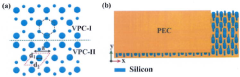
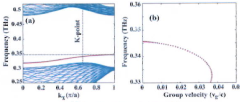
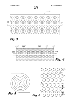
A topological waveguide device and its method for dispersionless slow light transmission at terahertz (THZ) frequencies
PatentInactiveIN202141033040A
Innovation
- A topological waveguide device utilizing a valley photonic crystal structure with dielectric rods in a honeycomb lattice, leveraging the Valley Hall effect to achieve robust and dispersionless slow light propagation, protected by topological edge states.
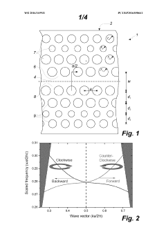
A slow-light generating optical device and a method of producing slow light with low losses
PatentWO2016169931A1
Innovation
- A slow-light generating optical device with a planar waveguide designed to have glide-plane symmetric nanostructures on either side, ensuring that forward and backward propagating modes are individually non-degenerate but mutually degenerate, thereby minimizing backscattering and allowing for extended delay lines with low losses.


Materials Science Considerations for Device Fabrication
The fabrication of slow-light devices based on topological photonics requires careful consideration of material properties and processing techniques. Silicon-based platforms remain dominant due to their compatibility with existing semiconductor manufacturing processes, offering precise control over nanoscale features essential for topological photonic structures. However, the inherent material loss in silicon at optical frequencies presents a significant challenge for slow-light applications where signal preservation is critical.
Alternative materials such as silicon nitride (Si3N4) and aluminum nitride (AlN) have emerged as promising candidates due to their lower optical losses and wider bandgaps. These materials enable operation across broader wavelength ranges while maintaining high refractive index contrast necessary for strong light confinement. For quantum applications of slow-light devices, III-V semiconductors like gallium arsenide (GaAs) and indium phosphide (InP) offer direct bandgaps that facilitate integration with quantum emitters.
The fabrication of topological photonic structures demands nanometer-scale precision to maintain the delicate balance of symmetries that enable topological protection. Electron beam lithography remains the gold standard for prototype development, though its throughput limitations present challenges for mass production. Advanced techniques such as nanoimprint lithography and self-assembly methods are being explored to overcome these scaling barriers.
Material interfaces in multilayer structures require particular attention, as interface roughness can introduce scattering that disrupts topological protection mechanisms. Atomic layer deposition (ALD) has proven valuable for creating ultra-smooth interfaces with atomic-level control. Additionally, stress management becomes crucial when combining materials with different thermal expansion coefficients, as strain can alter the band structure and potentially destroy topological features.
Temperature stability represents another critical consideration, particularly for applications requiring cryogenic operation such as quantum information processing. Materials must maintain their optical and mechanical properties across wide temperature ranges without introducing additional loss mechanisms or structural deformations that could compromise topological protection.
Post-fabrication tuning capabilities through electro-optic, thermo-optic, or mechanical means provide valuable flexibility for optimizing device performance. Materials with strong electro-optic coefficients like lithium niobate (LiNbO3) enable dynamic control of slow-light properties, though integration challenges with standard photonic platforms must be addressed through techniques such as thin-film bonding or heterogeneous integration.
Integration Pathways with Existing Photonic Platforms
The integration of slow-light devices based on topological photonics with existing photonic platforms represents a critical challenge and opportunity for practical applications. Current silicon photonics, III-V semiconductor platforms, and integrated optical circuits provide established manufacturing ecosystems that any new technology must leverage to achieve commercial viability.
Silicon photonics offers the most promising immediate integration pathway due to its mature fabrication processes and compatibility with CMOS technology. Researchers have demonstrated successful implementation of topological photonic structures on silicon-on-insulator (SOI) platforms, enabling slow-light waveguides that can be directly incorporated into existing photonic integrated circuits (PICs). The primary challenge lies in maintaining topological protection while interfacing with conventional waveguide structures.
For III-V semiconductor platforms, integration efforts focus on creating active-passive interfaces between topological slow-light regions and conventional gain media. Recent experimental work has shown promising results in GaAs/AlGaAs systems where topological edge states can be coupled with quantum wells to create novel light-emitting devices with controlled group velocity. These hybrid approaches leverage the superior light emission properties of III-V materials while exploiting topological protection for slow-light propagation.
Planar lightwave circuit (PLC) technologies based on silica and polymer waveguides present another integration avenue. The relatively large feature sizes in these platforms simplify fabrication of complex topological lattice structures, though the weak index contrast limits the strength of topological effects. Researchers have addressed this limitation by incorporating high-index nanoparticles or resonant structures to enhance light-matter interactions while maintaining compatibility with PLC manufacturing processes.
Vertical integration strategies are emerging as particularly promising, where topological photonic layers are bonded or grown on conventional photonic platforms. This approach allows separate optimization of the slow-light functionality and the underlying photonic circuitry. Recent demonstrations include topological photonic crystal membranes bonded to silicon waveguide circuits, enabling efficient coupling between slow-light modes and conventional photonic components.
Standardization efforts are underway to develop design rules and process development kits (PDKs) that incorporate topological photonic elements into established foundry services. These initiatives aim to lower the barrier to adoption by providing designers with verified building blocks that leverage slow-light effects while maintaining compatibility with existing photonic design workflows and manufacturing capabilities.
Unlock deeper insights with Patsnap Eureka Quick Research — get a full tech report to explore trends and direct your research. Try now!
Generate Your Research Report Instantly with AI Agent
Supercharge your innovation with Patsnap Eureka AI Agent Platform!