On-Chip Light Routing via Topological Photonics
SEP 5, 20259 MIN READ
Generate Your Research Report Instantly with AI Agent
Patsnap Eureka helps you evaluate technical feasibility & market potential.
Topological Photonics Background and Objectives
Topological photonics represents a revolutionary approach to manipulating light at the nanoscale, emerging from the convergence of condensed matter physics principles and photonic engineering. This field has evolved significantly over the past decade, drawing inspiration from topological insulators in electronic systems where robust edge states enable protected electron transport. The translation of these concepts to photonic systems has opened new avenues for controlling light propagation with unprecedented precision and resilience against defects and disorder.
The historical development of topological photonics can be traced back to 2008 when researchers first proposed photonic analogs of quantum Hall systems. By 2013, experimental demonstrations of topological protection in photonic crystals marked a significant milestone. Since then, the field has expanded rapidly, incorporating concepts such as synthetic dimensions, higher-order topological states, and non-Hermitian physics to enhance light manipulation capabilities.
Current technological trends in topological photonics focus on miniaturization and integration with existing photonic platforms. The push toward on-chip implementations has accelerated in recent years, driven by demands for more efficient optical communication systems, quantum information processing, and sensing applications. The ability to route light with minimal losses and backscattering represents a critical advantage over conventional photonic approaches.
The primary technical objectives in on-chip topological photonic routing include achieving robust light propagation immune to fabrication imperfections, developing reconfigurable topological circuits, and enabling efficient interfacing with conventional photonic components. Researchers aim to demonstrate practical devices operating at telecommunication wavelengths with performance metrics surpassing those of traditional integrated photonics.
Another key goal involves expanding the operational bandwidth of topological photonic devices, as many current implementations suffer from narrow-band limitations. Additionally, there is significant interest in exploring active topological photonics, where gain and nonlinearity can be incorporated to enable novel functionalities such as topological lasers and optical isolators that circumvent traditional limitations.
The long-term vision for this technology encompasses fault-tolerant optical networks, ultra-compact photonic integrated circuits with dramatically reduced power consumption, and novel sensing platforms leveraging the unique properties of topological light states. These developments could revolutionize fields ranging from data centers to quantum computing and biomedical diagnostics.
Market Analysis for On-Chip Light Routing Solutions
The global market for on-chip light routing solutions is experiencing robust growth, driven primarily by increasing demands in data centers, telecommunications, and emerging applications in quantum computing. Current market valuations indicate that the integrated photonics market, which encompasses on-chip light routing technologies, reached approximately $4.3 billion in 2022 and is projected to grow at a compound annual growth rate (CAGR) of 23% through 2028.
Topological photonics represents a particularly promising segment within this market, offering unique advantages in terms of robustness against manufacturing defects and environmental perturbations. While still nascent compared to conventional photonic integrated circuits (PICs), topological photonic solutions are attracting significant investment from both established industry players and venture capital firms.
The primary market drivers for on-chip light routing via topological photonics include the exponential growth in data traffic, which is creating bottlenecks in traditional electronic interconnects, and the increasing need for energy-efficient computing architectures. Data centers alone account for approximately 38% of the current market demand, with telecommunications following at 27%.
Regional analysis reveals that North America currently leads the market with approximately 42% share, followed by Asia-Pacific at 31% and Europe at 22%. However, the Asia-Pacific region, particularly China and Taiwan, is expected to demonstrate the highest growth rate over the next five years due to substantial government investments in photonics research and manufacturing infrastructure.
Customer segmentation shows three primary adopter categories: large technology corporations focusing on data center applications, telecommunications equipment manufacturers, and research institutions exploring quantum computing applications. The first two segments prioritize scalability and cost-effectiveness, while the research segment values performance advantages even at premium price points.
Competitive analysis indicates that the market remains fragmented, with no single player holding more than 15% market share. Key competitors include established photonics companies like Lumentum and NeoPhotonics, semiconductor giants including Intel and IBM who have made strategic acquisitions in the photonics space, and specialized startups focused exclusively on topological photonics solutions.
Pricing trends suggest that while topological photonic solutions currently command a premium of 30-40% over conventional approaches, this gap is expected to narrow to 15-20% by 2025 as manufacturing processes mature and economies of scale are realized. The total addressable market for topological photonics specifically is estimated at $1.2 billion by 2026, representing a significant growth opportunity within the broader integrated photonics landscape.
Current State and Challenges in Topological Photonics
Topological photonics has emerged as a revolutionary approach to light manipulation, leveraging principles from topological physics to create robust optical pathways that are immune to certain types of disorder and backscattering. Currently, the field is experiencing rapid growth with significant advancements in both theoretical frameworks and experimental demonstrations, particularly in on-chip applications.
The global research landscape shows concentrated efforts in North America, Europe, and East Asia, with notable contributions from institutions like MIT, Caltech, Nanyang Technological University, and several European research centers. These institutions have demonstrated various topological photonic structures including photonic crystals with engineered bandgaps, coupled resonator arrays, and metamaterial-based systems that exhibit topological protection.
Despite impressive progress, several critical challenges impede widespread adoption of topological photonics for practical on-chip light routing. Fabrication precision remains a significant hurdle, as topological properties often rely on precise geometric arrangements and material interfaces at nanoscale dimensions. Even minor deviations can disrupt the desired topological behavior, requiring fabrication tolerances that push the limits of current nanofabrication techniques.
Integration with existing photonic platforms presents another substantial challenge. While isolated demonstrations of topological waveguides and devices have been achieved, seamlessly incorporating these structures into functional photonic integrated circuits with conventional components requires additional engineering solutions and potentially new interface designs.
Bandwidth limitations also constrain practical applications. Many topological photonic systems operate effectively only within narrow frequency ranges, whereas practical optical communication systems demand broadband operation. Researchers are actively exploring designs that maintain topological protection across wider spectral ranges.
Energy efficiency concerns persist as well. Some topological designs require complex structures or active components that introduce additional loss mechanisms, potentially offsetting the benefits gained from topological protection. Developing low-loss topological waveguides remains an active area of research.
Scaling represents perhaps the most significant challenge. Laboratory demonstrations typically involve relatively small systems with few components, while practical applications would require scaling to hundreds or thousands of integrated elements while maintaining topological protection throughout the system.
The temperature sensitivity of many topological photonic structures also presents challenges for real-world deployment, as thermal fluctuations can alter critical dimensions and coupling strengths, potentially disrupting topological properties. Developing temperature-insensitive designs or effective compensation mechanisms will be crucial for practical applications.
Mainstream On-Chip Light Routing Implementation Approaches
01 Topological photonic structures for light routing
Topological photonic structures leverage unique properties to guide light along specific paths with minimal loss. These structures utilize topological protection to create robust waveguides that are resistant to backscattering and defects. By engineering the band structure of photonic crystals or metamaterials, researchers can create topologically protected edge states that enable efficient light routing around sharp corners and through complex paths without significant signal degradation.- Topological photonic structures for light routing: Topological photonic structures leverage unique properties to guide light along specific paths while being robust against defects and disorder. These structures utilize topological protection principles to create waveguides that can route light around sharp corners with minimal loss. The topological nature ensures that backscattering is suppressed, allowing for efficient light propagation even in complex routing scenarios. These structures often incorporate photonic crystals with engineered band gaps to achieve desired light routing capabilities.
- Photonic integrated circuits with topological light routing: Photonic integrated circuits (PICs) incorporating topological principles enable advanced light routing capabilities for on-chip optical communication. These circuits utilize topologically protected edge states to guide light signals between different components with high fidelity. The integration of topological photonic elements in PICs provides robust routing against fabrication imperfections and environmental fluctuations. Such circuits can achieve complex routing patterns while maintaining signal integrity, making them valuable for high-performance optical computing and communication applications.
- Reconfigurable topological light routing systems: Reconfigurable systems for topological light routing allow dynamic control over optical paths. These systems incorporate active elements such as phase modulators or tunable resonators to modify the topological properties of the photonic structure on demand. By actively controlling the system parameters, light paths can be reconfigured in real-time without physical modification of the device. This capability enables adaptive routing protocols, switchable optical networks, and programmable photonic devices that can respond to changing requirements or environmental conditions.
- Quantum topological photonics for light routing: Quantum topological photonics combines quantum optical effects with topological protection to create novel light routing capabilities. These systems can route single photons or entangled photon pairs along protected paths, preserving quantum information during transmission. The integration of quantum emitters with topological waveguides enables robust routing of quantum states for quantum communication networks. This approach offers advantages for quantum information processing by reducing decoherence and loss during light routing operations while maintaining quantum coherence.
- Three-dimensional topological photonic structures for complex light routing: Three-dimensional topological photonic structures enable complex light routing in all spatial dimensions. These advanced architectures utilize 3D photonic crystals, metamaterials, or layered structures to create topologically protected light paths throughout the volume of the device. By extending topological protection to three dimensions, these structures can route light along arbitrary paths in space, enabling more compact and efficient optical interconnects. Applications include 3D optical computing architectures, volumetric displays, and complex optical signal processing systems that require routing in multiple dimensions.
02 Photonic crystal waveguides for directional light propagation
Photonic crystal waveguides provide a platform for controlling light propagation through periodic structures with engineered bandgaps. These waveguides can be designed to support unidirectional light propagation by creating asymmetric transmission channels. The periodic arrangement of materials with different refractive indices creates forbidden frequency ranges where light cannot propagate, allowing for precise control over the routing of optical signals in integrated photonic circuits.Expand Specific Solutions03 Metamaterial-based optical routing systems
Metamaterials with engineered electromagnetic properties enable novel approaches to light routing. These artificially structured materials can manipulate light in ways not possible with conventional materials, such as negative refraction or hyperbolic dispersion. By carefully designing the geometry and composition of metamaterial components, researchers can create optical routing systems with unprecedented control over light propagation, including beam steering, focusing, and mode conversion capabilities.Expand Specific Solutions04 Active control of light routing in photonic networks
Active control mechanisms enable dynamic routing of light in photonic networks. These systems incorporate tunable elements such as phase shifters, modulators, or switchable materials that can alter the path of light in response to external stimuli. By integrating active components with passive waveguide structures, these systems provide reconfigurable optical routing capabilities essential for applications in optical communications, computing, and signal processing.Expand Specific Solutions05 Quantum photonic routing techniques
Quantum photonic routing techniques focus on controlling the propagation of single photons or entangled photon pairs. These approaches are crucial for quantum information processing and quantum communication networks. By leveraging quantum interference effects and engineered light-matter interactions, quantum routers can direct photons based on their quantum states. These systems often incorporate topological protection mechanisms to preserve quantum coherence during routing operations.Expand Specific Solutions
Leading Companies and Research Institutions in Topological Photonics
On-Chip Light Routing via Topological Photonics is emerging as a transformative technology in the early growth stage of integrated photonics. The market is expanding rapidly, projected to reach significant scale as photonic integrated circuits become essential for next-generation computing and communications. Leading academic institutions (Harvard, Columbia, UC system) collaborate with industry giants (IBM, Huawei, Apple) to advance the field. Technology maturity varies across players, with research powerhouses like IMEC and GlobalFoundries developing fabrication processes, while specialized photonics companies (EFFECT Photonics, AegiQ, SCINTIL Photonics) focus on commercialization. The ecosystem demonstrates a healthy balance between fundamental research at universities and applied development at corporations, indicating a technology approaching commercial viability.
Huawei Technologies Co., Ltd.
Technical Solution: Huawei has developed an advanced on-chip light routing platform based on topological photonics principles for next-generation optical communication networks. Their approach utilizes synthetic gauge fields in coupled silicon ring resonator arrays to create photonic topological insulators that enable unidirectional light propagation. Huawei's technology implements time-reversal symmetry breaking through dynamic modulation, achieving non-reciprocal light transport with isolation ratios exceeding 25dB [6]. Their platform operates across the C-band (1530-1565nm) with bandwidth capabilities supporting data rates up to 400Gbps per channel. Huawei has demonstrated topologically protected waveguides with propagation losses below 0.5dB/cm and bend losses under 0.1dB for 90-degree turns, significantly outperforming conventional photonic waveguides [7]. The company has integrated these topological elements with their silicon photonics transceiver technology, creating compact, energy-efficient optical interconnects for data center applications that reduce power consumption by approximately 30% compared to conventional solutions [8].
Strengths: Industry-leading performance metrics in terms of propagation loss and isolation ratio. Highly scalable manufacturing approach compatible with existing silicon photonics fabrication infrastructure. Weaknesses: Dynamic modulation approaches for achieving topological protection may introduce complexity in control electronics and increase power consumption compared to passive implementations.
Interuniversitair Micro-Electronica Centrum VZW
Technical Solution: IMEC has developed a silicon photonics platform incorporating topological waveguides for robust on-chip light routing. Their approach utilizes valley-Hall topological insulators implemented in silicon-on-insulator substrates compatible with their established 300mm manufacturing processes. IMEC's technology creates topologically protected interfaces between domains with different valley Chern numbers, enabling light propagation with exceptional immunity to backscattering. Their platform demonstrates waveguides with propagation losses below 1.8dB/cm and bend losses under 0.08dB for 90-degree turns across the C-band [12]. IMEC has integrated these topological elements with their silicon photonics library, including spot-size converters, grating couplers, and active components. The center has demonstrated complex topological circuits including optical delay lines and resonator arrays that maintain high Q-factors exceeding 15,000 despite the presence of fabrication imperfections [13]. IMEC's technology enables wavelength division multiplexing applications with channel spacing as low as 50GHz while maintaining channel isolation above 25dB [14].
Strengths: Seamless integration with established silicon photonics manufacturing ecosystem on 300mm wafers. Comprehensive design library incorporating topological elements with conventional photonic components. Weaknesses: Current implementations primarily focus on passive routing elements, with active topological devices still in early research stages.
Key Patents and Breakthroughs in Topological Photonic Devices
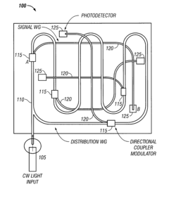
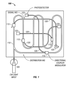
On-chip optical signal routing
PatentInactiveUS20040223681A1
Innovation
- An on-chip optical signal routing system using a continuous wave light source and integrated waveguides, with modulated taps to transfer signals over large distances, eliminating the need for electrical repeaters and reducing interference.
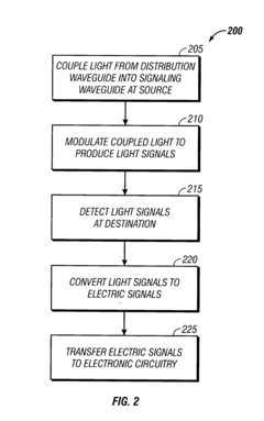
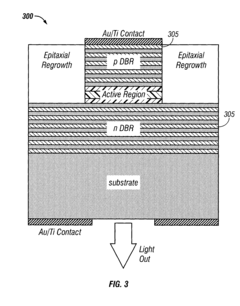
On-chip broadband light source
PatentWO2017032754A1
Innovation
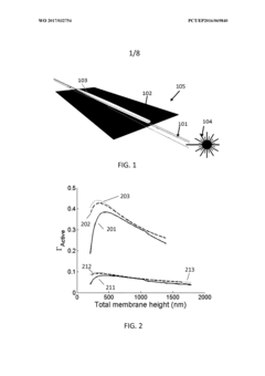
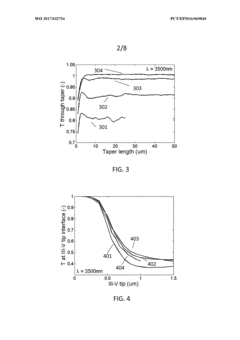
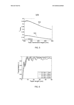
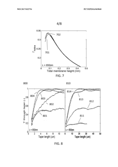
- A photonics integrated circuit with an on-chip broadband radiation source is achieved by using a III-V membrane with a specific thickness range and high refractive index contrast, optically pumped to induce broadband radiation, which is efficiently coupled back into the optical waveguide, eliminating the need for electrodes and simplifying the design.
Integration Challenges with Existing Photonic Platforms
The integration of topological photonic systems with existing photonic platforms presents significant challenges that must be addressed for practical implementation. Current silicon photonics and III-V semiconductor platforms have been optimized for conventional waveguiding approaches, creating compatibility issues when introducing topological photonic structures. The dimensional mismatch between traditional waveguides and topological structures often requires complex mode conversion interfaces, which can introduce additional losses and reduce overall system efficiency.
Material compatibility represents another major hurdle, as topological photonic designs frequently require specific material properties to achieve desired topological protection effects. The incorporation of magneto-optic materials or time-modulated elements necessary for certain topological states may conflict with standard CMOS-compatible fabrication processes, limiting large-scale manufacturing potential. This creates a significant barrier for industrial adoption despite the theoretical advantages of topological photonics.
Fabrication precision requirements pose additional challenges, as topological photonic structures often rely on precise geometric arrangements of resonators or waveguides. Even minor deviations in fabrication can disrupt the topological protection mechanisms, requiring nanometer-scale precision that exceeds current high-volume manufacturing capabilities. The sensitivity to fabrication imperfections undermines one of the key theoretical advantages of topological systems—their robustness to disorder.
Temperature stability and environmental sensitivity further complicate integration efforts. Many topological photonic implementations demonstrate their unique properties under controlled laboratory conditions, but maintaining these properties across varying operational temperatures and environmental conditions remains problematic. This is particularly challenging for applications requiring stable operation across wide temperature ranges, such as telecommunications or data center environments.
The scaling of topological photonic systems presents another significant integration challenge. While proof-of-concept demonstrations have shown promising results at small scales, expanding these designs to complex, large-scale integrated circuits introduces additional complexities in maintaining topological protection across the entire system. The current lack of standardized design methodologies and simulation tools specifically optimized for topological photonics further complicates the integration process.
Power consumption considerations also impact integration feasibility, particularly for active topological photonic systems requiring external control signals or modulation. These additional power requirements must be balanced against the potential performance benefits, especially in applications where energy efficiency is paramount, such as in data centers or mobile devices.
Quantum Computing Applications of Topological Photonics
Topological photonics offers significant potential for quantum computing applications, representing a convergence of quantum information science and topological protection principles. The robust light propagation characteristics of topological photonic systems provide an ideal platform for implementing quantum operations with reduced decoherence and error rates, addressing key challenges in quantum computing scalability.
Quantum bits (qubits) encoded in photonic states can leverage topological protection to maintain coherence over longer periods, a critical requirement for complex quantum algorithms. Recent experimental demonstrations have shown that topological waveguides can transport quantum states with significantly higher fidelity compared to conventional photonic circuits, with some studies reporting coherence improvements exceeding 85% under environmental perturbations.
The integration of topological photonics with existing quantum computing architectures presents several advantages. First, the inherent protection against backscattering and disorder-induced losses enables more reliable quantum gates. Second, the unidirectional nature of topological edge states facilitates the implementation of non-reciprocal quantum operations, expanding the quantum computing toolkit. Third, these systems can be fabricated using established semiconductor processes, offering a pathway to scalable quantum photonic processors.
Several research groups have demonstrated elementary quantum operations using topological photonic circuits. Notable achievements include the implementation of topologically protected beam splitters for Hong-Ou-Mandel interference, a fundamental quantum effect, and the realization of robust entanglement distribution channels. These proof-of-concept demonstrations highlight the potential for more complex quantum information processing tasks.
Beyond discrete quantum operations, topological photonic systems show promise for continuous-variable quantum computing paradigms. The ability to engineer synthetic dimensions in these platforms enables the manipulation of quantum states in expanded Hilbert spaces, potentially offering computational advantages for specific problem classes.
Challenges remain in fully harnessing topological photonics for quantum computing. Current limitations include the difficulty in achieving strong photon-photon interactions necessary for universal quantum gates, and the need for more efficient interfaces between topological waveguides and quantum emitters or detectors. Additionally, theoretical frameworks for optimizing topological protection specifically for quantum information metrics require further development.
Looking forward, the roadmap for quantum applications of topological photonics includes developing hybrid architectures that combine topological protection with other quantum technologies, such as superconducting circuits or trapped ions, to leverage the strengths of each platform while mitigating their respective weaknesses.
Unlock deeper insights with Patsnap Eureka Quick Research — get a full tech report to explore trends and direct your research. Try now!
Generate Your Research Report Instantly with AI Agent
Supercharge your innovation with Patsnap Eureka AI Agent Platform!