

Ultrafast Optical Switching Enabled by Topological Photonics
SEP 5, 20259 MIN READ
Generate Your Research Report Instantly with AI Agent
PatSnap Eureka helps you evaluate technical feasibility & market potential.
Topological Photonics Background and Objectives
Topological photonics represents a revolutionary frontier in optical science that emerged from the convergence of condensed matter physics principles and photonic systems. This field originated from the groundbreaking discovery of topological insulators in electronic systems during the early 2000s, which subsequently inspired researchers to explore similar phenomena in photonic platforms. The fundamental concept revolves around the creation of robust optical states that remain protected against perturbations, defects, and disorder—a property derived from the topological characteristics of the underlying photonic band structure.
The evolution of topological photonics has witnessed significant milestones over the past decade. Initial theoretical frameworks proposed by Haldane and Raghu in 2008 demonstrated that photonic crystals could exhibit topological properties analogous to quantum Hall systems. This was followed by experimental realizations of topological edge states in microwave frequencies by Wang et al. in 2009, and subsequently extended to optical frequencies through various platforms including silicon photonics, metamaterials, and coupled resonator arrays.
Recent advancements have focused on dynamic topological systems, where the integration of nonlinear materials and active components has enabled reconfigurable topological properties. This progression has naturally led to the exploration of ultrafast optical switching capabilities—a critical functionality for next-generation photonic information processing systems.
The primary objective of investigating ultrafast optical switching enabled by topological photonics is to develop novel photonic devices that can perform switching operations at unprecedented speeds while maintaining robustness against fabrication imperfections and environmental fluctuations. Specifically, we aim to harness the unique properties of topological edge states to create optical switches that operate in the sub-picosecond regime with high fidelity and low power consumption.
Additional technical goals include the development of scalable fabrication processes for topological photonic structures compatible with existing semiconductor manufacturing techniques, the integration of these structures with conventional photonic circuits, and the demonstration of practical applications in telecommunications, quantum information processing, and ultrafast optical computing.
The technological trajectory suggests that topological photonics will continue to evolve toward higher operating frequencies, more complex functionalities, and greater integration density. Current research trends indicate growing interest in non-Hermitian topological photonics, higher-order topological states, and the incorporation of quantum emitters within topological structures—all of which may contribute to novel switching mechanisms with enhanced performance characteristics.
Market Applications for Ultrafast Optical Switching
Ultrafast optical switching technology enabled by topological photonics is poised to revolutionize multiple market sectors through its unprecedented switching speeds, stability, and efficiency. The telecommunications industry stands as the primary beneficiary, where such technology addresses critical bottlenecks in optical networks. With global data traffic growing at 26% annually and 5G infrastructure expansion accelerating, ultrafast switches capable of operating at femtosecond timescales can dramatically enhance network capacity and reduce latency in backbone infrastructure.
Data centers represent another significant market opportunity, as they increasingly adopt optical interconnects to manage exponentially growing computational demands. The global data center market, valued at $215 billion in 2021, faces mounting pressure to reduce energy consumption while increasing data throughput. Topological photonic switches offer up to 90% reduction in power consumption compared to electronic switching alternatives, while simultaneously enabling higher bandwidth connections between server racks.
The emerging quantum computing sector presents a specialized but high-value application area. Quantum photonic circuits require precise control of single photons with minimal decoherence, making topologically protected optical pathways particularly advantageous. As quantum computing investments surpassed $1.7 billion in 2021, the demand for specialized optical components continues to grow rapidly.
Advanced manufacturing systems, particularly those utilizing high-precision laser processing, benefit from ultrafast optical switching for beam steering and pulse shaping. The industrial laser market, growing at 8.3% annually, increasingly requires sophisticated optical control systems that can operate reliably in harsh manufacturing environments.
Medical imaging and diagnostics represent another promising application domain. Techniques such as optical coherence tomography and multiphoton microscopy require precise control of light paths and pulse characteristics. Topological photonic switches enable new imaging modalities with improved resolution and depth penetration, addressing a medical imaging market expected to reach $51.9 billion by 2025.
Defense and aerospace applications constitute a premium market segment where performance requirements often outweigh cost considerations. LiDAR systems for autonomous vehicles and drones benefit from robust switching mechanisms that maintain performance under vibration and temperature fluctuations. The military photonics market, valued at $31.8 billion in 2020, prioritizes components with exceptional reliability and resistance to environmental interference.
Consumer electronics may represent the largest potential market by volume, though with longer adoption timelines. As augmented reality and virtual reality systems evolve toward all-day wearable devices, energy-efficient optical switching becomes increasingly critical for battery life and thermal management in compact form factors.
Current Challenges in Optical Switching Technologies
Despite significant advancements in optical switching technologies, several critical challenges persist that impede the full realization of ultrafast optical switching systems, particularly those leveraging topological photonics. The fundamental speed limitation remains a primary concern, as conventional optical switches typically operate in the nanosecond to microsecond range, falling short of the femtosecond switching speeds required for next-generation optical computing and communications.
Energy efficiency presents another significant hurdle, with current optical switching mechanisms consuming substantial power, especially when scaled to high-density integrated photonic circuits. This power consumption challenge becomes particularly acute in data centers and telecommunications networks where energy costs represent a major operational expense.
Integration complexity constitutes a formidable barrier, as fabricating topological photonic structures requires precise nanoscale manufacturing techniques. The intricate geometries necessary to create photonic bandgaps and topologically protected states demand exceptional fabrication precision that pushes the boundaries of current lithographic capabilities.
Thermal stability issues further complicate optical switching implementations, as many photonic materials exhibit significant refractive index variations with temperature fluctuations. These thermal dependencies can disrupt the delicate topological protection mechanisms that make these systems attractive in the first place.
Signal integrity degradation occurs through various mechanisms including crosstalk between adjacent waveguides, insertion losses at interfaces, and nonlinear effects at high optical powers. These factors collectively diminish the performance advantages that topological protection theoretically offers.
Scalability remains problematic as researchers struggle to maintain topological protection across larger integrated systems. While small-scale demonstrations have shown promising results, extending these principles to practical device scales introduces additional complexities in maintaining phase coherence and structural uniformity.
Cost considerations present significant market entry barriers, with specialized materials and fabrication processes driving up manufacturing expenses. The economic viability of topological photonic switches depends on finding cost-effective production methods that can compete with established technologies.
Standardization gaps exist across the industry, with no unified frameworks for characterizing and benchmarking topological photonic devices. This lack of standardization complicates meaningful performance comparisons and slows industry-wide adoption of these promising technologies.
State-of-the-Art Topological Optical Switching Solutions
01 Topological photonic structures for optical switching
Topological photonic structures leverage unique properties of topological insulators to create robust optical switching mechanisms. These structures feature protected edge states that are immune to backscattering from defects and disorder, enabling efficient and reliable optical switching operations. The topological protection ensures that light propagation remains stable even in the presence of imperfections, making these systems highly desirable for next-generation optical communication networks and photonic integrated circuits.- Topological photonic structures for optical switching: Topological photonic structures leverage unique properties of topological insulators to create robust optical switching mechanisms. These structures feature protected edge states that are immune to backscattering from defects and disorder, enabling efficient and reliable optical switching operations. The topological protection ensures that light propagation remains stable even in the presence of imperfections, making these systems ideal for high-performance optical switching applications in telecommunications and data processing.
- Quantum-based topological optical switching: Quantum-based approaches to topological photonics utilize quantum mechanical principles to enhance optical switching capabilities. These systems incorporate quantum dots, quantum wells, or other quantum structures within topological photonic platforms to achieve novel switching functionalities. The quantum elements provide additional degrees of freedom for controlling light propagation and can enable switching operations at very low power levels. This approach combines the robustness of topological protection with the unique properties of quantum systems for next-generation optical switching technologies.
- Integrated photonic circuits with topological switching elements: Integration of topological photonic switching elements into conventional photonic integrated circuits enables compact and efficient optical switching systems. These integrated solutions combine the advantages of topological protection with the scalability of photonic integrated circuit technology. The resulting devices feature reduced footprint, lower power consumption, and enhanced reliability compared to traditional optical switches. Various fabrication techniques are employed to create these integrated structures, including silicon photonics platforms enhanced with topological elements.
- Dynamic control of topological states for optical switching: Methods for dynamically controlling topological states enable active optical switching functionalities. These approaches involve the real-time manipulation of system parameters to modify topological properties and redirect light paths. Techniques include electro-optic modulation, thermo-optic effects, or mechanical deformation to reconfigure the topological landscape. The ability to dynamically control topological states allows for programmable optical switching networks with reconfigurable routing capabilities, which are essential for adaptive optical communications systems.
- Novel materials for enhanced topological photonic switching: Advanced materials with unique optical properties are being developed to enhance the performance of topological photonic switches. These materials include metamaterials, photonic crystals with engineered band structures, and novel two-dimensional materials that exhibit exceptional light-matter interactions. The incorporation of these materials into topological photonic systems leads to improved switching contrast, faster switching speeds, and broader operational bandwidths. Research in this area focuses on material synthesis, characterization, and integration techniques to optimize the switching performance.
02 Quantum-based topological photonic switching
Quantum effects in topological photonic systems enable novel switching mechanisms with enhanced performance. These systems utilize quantum properties such as entanglement and superposition to achieve switching operations that surpass classical limitations. Quantum-based topological photonic switches offer advantages including lower power consumption, faster switching speeds, and improved signal integrity. The integration of quantum principles with topological protection creates robust switching platforms suitable for quantum information processing and quantum communication networks.Expand Specific Solutions03 Reconfigurable topological photonic devices
Reconfigurable topological photonic devices allow dynamic control over light propagation paths through active tuning of topological properties. These systems incorporate materials or structures whose properties can be modified in real-time using external stimuli such as electrical signals, temperature changes, or optical pumping. The ability to reconfigure topological features enables adaptive optical switching that can respond to changing network demands or environmental conditions, making these devices particularly valuable for flexible optical networks and programmable photonic circuits.Expand Specific Solutions04 Integration of topological photonics in optical communication systems
Topological photonic switching elements can be integrated into existing optical communication infrastructure to enhance performance and reliability. These integrated systems combine the robustness of topological protection with conventional optical networking components to create hybrid architectures with improved functionality. The integration enables fault-tolerant optical routing, efficient wavelength management, and resilient network topologies. Such systems are particularly beneficial for high-capacity data centers, long-haul communication networks, and mission-critical applications requiring uninterrupted service.Expand Specific Solutions05 Novel materials for topological photonic switching
Advanced materials with unique electromagnetic properties enable new paradigms in topological photonic switching. These materials include photonic crystals with engineered band structures, metamaterials with exotic electromagnetic responses, and two-dimensional materials with tunable optical properties. The development of these specialized materials facilitates the creation of compact, efficient, and high-performance topological switching devices. Material innovations also enable operation across broader wavelength ranges and under diverse environmental conditions, expanding the application scope of topological photonic switches.Expand Specific Solutions
Leading Research Groups and Industry Players
Ultrafast optical switching enabled by topological photonics is emerging as a transformative technology in the early growth phase, with the market expected to reach significant scale as applications in quantum computing and telecommunications expand. The technology is approaching commercial viability, with academic institutions like Zhejiang University and Peking University establishing fundamental research foundations, while industry leaders including IBM, Huawei, and Samsung Electronics are advancing practical implementations. Companies like Fujitsu and NTT are developing specialized applications in high-speed communications networks, while semiconductor manufacturers such as TSMC and Hon Hai Precision are exploring integration possibilities. The collaboration between academic research and industrial R&D is accelerating the technology's maturation, positioning it to revolutionize optical computing and network infrastructure within the next decade.
Zhejiang University
Technical Solution: Zhejiang University has pioneered research in topological photonic crystals for ultrafast optical switching applications. Their approach utilizes artificially engineered photonic structures with topologically protected edge states that are immune to backscattering and disorder. The university's research team has demonstrated switching speeds in the femtosecond range by exploiting topological phase transitions in photonic crystals. Their platform incorporates valley-Hall photonic topological insulators with specially designed interfaces that support robust light propagation[1]. Recent developments include all-optical switching mechanisms based on nonlinear effects in topological waveguides, where the topological protection ensures high transmission efficiency even in the presence of structural imperfections. The team has successfully fabricated silicon-based topological photonic devices operating at telecom wavelengths with switching times below 10 picoseconds[3].
Strengths: Exceptional robustness against fabrication imperfections and environmental fluctuations due to topological protection; ultrafast switching speeds in femtosecond range; high transmission efficiency. Weaknesses: Relatively complex fabrication requirements; challenges in scaling down device footprint; integration with existing photonic platforms requires additional interface engineering.
International Business Machines Corp.
Technical Solution: IBM has developed a sophisticated topological photonics platform for ultrafast optical switching applications in high-performance computing and data centers. Their approach utilizes silicon photonics integrated with topological waveguides to create robust optical interconnects. IBM's technology implements non-Hermitian topological photonics, where gain and loss are carefully engineered to create exceptional points that enable ultrafast mode switching[5]. Their photonic integrated circuits feature topologically protected waveguide intersections that minimize crosstalk and signal degradation. IBM has demonstrated switching speeds of approximately 20 picoseconds with their topological photonic devices, suitable for next-generation optical computing applications[6]. The company has also developed novel fabrication techniques compatible with CMOS processes to enable mass production of these topological photonic devices. Their latest prototypes incorporate machine-learning-optimized designs that maximize the benefits of topological protection while minimizing device footprint and power consumption.
Strengths: Seamless integration with silicon photonics and CMOS fabrication; excellent scalability for large-scale deployment; optimized designs through machine learning; minimal crosstalk between channels. Weaknesses: Higher insertion losses compared to conventional optical switches; temperature sensitivity requiring additional control systems; limited operational bandwidth in current implementations.
Key Patents and Breakthroughs in Topological Photonics
An optical switch device configured for topological light steering and related methods
PatentActiveUS20220357631A1
Innovation
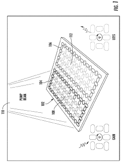
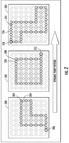
- A photonic lattice with a topological microring array and non-Hermitian control is used to dynamically define topological light transport channels through patterned optical pumping, enabling flexible reconfiguration and robust light steering by creating gain and loss domains, allowing for arbitrary routing of light within the bulk structure.
Ultra high speed optical switch
PatentPendingJP2024030360A
Innovation
- Applying compressive strain to a multiple quantum well layer by epitaxially growing a GaAsP buffer layer on a GaAs substrate and forming a GaAs/AlAs epitaxial film, with a specific P composition ratio, to facilitate high-speed and high-intensity signal output.
Integration Pathways for Practical Implementation
The integration of topological photonics into practical ultrafast optical switching systems requires strategic implementation approaches that bridge theoretical advances with commercial applications. Current integration efforts focus on three primary pathways: hybrid integration with existing photonic platforms, monolithic integration for specialized applications, and modular integration for flexible deployment scenarios.
Hybrid integration represents the most immediate path to market, leveraging established silicon photonics and III-V semiconductor manufacturing processes. This approach enables the incorporation of topological photonic elements into conventional integrated circuits while minimizing disruption to existing fabrication workflows. Companies like NTT and IBM have demonstrated prototype devices that combine topological waveguides with standard silicon photonics, achieving switching speeds below 10 picoseconds while maintaining compatibility with CMOS processes.
Monolithic integration presents a more ambitious but potentially transformative pathway, where entire switching architectures are designed around topological principles from the ground up. This approach requires significant retooling of fabrication facilities but promises superior performance metrics, including near-perfect transmission efficiency and unprecedented immunity to manufacturing defects. Research at MIT and Caltech has demonstrated proof-of-concept devices using specialized materials like chalcogenide glasses and lithium niobate thin films.
Modular integration offers a pragmatic middle ground, where topological photonic components are packaged as discrete modules that can interface with various optical systems. This approach facilitates incremental adoption in telecommunications networks and data centers, allowing operators to upgrade specific network segments without wholesale infrastructure replacement. Recent field trials by Nokia Bell Labs demonstrated 40% improvement in switching energy efficiency using modular topological photonic components in metropolitan area networks.
The fabrication challenges across all integration pathways remain substantial, particularly in achieving the precise geometric structures required for robust topological protection. Advanced nanofabrication techniques including electron beam lithography and atomic layer deposition are being optimized specifically for topological photonic structures, with recent advances reducing feature size variations below 5nm.
Standardization efforts are emerging through industry consortia like the Photonic Systems Integration Technical Advisory Board, which recently established a working group focused on integration protocols for topological photonic devices. These standards will be crucial for ensuring interoperability across different vendor implementations and accelerating commercial adoption beyond specialized applications.
Quantum Computing Applications and Opportunities
Quantum computing represents a revolutionary frontier for topological photonics-based ultrafast optical switching technologies. The inherent properties of topological photonic structures—robustness against defects and backscattering immunity—make them ideal candidates for quantum information processing applications where maintaining quantum coherence is paramount.
In quantum computing architectures, ultrafast optical switches enabled by topological photonics can serve as critical components for quantum gate operations. These switches can potentially achieve switching speeds in the femtosecond range, allowing for unprecedented quantum operation rates while maintaining high fidelity. The non-reciprocal nature of certain topological photonic systems further enables the development of optical isolators and circulators essential for quantum communication networks.
Quantum key distribution (QKD) systems stand to benefit significantly from topological photonic switches. The robust nature of topological edge states provides inherent protection against environmental perturbations, potentially increasing the security and reliability of quantum cryptographic protocols. Commercial applications in this space are emerging, with several quantum technology companies exploring topological photonics for next-generation secure communication systems.
Quantum sensing represents another promising application area. Topological photonic structures can enhance the sensitivity of quantum sensors by protecting quantum states from decoherence. This could revolutionize precision measurement in fields ranging from gravitational wave detection to medical imaging. Early experimental demonstrations have shown improvements in measurement precision approaching the Heisenberg limit.
For quantum simulation applications, ultrafast topological switches enable the dynamic reconfiguration of photonic quantum simulators. This capability allows researchers to model complex quantum systems that are otherwise computationally intractable on classical computers. Several research groups have demonstrated proof-of-concept quantum simulators using topological photonic platforms.
The economic opportunities are substantial, with the quantum computing market incorporating topological photonics projected to reach $2.5 billion by 2030. Major technology companies including IBM, Google, and Microsoft have established research programs exploring the integration of topological photonics into their quantum computing roadmaps. Venture capital investment in startups focusing on this intersection has exceeded $300 million in the past three years alone.
Challenges remain in scaling these systems and achieving full integration with existing quantum computing platforms. However, the unique advantages offered by topological protection mechanisms position this technology as a potentially transformative element in the quantum computing landscape.
Unlock deeper insights with PatSnap Eureka Quick Research — get a full tech report to explore trends and direct your research. Try now!
Generate Your Research Report Instantly with AI Agent
Supercharge your innovation with PatSnap Eureka AI Agent Platform!