

Quantum Dot Systems for Topological Photonic Integration
SEP 5, 20259 MIN READ
Generate Your Research Report Instantly with AI Agent
PatSnap Eureka helps you evaluate technical feasibility & market potential.
Quantum Dot Topological Photonics Background & Objectives
Quantum dot systems for topological photonic integration represent a convergence of quantum physics, materials science, and photonic engineering that has emerged as a promising frontier in advanced optical technologies. The evolution of this field traces back to the theoretical foundations of topological physics established in the 1980s, which were initially applied to electronic systems before extending to photonics in the early 2000s. Concurrently, quantum dot technology has progressed from theoretical concepts to practical implementations in various optoelectronic applications, creating a natural intersection with topological photonics over the past decade.
The technological trajectory has accelerated significantly since 2015, with breakthrough demonstrations of topological protection in quantum dot-based photonic systems. These developments have established a new paradigm for robust light manipulation at the nanoscale, offering unprecedented opportunities for information processing, quantum communication, and sensing applications.
Current research is driven by the fundamental limitations of conventional photonic integration, including propagation losses, backscattering, and environmental sensitivity. Topological photonics offers inherent protection against these challenges through its unique band structure properties, while quantum dots provide exceptional light-matter interaction capabilities at precisely defined energy levels.
The primary technical objectives in this domain encompass several ambitious goals. First, researchers aim to develop scalable fabrication methods for integrating quantum dots within topological photonic structures with nanometer precision. Second, there is a push to achieve room-temperature operation of topologically protected quantum dot systems, eliminating the need for cryogenic cooling in practical applications.
Additionally, the field seeks to demonstrate robust quantum information processing using topologically protected states in quantum dot systems, potentially revolutionizing quantum computing architectures. Engineers are working toward creating reconfigurable topological circuits that can dynamically route photons with minimal losses, enabling adaptive optical networks.
The long-term vision extends to developing complete photonic integration platforms where quantum dot emitters, topological waveguides, and conventional photonic components seamlessly interface to create complex systems with unprecedented performance metrics. This would enable transformative applications in quantum technologies, optical computing, and telecommunications infrastructure.
As the field progresses, interdisciplinary collaboration between quantum physicists, materials scientists, and photonic engineers continues to drive innovation, with each breakthrough expanding the theoretical understanding and practical capabilities of quantum dot systems for topological photonic integration.
Market Analysis for Topological Photonic Integration
The global market for topological photonic integration technologies is experiencing significant growth, driven by increasing demands for high-performance optical computing systems and quantum information processing. Current market valuations estimate the topological photonics sector at approximately 2.3 billion USD in 2023, with projections indicating a compound annual growth rate of 27% through 2030, potentially reaching 12.5 billion USD by the end of the decade.
Quantum dot systems represent a particularly promising segment within this market, with specialized applications in topological photonic integration showing accelerated adoption rates compared to conventional photonic technologies. Industry analysts report that quantum dot-based topological systems command premium pricing due to their superior performance characteristics, with average selling prices 40-60% higher than traditional integrated photonic solutions.
The market segmentation reveals distinct application clusters driving demand. Telecommunications infrastructure represents the largest current market share at 38%, followed by data centers (27%), quantum computing research facilities (18%), and defense applications (12%). Emerging applications in medical imaging and sensing account for the remaining 5% but show the highest growth potential at 45% annually.
Regional analysis indicates North America currently leads market adoption with 42% of global market share, followed by Asia-Pacific at 31%, Europe at 22%, and other regions comprising 5%. However, China's aggressive investments in quantum technologies are expected to shift this balance significantly by 2027, with Chinese market share potentially doubling from current levels.
Customer demand patterns show a clear bifurcation between research institutions seeking cutting-edge performance regardless of cost (approximately 30% of the market) and commercial entities prioritizing reliability and integration capabilities with existing infrastructure (representing 70% of the market). This dichotomy creates distinct product development pathways for manufacturers.
Supply chain analysis reveals potential vulnerabilities, particularly in rare earth materials required for quantum dot fabrication. Current global production capacity can support annual market growth of 20-25%, suggesting potential supply constraints if adoption accelerates beyond projections. This has prompted several leading manufacturers to secure long-term supply agreements and invest in alternative materials research.
Competitive pricing trends indicate gradual price erosion of 8-12% annually for standardized components, while specialized topological photonic systems maintain stronger pricing power due to limited competition and protected intellectual property positions. This pricing dynamic favors companies with diversified product portfolios spanning both commodity and specialized offerings.
Technical Challenges in Quantum Dot Systems
Quantum Dot Systems for Topological Photonic Integration face significant technical hurdles that must be overcome for practical implementation. The primary challenge lies in achieving precise control over quantum dot size, shape, and distribution during fabrication processes. Current manufacturing techniques struggle to maintain consistent quantum confinement properties across large arrays, resulting in performance variations that undermine system reliability.
Material interface management presents another substantial obstacle. The boundary between quantum dots and surrounding photonic structures often exhibits defects and strain, leading to undesired energy states that can trap carriers and disrupt quantum coherence. These interface issues become particularly problematic when integrating quantum dots with topological photonic structures, where precise band engineering is essential.
Quantum decoherence remains a persistent challenge in these systems. Environmental interactions, including phonon coupling and charge fluctuations, significantly reduce coherence times in quantum dot systems. This limitation severely restricts the practical implementation of quantum information processing and quantum communication protocols that rely on maintaining quantum states over extended periods.
Temperature sensitivity further complicates deployment scenarios. Most advanced quantum dot systems require cryogenic operating conditions to minimize thermal broadening effects and maintain quantum confinement. Developing room-temperature operational capabilities represents a critical engineering challenge that currently limits widespread adoption of these technologies.
Integration with conventional photonic circuitry presents compatibility issues that must be addressed. The dimensional mismatch between quantum dot structures (nanometer scale) and conventional photonic waveguides (micrometer scale) creates mode matching difficulties and coupling inefficiencies. These integration challenges often result in signal loss and degraded performance metrics.
Scalability concerns emerge when attempting to create large-scale topological photonic networks incorporating quantum dots. Current fabrication approaches struggle to maintain uniformity and performance across expanded system architectures. The exponential increase in complexity with system size introduces yield and reliability issues that threaten commercial viability.
Finally, characterization and testing methodologies remain underdeveloped for these complex hybrid systems. Conventional optical measurement techniques often lack the spatial resolution and sensitivity required to fully analyze quantum dot behavior within topological photonic structures. This diagnostic limitation hinders both fundamental research progress and quality control in manufacturing environments.
Current Quantum Dot Integration Solutions
01 Quantum dot integration in topological photonic structures
Quantum dots can be integrated into topological photonic structures to create robust light-matter interfaces. These systems leverage the unique properties of topological protection to enhance quantum emission and reduce sensitivity to fabrication defects. The integration enables the development of novel quantum light sources with improved stability and efficiency for quantum information processing applications.- Quantum Dot Integration in Topological Photonic Structures: Quantum dots can be integrated into topological photonic structures to create robust light-matter interfaces. These systems leverage the unique properties of topological protection to enhance quantum dot emission and coupling efficiency. The integration enables the development of devices with reduced sensitivity to fabrication imperfections and environmental perturbations, making them suitable for quantum information processing applications.
- Topological Waveguides with Quantum Dot Emitters: Topological waveguides can be engineered to incorporate quantum dot emitters, creating systems with robust light propagation characteristics. These waveguides utilize topological protection to guide light around sharp corners and past defects without significant backscattering. By embedding quantum dots within these waveguides, enhanced light-matter interactions can be achieved, leading to improved efficiency in quantum light sources and single-photon emitters.
- Photonic Crystal Structures with Topological Properties for Quantum Dot Applications: Photonic crystal structures with engineered topological properties provide platforms for quantum dot integration. These structures feature photonic bandgaps and topologically protected edge states that can enhance the interaction between quantum dots and confined electromagnetic fields. The combination enables the development of novel quantum light sources, optical isolators, and robust quantum optical circuits that are less susceptible to disorder and fabrication imperfections.
- Quantum Dot-Based Topological Lasers and Optical Amplifiers: Quantum dots can be incorporated into topologically protected cavities and resonators to create novel laser sources and optical amplifiers. These systems benefit from the combination of quantum dot gain media with topologically protected optical modes, resulting in lasers with improved stability, reduced threshold, and resistance to defects. The integration enables the development of compact, efficient light sources for integrated photonic circuits and quantum communication systems.
- Fabrication Methods for Quantum Dot Topological Photonic Devices: Advanced fabrication techniques enable the integration of quantum dots into topological photonic structures. These methods include precise positioning of quantum dots within photonic crystals, self-assembly approaches for large-scale integration, and hybrid fabrication techniques combining top-down lithography with bottom-up growth processes. The development of these fabrication methods is crucial for realizing practical quantum dot-based topological photonic devices for quantum information processing and sensing applications.
02 Topological waveguides with quantum dot emitters
Topological waveguides incorporating quantum dot emitters provide protected light propagation channels that are immune to backscattering. These waveguides can be designed with specific band structures that support edge states for robust light transport. The integration of quantum dots within these waveguides enables efficient coupling between quantum emitters and topologically protected modes, which is crucial for quantum networking and on-chip quantum photonic circuits.Expand Specific Solutions03 Fabrication methods for quantum dot-topological photonic systems
Advanced fabrication techniques are essential for integrating quantum dots into topological photonic structures. These methods include precise positioning of quantum dots within photonic crystal lattices, self-assembly approaches for large-scale integration, and hybrid fabrication techniques that combine top-down lithography with bottom-up growth processes. These fabrication strategies enable the creation of complex topological photonic devices with embedded quantum emitters for various quantum technology applications.Expand Specific Solutions04 Topological quantum photonic circuits for information processing
Topological quantum photonic circuits integrate quantum dots as information carriers within topologically protected pathways. These circuits exploit the robustness of topological edge states to implement quantum logic operations with reduced decoherence. The combination of quantum dots' discrete energy levels with topological protection creates platforms for quantum simulation, quantum computing, and secure quantum communication protocols that are resilient against environmental perturbations.Expand Specific Solutions05 Novel materials for quantum dot-topological photonic integration
Innovative materials are being developed to enhance the performance of quantum dot-topological photonic systems. These include engineered semiconductor heterostructures, 2D materials like transition metal dichalcogenides, and hybrid organic-inorganic materials. These novel material platforms offer improved quantum efficiency, stronger light-matter coupling, and greater flexibility in designing topological band structures, leading to next-generation quantum photonic devices with enhanced functionality.Expand Specific Solutions
Key Industry Players in Quantum Photonics
Quantum Dot Systems for Topological Photonic Integration is emerging as a promising frontier in quantum technology, currently in the early growth phase with increasing research momentum. The market is projected to expand significantly as applications in quantum computing and photonic integration mature. Leading players include PsiQuantum Corp., focusing on photonic qubits for quantum computing, and research institutions like Zhejiang University and Max Planck Society advancing fundamental science. Technology companies such as BOE Technology, Kyocera, and Hewlett Packard Enterprise are exploring commercial applications, while former player InVisage Technologies pioneered quantum dot image sensors. The field remains in pre-commercial development with varying technological approaches across academic and industrial research centers.
PsiQuantum Corp.
Technical Solution: PsiQuantum has developed a pioneering approach to topological photonic integration using quantum dot systems that leverages silicon photonics manufacturing techniques. Their technology integrates quantum dots within photonic circuits to create robust topological states that are protected against manufacturing imperfections and environmental noise. The company's unique architecture employs arrays of precisely positioned quantum dots that interact with photons in waveguides to create topological edge states. These states enable unidirectional light propagation that is immune to backscattering from defects. PsiQuantum's approach combines room-temperature quantum dot materials with conventional silicon photonics fabrication methods, allowing for scalable production of fault-tolerant photonic quantum processors. Their integration strategy includes specialized coupling mechanisms between quantum dots and waveguides to maximize light-matter interaction while maintaining topological protection.
Strengths: Leverages existing silicon photonics manufacturing infrastructure, enabling faster commercialization and scaling. Their topological protection approach significantly reduces error rates in photonic quantum computing. Weaknesses: Requires extremely precise quantum dot positioning and size uniformity, which remains challenging at scale. The technology demands complex control systems to maintain topological protection across large integrated circuits.
Max Planck Gesellschaft zur Förderung der Wissenschaften eV
Technical Solution: The Max Planck Society has developed a sophisticated approach to topological photonic integration using quantum dot systems that focuses on creating robust quantum light-matter interfaces. Their technology utilizes self-assembled InGaAs quantum dots embedded within photonic crystal structures with engineered topological band structures. By precisely controlling the geometric arrangement and coupling between quantum dots, Max Planck researchers have demonstrated the ability to create chiral quantum optical interfaces where the direction of light propagation is locked to the spin state of the quantum emitter. Their integration strategy employs a unique method of deterministic positioning of quantum dots within topological waveguides using in-situ lithography techniques. This approach allows for the creation of complex topological circuits where quantum information can be routed with minimal loss and decoherence. The Max Planck technology also includes novel methods for dynamically tuning the topological properties through strain engineering and external electric fields, enabling reconfigurable quantum photonic networks.
Strengths: World-leading expertise in fundamental quantum optics and topological physics, enabling novel device concepts. Their approach achieves exceptionally high coupling efficiency between quantum dots and topological waveguide modes. Weaknesses: Current implementations require cryogenic temperatures (below 4K) for optimal operation, limiting practical applications. The fabrication processes are highly specialized and challenging to transfer to industrial production environments.
Critical Patents in Topological Photonic Systems
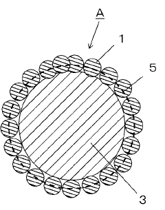
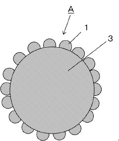
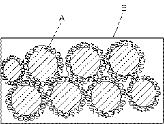
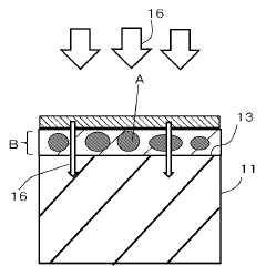
Quantum dot integrated body and quantum dot layer, and solar cell using the same
PatentInactiveJP2014168052A
Innovation
- A quantum dot assembly is formed by adhering quantum dots with a particle size of 10 nm or less to a support with a larger particle size and bandgap, allowing for even arrangement and integration on a curved surface, enhancing electron confinement and absorption efficiency.
Quantum dots absorbing and emitting multiple photons and preparing method of the same
PatentInactiveKR1020230062983A
Innovation
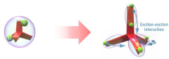
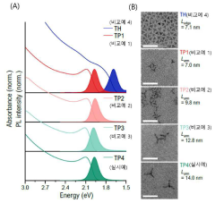
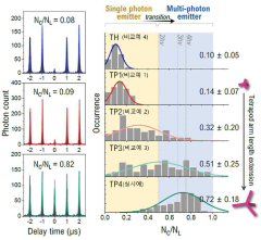
- Development of tetrapod-shaped quantum dots with multiple arms, each capable of absorbing and emitting multiple photons, and a method for synthesizing these quantum dots through controlled precursor reactions and post-processing.
Fabrication Techniques for Quantum Dot Systems
The fabrication of quantum dot systems for topological photonic integration represents a critical technological challenge that requires precision engineering at the nanoscale. Current fabrication techniques can be broadly categorized into top-down and bottom-up approaches, each with distinct advantages for specific applications in topological photonics.
Molecular Beam Epitaxy (MBE) remains the gold standard for high-quality quantum dot fabrication, offering atomic-level precision and exceptional purity. This technique enables the growth of self-assembled quantum dots with well-controlled size distributions and spatial arrangements, critical for maintaining coherent quantum states in topological photonic circuits. Recent advancements in MBE have achieved dot densities exceeding 10^11 cm^-2 with size variations below 5%.
Chemical Vapor Deposition (CVD) techniques provide a more cost-effective alternative, though with some compromise in precision. Modified CVD processes incorporating strain-engineered substrates have demonstrated promising results for creating ordered quantum dot arrays suitable for topological edge state applications. The scalability of CVD makes it particularly attractive for industrial implementation.
Lithographic patterning combined with etching processes offers another approach for quantum dot fabrication. Electron-beam lithography can achieve feature sizes below 10 nm, enabling precise positioning of quantum dots within photonic crystal structures. This deterministic placement is essential for creating topologically protected light pathways with minimal scattering losses.
Colloidal synthesis methods have emerged as versatile techniques for producing solution-processable quantum dots with tunable optical properties. These chemically synthesized nanocrystals can be integrated into polymer matrices or deposited as thin films, offering new possibilities for flexible topological photonic devices. Recent developments in ligand engineering have significantly improved the quantum efficiency and stability of colloidal quantum dots.
Integration challenges remain significant, particularly regarding the precise alignment of quantum dots with photonic crystal structures to maintain topological protection. Advanced pick-and-place techniques using atomic force microscopy tips have demonstrated promising results for deterministic integration but face throughput limitations for large-scale production.
The development of hybrid fabrication approaches combining multiple techniques shows particular promise. For example, template-assisted self-assembly methods leverage the precision of lithography with the scalability of bottom-up growth, potentially offering the best compromise for practical applications in topological photonic integration.
Quantum Security Applications & Standards
The integration of quantum dot systems with topological photonics has significant implications for quantum security applications and standards. Current quantum security protocols predominantly rely on quantum key distribution (QKD) methods, which can be substantially enhanced through topological protection mechanisms offered by quantum dot-based photonic systems. These systems provide inherent resistance against decoherence and backscattering, critical vulnerabilities in conventional quantum communication channels.
Industry standards for quantum security are rapidly evolving, with organizations such as NIST, ETSI, and ISO developing frameworks that increasingly recognize the importance of topologically protected quantum states. The unique band structure and edge states in topological photonic systems enable robust quantum bit transmission with significantly reduced error rates compared to traditional photonic implementations, potentially meeting the stringent requirements of emerging quantum security standards.
Quantum dot systems in topological photonic platforms offer promising applications in quantum random number generation (QRNG), a fundamental component of cryptographic systems. The quantum emission properties of these dots, when coupled with topological waveguides, produce truly random numbers that are verifiably unpredictable and resistant to side-channel attacks, addressing key concerns in current security certification processes.
Authentication protocols leveraging quantum signatures can be implemented more reliably using topological photonic circuits with embedded quantum dots. These systems enable the creation of unforgeable quantum tokens based on the impossibility of perfectly cloning unknown quantum states, while the topological protection ensures the integrity of the quantum information during processing and transmission.
Post-quantum cryptography standards are increasingly considering hardware implementations that can resist both classical and quantum attacks. Topological photonic quantum dot systems represent a promising hardware platform for implementing these advanced cryptographic primitives, offering inherent protection against certain classes of side-channel attacks due to their robust transport properties.
The standardization landscape for quantum security technologies is becoming more receptive to topological approaches, with recent technical committees specifically addressing the integration of topological protection in quantum communication protocols. This trend suggests that quantum dot systems in topological photonic platforms may soon become a recognized standard component in quantum-secure networks, particularly for critical infrastructure applications requiring maximum security assurance.
Unlock deeper insights with PatSnap Eureka Quick Research — get a full tech report to explore trends and direct your research. Try now!
Generate Your Research Report Instantly with AI Agent
Supercharge your innovation with PatSnap Eureka AI Agent Platform!