

Establish Atomic Force Microscopy For Nano-manufacturing Environments
SEP 19, 202510 MIN READ
Generate Your Research Report Instantly with AI Agent
Patsnap Eureka helps you evaluate technical feasibility & market potential.
AFM Technology Background and Objectives
Atomic Force Microscopy (AFM) emerged in the mid-1980s as a revolutionary imaging technique capable of visualizing surfaces at the nanoscale. Developed by Gerd Binnig, Calvin Quate, and Christoph Gerber in 1986, AFM evolved from Scanning Tunneling Microscopy (STM) to overcome limitations in material conductivity requirements. Unlike electron microscopy techniques, AFM offers the unique advantage of three-dimensional surface profiling with extraordinary resolution without requiring vacuum conditions or sample conductivity.
The evolution of AFM technology has been marked by significant advancements in probe design, feedback systems, and operational modes. From its initial contact mode operation, AFM has expanded to include tapping mode, non-contact mode, and various specialized techniques that enable not only topographical imaging but also measurement of mechanical, electrical, magnetic, and chemical properties at the nanoscale.
Recent technological developments have focused on increasing scanning speeds, improving resolution, and enhancing automation capabilities. High-speed AFM now allows for real-time observation of dynamic processes at the molecular level, while multifrequency techniques have expanded the range of simultaneously measurable properties. These advancements have gradually transformed AFM from a purely scientific instrument to a potential manufacturing tool.
The integration of AFM into nano-manufacturing environments represents the next frontier in precision manufacturing. As industries push toward smaller device dimensions and more precise fabrication requirements, traditional quality control and process monitoring techniques become inadequate. AFM offers the potential to bridge this gap by providing in-line, non-destructive metrology with nanometer-scale resolution.
The primary objective of establishing AFM for nano-manufacturing environments is to develop robust, high-throughput systems capable of operating reliably in industrial settings. This includes creating AFM platforms with significantly faster scanning capabilities, automated operation, and integration with existing manufacturing workflows. Such systems must maintain nanometer-scale precision while handling larger sample sizes and operating under less controlled conditions than laboratory environments.
Additional technical goals include developing specialized probes for manufacturing applications, implementing advanced data processing algorithms for real-time analysis, and creating standardized protocols for measurement and calibration. The ultimate aim is to transform AFM from a specialized laboratory instrument into an essential component of advanced manufacturing processes, enabling quality control, process monitoring, and defect analysis at unprecedented resolution levels.
The successful integration of AFM into nano-manufacturing will support critical advances in semiconductor fabrication, nanomedicine production, advanced materials development, and other emerging high-precision industries where nanoscale features directly impact product performance and reliability.
Nano-manufacturing Market Demand Analysis
The global nano-manufacturing market is experiencing unprecedented growth, driven by increasing demand for miniaturized components across multiple industries. Current market valuations place the nano-manufacturing sector at approximately $25 billion, with projections indicating a compound annual growth rate of 14.3% through 2028. This robust growth trajectory underscores the critical importance of advanced metrology tools like Atomic Force Microscopy (AFM) in supporting quality control and process optimization.
The semiconductor industry represents the largest market segment for nano-manufacturing applications, accounting for nearly 40% of the total market share. As chip manufacturers continue to push the boundaries of Moore's Law with sub-5nm process nodes, the need for precise measurement and characterization tools has become paramount. Industry leaders report that even nanometer-scale variations can significantly impact device performance, creating strong demand for in-line AFM solutions capable of providing real-time feedback during fabrication processes.
Medical and pharmaceutical sectors have emerged as rapidly growing markets for nano-manufacturing technologies, particularly in drug delivery systems and medical implants. The precision offered by AFM in characterizing surface properties directly correlates with biocompatibility and drug release profiles. Market research indicates that pharmaceutical companies are increasing R&D investments in nano-formulations by 18% annually, creating substantial opportunities for AFM integration in production environments.
Consumer electronics manufacturers are increasingly incorporating nano-structured materials to enhance product performance and differentiation. The miniaturization trend in wearable technology and IoT devices has created demand for manufacturing processes capable of consistent sub-micron feature production. Industry surveys reveal that 73% of electronics manufacturers consider advanced metrology tools essential for maintaining competitive advantage in next-generation product development.
Energy sector applications, particularly in battery technology and photovoltaics, represent another significant market driver. The performance of these technologies is heavily dependent on nano-scale structures and interfaces that directly impact efficiency and longevity. Market analysis shows that manufacturers are willing to invest substantially in quality control systems that can reduce defect rates and improve consistency in nano-structured energy materials.
Regional market analysis indicates that Asia-Pacific currently dominates the nano-manufacturing landscape with 45% market share, followed by North America (28%) and Europe (22%). However, the fastest growth is occurring in emerging economies where governments are strategically investing in advanced manufacturing capabilities to move up the value chain in global production networks.
Customer requirements across these diverse markets consistently emphasize the need for AFM systems that can operate in production environments rather than laboratory settings. Key demands include higher throughput, automated operation, integration with existing manufacturing execution systems, and robust performance in non-ideal environmental conditions.
Current AFM Implementation Challenges
Despite significant advancements in Atomic Force Microscopy (AFM) technology, its integration into nano-manufacturing environments faces substantial challenges. The transition from laboratory research settings to industrial production environments introduces complexities that current AFM implementations struggle to address effectively.
The foremost challenge is throughput limitation. Conventional AFM systems operate at scanning speeds that are incompatible with industrial production rates. While laboratory applications can tolerate scan times of several minutes per sample area, manufacturing environments require inspection rates orders of magnitude faster to maintain economically viable production throughput. This fundamental mismatch creates a significant barrier to AFM adoption in manufacturing settings.
Environmental stability presents another critical challenge. Manufacturing facilities typically experience vibrations, acoustic noise, temperature fluctuations, and electromagnetic interference at levels significantly higher than controlled laboratory environments. These disturbances directly impact the nanometer-scale precision of AFM measurements, resulting in degraded image quality and unreliable data acquisition. Current vibration isolation systems for AFM are often bulky, expensive, and insufficient for harsh manufacturing conditions.
Automation and integration capabilities of existing AFM systems remain inadequate for manufacturing workflows. Most commercial AFM platforms require significant operator expertise and manual intervention for sample loading, tip replacement, calibration, and measurement parameter optimization. This high dependency on skilled operators contradicts the automation requirements of modern manufacturing lines, where minimal human intervention is essential for consistent operation.
Reliability and maintenance considerations further complicate industrial AFM implementation. The delicate nature of AFM probes results in frequent tip wear and contamination in production environments, necessitating regular replacement. Current systems lack robust self-diagnostic capabilities and predictive maintenance features that would enable integration into manufacturing execution systems and quality control protocols.
Data processing and interpretation represent additional hurdles. The massive data volumes generated by AFM in a production setting require real-time processing capabilities that exceed what current systems offer. Manufacturing applications demand immediate go/no-go decisions based on measurement results, whereas traditional AFM data analysis often involves time-consuming post-processing and expert interpretation.
Cost considerations remain prohibitive for widespread adoption. The high capital expenditure for AFM instrumentation, combined with significant operational costs related to maintenance, consumables, and specialized operator training, creates unfavorable economics for many potential manufacturing applications. This cost structure limits AFM implementation primarily to high-value products where the enhanced measurement capabilities can justify the investment.
Current AFM Integration Solutions
01 AFM instrumentation and hardware improvements
Various innovations in atomic force microscopy hardware components have been developed to enhance performance and capabilities. These include specialized cantilevers, probe tips, scanning mechanisms, and detection systems that improve resolution, stability, and measurement accuracy. Hardware improvements enable more precise topographical imaging and force measurements at the nanoscale level.- AFM instrumentation and hardware improvements: Advancements in atomic force microscopy hardware components including specialized cantilevers, probes, and detection systems that enhance measurement precision and capabilities. These improvements focus on optimizing the physical components of AFM systems to achieve better resolution, stability, and functionality across various applications.
- AFM measurement techniques and methodologies: Various measurement approaches and methodologies used in atomic force microscopy to characterize different sample properties. These techniques include specialized scanning modes, force measurement protocols, and data acquisition methods that enable researchers to extract specific information about surface topography, mechanical properties, and other physical characteristics.
- Sample preparation and handling for AFM: Methods and systems for preparing, mounting, and manipulating samples for atomic force microscopy analysis. These innovations address challenges in sample positioning, environmental control, and preservation of sample integrity during measurement, which are critical for obtaining accurate and reproducible AFM results.
- AFM data processing and analysis: Software solutions and algorithms for processing, analyzing, and interpreting atomic force microscopy data. These innovations focus on transforming raw AFM measurements into meaningful information through image processing, statistical analysis, and specialized computational methods that enhance data visualization and extraction of quantitative parameters.
- AFM applications in material and biological sciences: Specialized applications of atomic force microscopy in characterizing materials and biological samples. These innovations demonstrate how AFM can be adapted to study specific properties such as surface roughness, mechanical strength, molecular interactions, and cellular structures across various scientific disciplines including nanotechnology, materials science, and life sciences.
02 AFM operational modes and measurement techniques
Different operational modes and measurement techniques have been developed for atomic force microscopy to analyze various sample properties. These include contact mode, tapping mode, non-contact mode, and specialized techniques for measuring electrical, magnetic, mechanical, and chemical properties of surfaces. These methods allow researchers to obtain comprehensive information about sample characteristics at the nanoscale.Expand Specific Solutions03 Sample preparation and handling for AFM
Innovations in sample preparation and handling techniques for atomic force microscopy enable more accurate and reliable measurements. These include methods for immobilizing samples, environmental control systems, liquid cell designs, and approaches for analyzing biological specimens. Proper sample preparation is crucial for obtaining high-quality AFM data and preventing artifacts.Expand Specific Solutions04 AFM data processing and analysis algorithms
Advanced data processing and analysis algorithms have been developed to extract meaningful information from atomic force microscopy measurements. These include noise reduction techniques, image enhancement methods, automated feature recognition, and quantitative analysis tools. Sophisticated software solutions help researchers interpret complex AFM data and derive valuable insights about surface properties.Expand Specific Solutions05 Combined AFM systems with other analytical techniques
Integration of atomic force microscopy with complementary analytical techniques creates powerful hybrid systems for comprehensive sample characterization. These combinations include AFM with optical microscopy, Raman spectroscopy, infrared spectroscopy, and scanning electron microscopy. Such integrated approaches provide correlative information about sample morphology, composition, and properties at multiple length scales.Expand Specific Solutions
Key Industry Players in Nano-manufacturing AFM
Atomic Force Microscopy (AFM) for nano-manufacturing is in a growth phase, with the market expanding as industries recognize its potential for precise surface characterization and manipulation at nanoscale. The global market is projected to reach significant value due to increasing applications in semiconductor, materials science, and biomedical sectors. Technologically, the field shows varying maturity levels across players. Leading research institutions (Tsinghua University, California Institute of Technology) and established manufacturers (Bruker Nano, FEI Co.) demonstrate advanced capabilities, while newer entrants are developing specialized applications. Companies like Seagate Technology and Industrial Technology Research Institute are leveraging AFM for industrial applications, bridging the gap between academic research and commercial implementation. The ecosystem includes both specialized instrument manufacturers and research organizations working on novel methodologies for integrating AFM into production environments.
Bruker Nano, Inc.
Technical Solution: Bruker Nano has developed advanced AFM systems specifically optimized for nano-manufacturing environments, featuring their proprietary PeakForce Tapping technology that enables high-resolution imaging while protecting both tip and sample. Their FastScan systems incorporate real-time drift compensation and automated probe exchange mechanisms to maintain continuous operation in production settings. Bruker's industrial AFM platforms integrate with automated sample handling systems and feature closed-loop positioning with nanometer precision for reliable large-area measurements. Their systems employ machine learning algorithms for defect classification and incorporate environmental control chambers to maintain stable temperature, humidity, and vibration isolation critical for nano-manufacturing processes. Bruker's AFM solutions also feature specialized probes with extended lifetimes designed specifically for industrial inspection applications.
Strengths: Industry-leading resolution capabilities with proprietary PeakForce technology; robust integration with factory automation systems; comprehensive software suite for industrial quality control. Weaknesses: Higher initial investment costs compared to academic-focused systems; requires specialized training for operators; system complexity can increase maintenance requirements.
Industrial Technology Research Institute
Technical Solution: The Industrial Technology Research Institute (ITRI) has developed AFM systems specifically designed for semiconductor manufacturing environments, featuring contamination-resistant components and cleanroom-compatible designs. Their AFM platforms incorporate automated wafer handling capabilities that integrate directly with semiconductor production lines, enabling in-line inspection without manual intervention. ITRI's systems employ specialized algorithms for critical dimension measurements at sub-10nm resolution, essential for advanced semiconductor node manufacturing. They have pioneered high-speed scanning techniques that reduce inspection time while maintaining measurement accuracy, addressing a key challenge in production environments. ITRI's AFM technology includes specialized probes with extended lifetimes designed for silicon wafer inspection and features automated tip conditioning routines that maintain consistent measurement quality throughout extended production runs.
Strengths: Deep integration with semiconductor manufacturing workflows; specialized for cleanroom environments; optimized for high-throughput wafer inspection. Weaknesses: Narrowly focused on semiconductor applications; less adaptable to other nano-manufacturing contexts; requires specialized knowledge of semiconductor processes.
Critical AFM Sensing Technologies
Atomic Force Microscopy System and Method for Nanoscale Measurement
PatentActiveUS20120030846A1
Innovation
- An AFM system with a cantilever and electromagnetic coil that generates a time-varying magnetic field within the sample, allowing for imaging of various properties without bias voltage and using softer cantilevers for higher sensitivity, including electrical, dielectric, and magnetic properties, with a non-magnetic or magnetic tip.
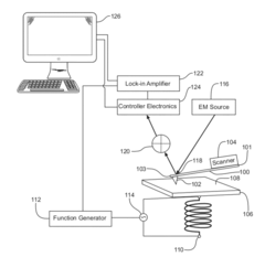
Atomic force microscopes and methods of measuring specimens using the same
PatentInactiveUS20110203020A1
Innovation
- The integration of both short-stroke and long-stroke scanners within an atomic force microscope, utilizing a piezoelectric tube scanner for short-stroke scanning and a flexure scanner for long-stroke scanning, along with a coarse approach system, allows for precise measurement of three-dimensional shapes by enabling simultaneous movement and control of the cantilever's displacement and vibration, using a combination of piezoelectric motors and optical systems for accurate positioning and imaging.


Cleanroom Compatibility Requirements
Integrating Atomic Force Microscopy (AFM) into nano-manufacturing environments necessitates strict adherence to cleanroom compatibility requirements. These requirements are paramount to ensure the integrity of both the AFM measurements and the cleanroom environment itself. Standard cleanroom classifications for nano-manufacturing typically range from ISO Class 5 (Class 100) to ISO Class 3 (Class 1), with AFM systems needing to comply with these stringent particulate control standards.
Material selection for AFM components must prioritize low-outgassing materials to prevent contamination. Stainless steel, certain ceramics, and specialized polymers like PEEK or PTFE are preferred over conventional plastics that may release volatile organic compounds (VOCs). All lubricants used in AFM systems must be vacuum-compatible and have minimal vapor pressure to prevent molecular contamination of sensitive surfaces.
Electrostatic discharge (ESD) protection represents another critical requirement, as nano-scale devices are particularly vulnerable to damage from static electricity. AFM systems must incorporate proper grounding schemes and utilize ESD-safe materials throughout their construction. Additionally, vibration isolation systems must be cleanroom-compatible while maintaining their effectiveness at dampening environmental vibrations that would otherwise compromise measurement accuracy.
Thermal management solutions must avoid forced-air cooling systems that could disturb airflow patterns within the cleanroom. Alternative cooling methods such as liquid cooling or heat pipe technologies offer viable solutions that maintain the laminar flow integrity essential to cleanroom operations. The AFM system's footprint must also be optimized to minimize disruption to cleanroom airflow patterns.
Maintenance protocols require special consideration, with accessible components designed for cleaning with cleanroom-approved solvents. Service access points should be designed to minimize particle generation during routine maintenance procedures. Furthermore, all cables and connectors must utilize cleanroom-compatible materials with minimal particulate generation during connection and disconnection cycles.
Integration with existing cleanroom monitoring systems is essential for real-time verification of environmental conditions during AFM operation. This includes temperature, humidity, and particulate monitoring interfaces. Finally, the AFM system should be designed with modular components that can be separately cleaned and sterilized before introduction into the cleanroom environment, with clear protocols for transferring samples and tools between different cleanroom zones without compromising cleanliness standards.
Throughput Optimization Strategies
Throughput optimization in Atomic Force Microscopy (AFM) for nano-manufacturing environments represents a critical challenge for industrial implementation. Traditional AFM techniques, while offering exceptional resolution, suffer from inherently slow scanning speeds that limit their viability in production settings. Current industrial AFM systems typically achieve scan rates of 1-2 Hz for standard images, resulting in throughput limitations that make comprehensive surface inspection economically unfeasible for many manufacturing applications.
Several promising strategies have emerged to address this throughput bottleneck. High-speed AFM (HS-AFM) technologies have demonstrated scan rates exceeding 100 Hz through the implementation of miniaturized cantilevers with higher resonance frequencies and optimized feedback control algorithms. These systems reduce the mechanical response time and enable faster data acquisition without sacrificing measurement quality.
Parallel probe arrays represent another significant advancement, with systems incorporating multiple cantilevers operating simultaneously to multiply throughput proportionally. Recent developments have demonstrated arrays containing up to 128 independently controlled probes, effectively increasing scanning capacity by two orders of magnitude compared to single-probe systems.
Adaptive scanning methodologies offer complementary benefits by intelligently allocating measurement resources. These approaches utilize real-time data analysis to identify regions of interest requiring high-resolution imaging while rapidly scanning less critical areas at lower resolution. Implementation of machine learning algorithms further enhances this capability by predicting surface features based on partial scan data, reducing the total scan time required for comprehensive characterization.
Hardware optimizations focusing on piezoelectric actuator response times and mechanical stability have yielded substantial improvements. Advanced control systems employing model predictive control and active vibration compensation enable faster stage movements while maintaining positioning accuracy. These developments have reduced settling times by up to 70% in laboratory demonstrations.
Integration of AFM with complementary high-throughput screening techniques presents a hybrid approach worth consideration. By combining AFM with optical or spectroscopic methods for initial rapid screening, manufacturers can strategically deploy high-resolution AFM measurements only where necessary, maximizing information yield while minimizing total inspection time.
The economic implications of these throughput enhancements are substantial. Analysis indicates that achieving scan rates of 20-50 Hz with multi-probe systems could reduce per-unit inspection costs by 85-90%, potentially transforming AFM from a specialized analytical tool to a viable in-line quality control method for nano-manufacturing processes.
Unlock deeper insights with Patsnap Eureka Quick Research — get a full tech report to explore trends and direct your research. Try now!
Generate Your Research Report Instantly with AI Agent
Supercharge your innovation with Patsnap Eureka AI Agent Platform!