

Improve Atomic Force Microscopy System Efficiency — Guide
SEP 19, 20259 MIN READ
Generate Your Research Report Instantly with AI Agent
PatSnap Eureka helps you evaluate technical feasibility & market potential.
AFM Technology Evolution and Objectives
Atomic Force Microscopy (AFM) has evolved significantly since its invention in 1986 by Gerd Binnig, Calvin Quate, and Christoph Gerber. This revolutionary scanning probe microscopy technique has transformed our ability to visualize and manipulate matter at the nanoscale. The technology's evolution has been marked by continuous improvements in resolution, speed, and functionality, enabling researchers to explore surfaces with unprecedented precision.
The initial AFM systems operated primarily in contact mode, where the probe maintained constant contact with the sample surface. This approach, while groundbreaking, presented limitations in terms of sample damage and imaging artifacts. The 1990s witnessed the development of dynamic modes, including tapping mode and non-contact AFM, which significantly reduced sample damage and expanded the range of materials that could be effectively imaged.
A pivotal advancement came with the introduction of high-speed AFM in the early 2000s, which dramatically reduced image acquisition times from minutes to seconds or even milliseconds. This breakthrough enabled the observation of dynamic biological processes in real-time, opening new frontiers in life sciences research. Concurrently, multifrequency and multimodal AFM techniques emerged, allowing simultaneous measurement of multiple sample properties.
The integration of AFM with complementary techniques has been another significant trend. Combinations with optical microscopy, Raman spectroscopy, and infrared spectroscopy have created powerful hybrid systems capable of correlative imaging across multiple length scales and providing chemical specificity alongside topographical information.
Recent years have seen remarkable progress in automation and user-friendly interfaces, making AFM more accessible to non-specialists. Machine learning algorithms have been increasingly incorporated for image processing, feature recognition, and adaptive scanning strategies, enhancing both efficiency and data quality.
The primary objectives for improving AFM system efficiency encompass several dimensions. First, increasing scanning speed without compromising resolution remains a central goal, particularly for studying dynamic processes and high-throughput applications. Second, enhancing probe longevity and reliability is crucial for consistent performance and reduced operational costs. Third, developing more sophisticated feedback mechanisms and control algorithms aims to optimize image acquisition parameters in real-time.
Additionally, improving data processing workflows through automated analysis pipelines seeks to accelerate the extraction of meaningful information from raw AFM data. Finally, integrating AFM systems with complementary characterization techniques continues to be pursued to provide more comprehensive sample analysis within a single experimental setup.
Market Demand Analysis for High-Efficiency AFM Systems
The global market for Atomic Force Microscopy (AFM) systems has been experiencing steady growth, driven primarily by increasing demand in semiconductor manufacturing, materials science research, and life sciences applications. Current market assessments value the AFM market at approximately 500 million USD with projections indicating growth to reach 700 million USD by 2027, representing a compound annual growth rate of around 6.5%.
The demand for high-efficiency AFM systems stems from several key market factors. Research institutions and industrial R&D departments are facing increasing pressure to accelerate their research cycles while maintaining or improving precision. This has created a significant market pull for AFM systems that can deliver faster scanning rates without compromising resolution or accuracy.
In the semiconductor industry, which represents nearly 30% of the AFM market, the continuous miniaturization of components has intensified the need for more efficient metrology tools. As chip manufacturers transition to sub-5nm processes, quality control procedures require more measurements per wafer, making scan speed and throughput critical factors in AFM system selection.
The life sciences sector has emerged as the fastest-growing application area for AFM technology, with estimated growth rates exceeding 8% annually. This growth is fueled by increasing applications in pharmaceutical research, particularly in protein characterization and drug delivery studies. Researchers in this field require systems that can rapidly analyze multiple samples under various environmental conditions while maintaining nanometer-scale resolution.
Materials science applications continue to represent a substantial market segment, with particular emphasis on advanced materials development for energy storage, catalysis, and quantum computing. These applications demand AFM systems capable of efficiently characterizing surface properties across diverse sample types and environmental conditions.
Geographically, North America and Europe currently account for approximately 60% of the global AFM market, though Asia-Pacific regions, particularly China, Japan, and South Korea, are showing the highest growth rates. This regional expansion is driven by increasing investment in semiconductor manufacturing and academic research facilities.
Customer feedback indicates five primary market demands for improved AFM efficiency: faster scan rates without resolution compromise, simplified user interfaces reducing operator expertise requirements, automated calibration and measurement protocols, improved data processing capabilities, and better integration with complementary analytical techniques. Market surveys suggest that systems addressing these needs could command premium pricing of 15-20% above standard systems.
The competitive landscape shows increasing customer preference for integrated solutions that combine high-efficiency AFM capabilities with complementary characterization techniques, suggesting strong market potential for systems that can seamlessly integrate with spectroscopic or electrical measurement capabilities.
Current AFM Technical Limitations and Challenges
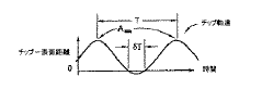
Despite significant advancements in Atomic Force Microscopy (AFM) technology over the past decades, several technical limitations continue to constrain system efficiency and broader application. The most prominent challenge remains scanning speed, with conventional AFM systems typically requiring minutes to hours to generate high-resolution images. This time-consuming process limits throughput in both research and industrial applications, particularly when analyzing dynamic processes or surveying large sample areas.
Resolution limitations present another significant hurdle, especially when attempting to achieve atomic-level imaging while maintaining reasonable scan rates. Current systems face an inherent trade-off between imaging speed and resolution quality, with faster scans often resulting in degraded image quality and increased noise levels. This compromise becomes particularly problematic when investigating nanoscale phenomena that require both high spatial resolution and temporal precision.
Probe wear and sample damage constitute persistent challenges in AFM operation. The mechanical interaction between the probe tip and sample surface inevitably leads to tip degradation over time, altering measurement accuracy and necessitating frequent probe replacement. Additionally, for delicate biological samples or sensitive materials, even minimal contact forces can induce structural alterations, potentially compromising research validity.
Environmental sensitivity further complicates AFM operation, with factors such as temperature fluctuations, acoustic vibrations, and electromagnetic interference significantly affecting measurement stability. Most high-resolution AFM systems require specialized isolation platforms and controlled environments, limiting their deployment in diverse research settings and increasing operational complexity.
Data processing and interpretation remain technically demanding aspects of AFM technology. The vast datasets generated during scanning require sophisticated algorithms for noise reduction, artifact removal, and feature extraction. Current software solutions often lack automation capabilities for routine analysis tasks, requiring significant user expertise and manual intervention.
Calibration and standardization issues persist across different AFM systems and measurement protocols. The lack of universally accepted calibration standards makes cross-comparison between measurements taken on different instruments challenging, hampering collaborative research efforts and technology transfer between institutions.
Integration challenges with complementary analytical techniques represent another limitation. While multimodal approaches combining AFM with optical, spectroscopic, or electrochemical methods offer tremendous potential, technical hurdles in synchronization, data correlation, and compatible sample preparation continue to restrict widespread implementation of these hybrid systems.
Current Approaches to AFM Efficiency Enhancement
01 Advanced scanning techniques for improved efficiency
Various scanning techniques have been developed to enhance the efficiency of atomic force microscopy systems. These include optimized scanning patterns, high-speed scanning methods, and adaptive scanning algorithms that reduce measurement time while maintaining image quality. These techniques allow for faster data acquisition and processing, resulting in more efficient AFM operations and higher throughput for sample analysis.- Improved scanning mechanisms for AFM efficiency: Advanced scanning mechanisms can significantly enhance the efficiency of atomic force microscopy systems. These innovations include optimized probe movement systems, high-speed scanning capabilities, and improved feedback control mechanisms that allow for faster and more precise measurements. These advancements reduce scanning time while maintaining or improving measurement accuracy, enabling more efficient data collection and analysis in AFM applications.
- Enhanced probe design and control systems: Specialized probe designs and control systems can improve the efficiency of atomic force microscopy operations. These include innovations in cantilever design, tip geometry optimization, and advanced probe positioning systems. Improved probe control algorithms allow for more precise movement and faster response times, reducing measurement artifacts and increasing throughput. These enhancements enable more efficient surface characterization and imaging across various sample types.
- Data processing and analysis optimization: Advanced data processing techniques significantly improve the efficiency of atomic force microscopy systems. These include real-time data analysis algorithms, automated feature recognition, and improved signal processing methods that enhance image quality while reducing processing time. Computational optimizations allow for faster conversion of raw measurement data into meaningful results, enabling more efficient interpretation of surface characteristics and properties.
- Environmental control and vibration isolation: Environmental control systems and vibration isolation technologies enhance the efficiency of atomic force microscopy by improving measurement stability and reliability. These systems minimize external disturbances that can affect measurement accuracy, reducing the need for repeated scans and error correction. Advanced isolation platforms and temperature-controlled environments enable more consistent and reproducible results, allowing for more efficient operation in various research and industrial settings.
- Hybrid and multimodal AFM techniques: Hybrid and multimodal approaches combine atomic force microscopy with complementary techniques to increase system efficiency. These integrated systems allow for simultaneous measurement of multiple sample properties in a single scan, reducing overall analysis time. Combined measurement modes enable more comprehensive sample characterization without the need for separate instruments or sequential measurements, significantly improving workflow efficiency in materials research and nanoscale analysis.
02 Probe design and optimization for enhanced performance
Innovations in probe design significantly impact AFM system efficiency. Advanced probe materials, geometries, and coatings improve tip-sample interactions, reduce wear, and enhance measurement sensitivity. Optimized cantilever designs with specific spring constants and resonance frequencies allow for more precise force control and faster scanning speeds, ultimately improving the overall efficiency of atomic force microscopy systems.Expand Specific Solutions03 Feedback control systems for real-time adjustments
Sophisticated feedback control systems enable real-time adjustments during AFM operation, significantly improving efficiency. These systems continuously monitor and adjust parameters such as tip-sample distance, scanning speed, and applied force to maintain optimal imaging conditions. Advanced algorithms for PID control and adaptive feedback mechanisms reduce artifacts, minimize sample damage, and allow for faster scanning without compromising data quality.Expand Specific Solutions04 Integration of multiple measurement modes
Modern AFM systems integrate multiple measurement modes into a single platform, enhancing operational efficiency. These multimodal systems can seamlessly switch between imaging modes (contact, tapping, non-contact) and simultaneously collect various data types (topography, mechanical properties, electrical characteristics). This integration eliminates the need for multiple separate measurements, reduces sample handling, and provides comprehensive sample characterization in a single experiment.Expand Specific Solutions05 Automated calibration and data processing
Automation of calibration procedures and data processing significantly improves AFM system efficiency. Automated tip calibration, scanner calibration, and drift correction reduce operator intervention and ensure consistent measurement quality. Advanced software algorithms for real-time data processing, feature recognition, and artifact removal streamline the workflow from raw data to meaningful results, enabling higher throughput and more efficient use of instrument time.Expand Specific Solutions
Leading AFM Manufacturers and Research Institutions
The Atomic Force Microscopy (AFM) market is currently in a mature growth phase with increasing demand for higher efficiency systems. The global AFM market is estimated at approximately $500 million, with projected growth driven by semiconductor, materials science, and life sciences applications. Leading commercial players include Bruker Nano, Oxford Instruments Asylum Research, and Hitachi High-Tech Science, who have established strong market positions through advanced hardware solutions. Emerging competitors like Nearfield Instruments and Infinitesima are disrupting the market with innovative high-throughput technologies. Academic and research institutions (CNRS, University of Bristol, Cornell) continue to advance fundamental AFM technologies, while industrial giants (Applied Materials, Keysight Technologies) integrate AFM capabilities into broader metrology solutions. The technology is evolving toward faster scanning, automated operation, and improved data processing to address increasing industrial demands.
Bruker Nano, Inc.
Technical Solution: Bruker has developed PeakForce Tapping technology for atomic force microscopy that enables simultaneous acquisition of multiple sample properties while protecting both tip and sample from damage. Their FastScan technology combines high-speed scanners with low-noise, high-bandwidth electronics and control algorithms to increase imaging speed by up to 20 times compared to conventional AFM systems[1]. Additionally, Bruker's proprietary DataCube Mode allows for capturing complete force curves at each pixel, enabling post-acquisition analysis and extraction of multiple mechanical properties from a single dataset[2]. Their latest systems incorporate machine learning algorithms for automated parameter optimization and feature recognition, reducing operator dependency and increasing throughput. Bruker has also pioneered the integration of photothermal excitation (PeakForce-SECM) to improve cantilever response and measurement stability in liquid environments[3].
Strengths: Industry-leading scan speeds with FastScan technology; comprehensive mechanical property mapping with minimal sample damage; advanced automation features reducing operator expertise requirements. Weaknesses: Premium pricing structure limiting accessibility for smaller research institutions; proprietary software ecosystems can create workflow integration challenges; high-end systems require specialized training despite automation improvements.
Infinitesima Ltd.
Technical Solution: Infinitesima has revolutionized AFM efficiency with their Rapid Probe Microscopy (RPM) technology, specifically designed for semiconductor metrology applications. Their approach uses a resonating probe that maintains continuous contact with the sample surface while scanning at velocities up to 5mm/s, approximately 100 times faster than conventional AFM systems[1]. The RPM technology incorporates a unique optical interferometric detection system that enables high-speed, non-destructive imaging with sub-nanometer resolution. Infinitesima's systems feature specialized probe designs with wear-resistant tips and optimized spring constants to withstand the demands of high-speed operation while maintaining measurement accuracy. Their latest generation systems incorporate parallel processing hardware architectures and real-time data processing algorithms to handle the massive data throughput generated during rapid scanning operations[2]. The company has also developed specialized software tools for automated defect classification and pattern recognition tailored to semiconductor manufacturing environments.
Strengths: Exceptional scanning speed (up to 100x faster than conventional AFM) making it suitable for in-line semiconductor inspection; non-destructive imaging capability preserving sample integrity; specialized for semiconductor industry integration. Weaknesses: Highly specialized for semiconductor applications with limited versatility for other research domains; requires significant capital investment; technology optimization focuses on topographical measurements rather than comprehensive material property characterization.
Key Patents and Innovations in AFM Scanning Techniques
Scanning probe microscope and method of operating the same
PatentActiveJP2018036272A
Innovation
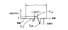
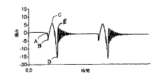
- The implementation of Peak Force Tapping (PFT) Mode, which uses instantaneous interaction force control to minimize parasitic coupling and automate feedback adjustments, allowing for high-resolution imaging with minimal user intervention and reduced tip-sample forces.
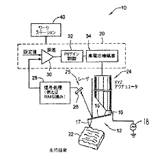
Fast-scanning SPM and method of operating same
PatentActiveEP2183569A2
Innovation
- A fast-scanning SPM system with a high-bandwidth probe and scanner, employing a force control loop with a bandwidth of up to 100 kHz, a stiff and lightweight tip scanner with a high fundamental resonant frequency, and integrated optics for precise feedback control, enabling rapid scanning with minimal noise and damage prevention.
AFM Integration with Complementary Microscopy Methods
The integration of Atomic Force Microscopy (AFM) with complementary microscopy methods represents a significant advancement in microscopy technology, enabling researchers to obtain comprehensive multi-dimensional data from samples. This integration approach combines the nanoscale resolution and force measurement capabilities of AFM with other microscopy techniques such as optical microscopy, electron microscopy, and spectroscopic methods.
Correlative microscopy, which combines AFM with optical microscopy (particularly confocal microscopy), has gained substantial traction in biological research. This integration allows simultaneous visualization of cellular structures and measurement of their mechanical properties. The technical implementation typically involves specialized sample stages that enable precise alignment between the two systems, with software solutions that facilitate data correlation and overlay.
AFM-SEM (Scanning Electron Microscopy) and AFM-TEM (Transmission Electron Microscopy) integrations have revolutionized materials science research by providing complementary information about surface topography, composition, and internal structure. These hybrid systems often require sophisticated vacuum-compatible AFM components and precise sample transfer mechanisms to maintain sample integrity between different imaging environments.
Recent developments in AFM-Raman integration have enabled chemical mapping with nanoscale spatial resolution. The tip-enhanced Raman spectroscopy (TERS) approach uses the AFM tip as a plasmonic antenna to enhance Raman signals from the sample area directly beneath the tip, achieving chemical specificity beyond the diffraction limit of conventional optical techniques.
Integration challenges primarily involve alignment precision, data registration, and environmental control. Manufacturers like Bruker, Oxford Instruments, and JPK Instruments have developed specialized solutions including unified software platforms that streamline workflow between different microscopy techniques and automated calibration procedures to ensure accurate correlation of multi-modal data.
The efficiency gains from these integrated approaches are substantial. Research indicates that correlative microscopy can reduce total analysis time by up to 40% compared to sequential use of individual techniques. More importantly, the complementary data obtained often reveals structure-function relationships that would remain hidden when using single-modality approaches.
Future development trends point toward fully automated multi-modal imaging platforms with artificial intelligence-driven data integration and analysis. These systems will likely incorporate real-time correlation capabilities, allowing researchers to dynamically adjust measurement parameters based on feedback from complementary techniques, further enhancing AFM system efficiency and expanding its application scope.
Nanoscale Metrology Standards and Calibration Protocols
Nanoscale metrology standards and calibration protocols are fundamental to ensuring the accuracy, reliability, and reproducibility of Atomic Force Microscopy (AFM) measurements. These standards provide reference points against which AFM systems can be calibrated, allowing for consistent measurements across different instruments and laboratories.
The development of robust calibration protocols has evolved significantly over the past decade, with international organizations such as NIST (National Institute of Standards and Technology), PTB (Physikalisch-Technische Bundesanstalt), and ISO (International Organization for Standardization) establishing comprehensive guidelines. These protocols typically address three critical dimensions of AFM calibration: lateral (x-y) calibration, vertical (z) calibration, and probe characterization.
Standard reference materials (SRMs) play a crucial role in AFM calibration. Silicon gratings with precisely defined pitch values serve as common lateral calibration standards, while step height standards, often made from silicon or quartz, are used for vertical calibration. Recent advancements have introduced more sophisticated 3D calibration artifacts that allow simultaneous calibration of all three spatial dimensions.
Traceability to SI units remains a cornerstone of nanoscale metrology. Modern calibration protocols emphasize establishing unbroken chains of comparisons to primary standards maintained by national metrology institutes. This traceability ensures that measurements made on AFM systems can be directly compared to those made using other techniques or in different laboratories.
Environmental factors significantly impact AFM measurements at the nanoscale. Temperature fluctuations, humidity changes, and vibrations can introduce substantial measurement errors. Advanced calibration protocols now incorporate environmental monitoring and correction factors to account for these variables, enhancing measurement reliability across different operating conditions.
Tip characterization represents another critical aspect of AFM calibration. Blind tip reconstruction algorithms and tip characterization standards have become increasingly sophisticated, allowing for more accurate compensation of tip-sample convolution effects that can distort AFM images and measurements.
Interlaboratory comparison studies have demonstrated that properly implemented calibration protocols can reduce measurement uncertainty from tens of percent to below 1% for many common AFM measurements. These improvements directly translate to enhanced AFM system efficiency by reducing the need for repeated measurements and providing greater confidence in experimental results.
Unlock deeper insights with PatSnap Eureka Quick Research — get a full tech report to explore trends and direct your research. Try now!
Generate Your Research Report Instantly with AI Agent
Supercharge your innovation with PatSnap Eureka AI Agent Platform!