

How To Adapt Atomic Force Microscopy To New Material Types — Techniques
SEP 19, 20259 MIN READ
Generate Your Research Report Instantly with AI Agent
Patsnap Eureka helps you evaluate technical feasibility & market potential.
AFM Technology Evolution and Objectives
Atomic Force Microscopy (AFM) has evolved significantly since its invention in 1986 by Gerd Binnig, Calvin Quate, and Christoph Gerber. Initially designed to overcome the limitations of Scanning Tunneling Microscopy (STM) for non-conductive samples, AFM has transformed into a versatile tool capable of imaging, measuring, and manipulating matter at the nanoscale. The technology's evolution has been marked by continuous improvements in resolution, speed, and functionality, enabling researchers to explore increasingly complex material systems.
The early generations of AFM were primarily focused on topographical imaging in ambient conditions, with limited capabilities for specialized materials. As research demands grew, AFM technology expanded to accommodate various operational modes, including contact, non-contact, and tapping modes, each offering distinct advantages for different material types. The introduction of liquid-cell AFM in the 1990s represented a significant breakthrough, allowing for the examination of biological samples in their native environments.
Recent technological advancements have led to the development of multimodal AFM systems capable of simultaneously measuring multiple sample properties, such as mechanical, electrical, magnetic, and thermal characteristics. These developments have been crucial for the characterization of novel materials like 2D materials, biomaterials, and complex nanocomposites that exhibit unique surface properties and require specialized measurement approaches.
The primary objective of modern AFM adaptation is to overcome the inherent limitations when examining diverse material types. These challenges include minimizing tip-sample interactions that can damage delicate materials, enhancing measurement accuracy on heterogeneous surfaces, and developing protocols for materials with extreme properties (highly hydrophobic/hydrophilic, electrically charged, or magnetically active surfaces).
Another critical goal is to improve the quantitative reliability of AFM measurements across different material systems. This involves developing robust calibration methods, standardizing measurement protocols, and creating reference materials that can validate results across different instruments and laboratories. The scientific community is actively working toward establishing international standards for AFM measurements to ensure reproducibility and comparability of results.
Looking forward, the field aims to integrate AFM with complementary analytical techniques, creating hybrid systems that can provide comprehensive material characterization at multiple length scales. The convergence of AFM with spectroscopic methods, electron microscopy, and computational modeling represents a promising direction for overcoming current limitations and expanding the application scope of AFM to emerging material classes.
Market Applications for Advanced Material Characterization
The advanced material characterization market is experiencing robust growth, driven by increasing demand across multiple industries for precise analysis of novel materials. The global market for material characterization equipment was valued at approximately $5.7 billion in 2022 and is projected to reach $8.3 billion by 2027, growing at a CAGR of 7.8%. This growth reflects the critical importance of techniques like Atomic Force Microscopy (AFM) in modern materials science and engineering.
Semiconductor and electronics industries represent the largest application segment, accounting for nearly 30% of the market share. As device miniaturization continues and new semiconductor materials emerge, AFM techniques provide crucial nanoscale characterization capabilities for quality control and R&D. The ability to measure surface roughness, defects, and electrical properties at atomic resolution makes AFM indispensable for next-generation semiconductor development.
The pharmaceutical and life sciences sectors have emerged as rapidly growing markets for advanced characterization techniques. AFM applications in drug delivery systems, biomaterials, and cellular studies have expanded significantly, with particular value in analyzing soft, biological materials that traditional microscopy techniques might damage. This sector is expected to grow at over 9% annually through 2027, outpacing the overall market.
Energy materials represent another high-growth application area, particularly for battery technology, photovoltaics, and fuel cells. AFM techniques provide critical insights into surface morphology, mechanical properties, and electrochemical characteristics of these materials. With global renewable energy investments exceeding $500 billion annually, demand for specialized material characterization continues to accelerate in this sector.
Aerospace and automotive industries increasingly rely on advanced characterization for lightweight composites, high-performance alloys, and smart materials. AFM techniques help evaluate surface treatments, coating uniformity, and mechanical properties at micro and nanoscales. The push toward electric vehicles and more fuel-efficient aircraft has intensified the need for sophisticated material analysis.
Academic and research institutions remain significant consumers of advanced characterization technologies, driving fundamental materials science discoveries. Government funding for nanotechnology research, estimated at over $10 billion globally, continues to support instrument acquisition and method development.
Emerging applications in quantum materials, 2D materials, and metamaterials are creating new market opportunities for specialized AFM techniques. These novel material systems require advanced characterization capabilities to understand their unique properties and behavior, stimulating innovation in AFM methodology and instrumentation.
Current AFM Limitations with Novel Materials
Despite significant advancements in Atomic Force Microscopy (AFM) technology, several critical limitations persist when applying these techniques to novel materials. The fundamental challenge lies in the probe-sample interaction mechanisms, which were originally optimized for conventional materials with well-understood mechanical and surface properties. When confronted with emerging materials such as 2D materials, soft biological samples, or complex nanocomposites, traditional AFM methodologies often produce artifacts or fail to capture accurate topographical and mechanical information.
One significant limitation is tip-induced deformation, particularly problematic with ultra-soft materials or those with unique surface chemistries. The standard silicon or silicon nitride tips can exert forces that irreversibly alter the sample's native structure, compromising measurement accuracy. This becomes especially pronounced when examining materials with heterogeneous mechanical properties or those existing at interfaces between different phases.
Resolution boundaries present another challenge, particularly for materials with atomic-scale features of interest. While atomic resolution is achievable under ideal conditions, maintaining this precision across diverse material types remains difficult. Novel materials often exhibit complex surface reconstructions, defect structures, or atomic arrangements that conventional AFM struggles to resolve consistently, especially under ambient or liquid conditions necessary for certain material types.
Environmental sensitivity constitutes a major hurdle for AFM characterization of reactive or environmentally responsive materials. Many novel materials require specific atmospheric conditions, temperature ranges, or chemical environments to maintain their native properties. Standard AFM setups lack the environmental control systems necessary to accommodate these requirements, leading to measurements that may not reflect the material's actual behavior in application environments.
Data interpretation frameworks developed for conventional materials often prove inadequate for novel material systems. The complex force interactions between the probe and unconventional materials create signal patterns that existing models cannot accurately interpret. This leads to systematic errors in property extraction and topographical reconstruction, particularly for materials with anisotropic properties or those exhibiting quantum mechanical effects at the nanoscale.
Feedback loop optimization presents technical difficulties when scanning materials with extreme property gradients or discontinuities. The standard PID control parameters that work well for homogeneous samples often fail to maintain stable imaging conditions across heterogeneous novel materials, resulting in scan instabilities, tip crashes, or loss of contact with the sample surface.
These limitations collectively impede the widespread application of AFM techniques to emerging material classes, creating a technological gap between material innovation and characterization capabilities that must be addressed through adaptive instrumentation and methodology development.
Contemporary AFM Modification Approaches
01 Probe and Tip Modifications for AFM
Various modifications to atomic force microscopy probes and tips enhance measurement capabilities and accuracy. These adaptations include specialized tip geometries, coatings, and functionalization techniques that improve resolution, reduce wear, and enable specific interactions with sample surfaces. Modified probes can be designed for particular applications such as biological samples, nanomechanical measurements, or chemical sensing.- Probe and tip modifications for AFM: Various modifications to atomic force microscopy probes and tips enhance measurement capabilities and accuracy. These adaptations include specialized coatings, functionalized tips, and novel probe designs that improve resolution, sensitivity, and specificity for different sample types. Modified probes can be tailored for specific applications such as biological samples, nanomaterials, or semiconductor surfaces, allowing for more precise measurements of surface properties.
- Environmental and operational adaptations: Adaptations to the operating environment of atomic force microscopes significantly enhance their performance. These include temperature control systems, vibration isolation mechanisms, and atmospheric or liquid medium controls that stabilize measurements. Such environmental adaptations minimize external interference and allow for in-situ measurements under various conditions, including extreme temperatures, vacuum, or liquid environments, expanding the range of samples that can be accurately analyzed.
- Advanced measurement modes and techniques: Novel measurement modes extend the capabilities of atomic force microscopy beyond traditional topographical imaging. These include techniques for measuring electrical, magnetic, mechanical, and chemical properties simultaneously with topography. Adaptations such as force spectroscopy, conductive AFM, magnetic force microscopy, and kelvin probe force microscopy provide multidimensional data about sample characteristics at the nanoscale, enabling more comprehensive material analysis.
- Signal processing and feedback control improvements: Advanced signal processing algorithms and feedback control systems enhance the resolution, speed, and reliability of atomic force microscopy. These adaptations include real-time data filtering, noise reduction techniques, and adaptive feedback mechanisms that optimize the tip-sample interaction. Improved control systems allow for faster scanning rates while maintaining high resolution, and can compensate for instrument drift and other measurement artifacts.
- Integration with complementary techniques: Combining atomic force microscopy with other analytical methods creates powerful hybrid instruments with enhanced capabilities. These integrated systems may incorporate optical microscopy, Raman spectroscopy, infrared spectroscopy, or scanning electron microscopy. Such combinations allow for correlative analysis, providing complementary information about sample properties and enabling more comprehensive characterization of materials at multiple length scales and through different physical phenomena.
02 Environmental and Sample Condition Control Systems
Adaptations that control the environment around the AFM sample improve measurement stability and enable specialized applications. These systems regulate temperature, humidity, atmospheric composition, or introduce liquid environments. Such controls allow for in-situ measurements under varying conditions, making it possible to study dynamic processes, biological samples in near-native states, or materials under specific environmental stresses.Expand Specific Solutions03 Advanced Feedback and Control Mechanisms
Sophisticated feedback and control systems enhance AFM performance by improving stability, speed, and measurement accuracy. These adaptations include high-speed controllers, adaptive feedback algorithms, and noise reduction techniques. Advanced control mechanisms allow for faster scanning, reduced tip-sample forces, and the ability to track rapidly changing surface features, significantly expanding AFM capabilities for dynamic measurements.Expand Specific Solutions04 Multimodal and Hybrid AFM Techniques
Hybrid systems combine AFM with complementary analytical techniques to provide multidimensional characterization of samples. These adaptations integrate optical, spectroscopic, or electrical measurement capabilities with traditional AFM. Such multimodal approaches allow simultaneous acquisition of topographical, mechanical, electrical, thermal, or chemical information, providing comprehensive sample analysis beyond what standard AFM can achieve.Expand Specific Solutions05 High-Speed and Automated AFM Systems
Adaptations focused on increasing scanning speed and automation enhance throughput and reduce operator dependency. These systems incorporate optimized scanners, parallel probes, or automated alignment and calibration procedures. High-speed AFM enables the observation of dynamic processes at nanoscale, while automated systems improve reproducibility and allow for large-area mapping with minimal human intervention.Expand Specific Solutions
Leading Manufacturers and Research Institutions
The Atomic Force Microscopy (AFM) adaptation market is currently in a growth phase, with increasing applications across diverse material types driving innovation. The market is expanding as new materials require specialized AFM techniques, with an estimated global microscopy market exceeding $7 billion. Technologically, the field shows varying maturity levels, with established players like IBM and Applied Materials focusing on industrial applications, while research institutions such as CSIC, University of California, and CNRS lead academic innovation. Emerging players like GLOBALFOUNDRIES and Samsung are integrating AFM into semiconductor manufacturing processes. Collaboration between academic institutions (Beihang University, Wuhan University) and industry leaders is accelerating technique development for novel materials, particularly in nanomaterials and biological samples.
Consejo Superior de Investigaciones Científicas
Technical Solution: CSIC has developed a comprehensive multimodal AFM platform specifically designed for challenging new materials characterization. Their approach integrates traditional AFM with advanced spectroscopic techniques through a novel optical path design that enables simultaneous acquisition of nanomechanical and chemical information[1]. For soft and biological materials, CSIC has pioneered a "minimal force imaging" protocol that dynamically adjusts cantilever parameters based on real-time feedback from the sample, preventing deformation while maintaining resolution[3]. Their system incorporates specialized probes with functionalized tips that can be tailored to specific material interactions, particularly valuable for selective chemical mapping of complex composite materials[5]. CSIC has also developed advanced environmental control chambers allowing precise regulation of temperature, humidity, and gas composition during imaging, enabling in-situ studies of material responses to environmental changes[7]. Additionally, their implementation of high-speed data processing algorithms enables real-time correction of thermal drift and other artifacts, significantly improving measurement accuracy for time-sensitive experiments on reactive or unstable new materials.
Strengths: Exceptional versatility across diverse material types from ultra-soft biological samples to hard inorganic surfaces; superior integration of complementary analytical techniques; advanced environmental control capabilities for realistic testing conditions. Weaknesses: Complex system requiring significant expertise to fully utilize all capabilities; longer setup and calibration times compared to conventional AFM; higher initial investment and maintenance costs due to multimodal integration.
Centre National de la Recherche Scientifique
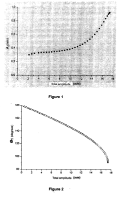
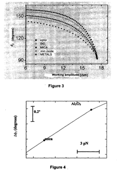
Technical Solution: CNRS has developed advanced multimodal AFM techniques that combine traditional force measurements with simultaneous spectroscopic analysis for new material characterization. Their approach integrates Raman spectroscopy with AFM (Tip-Enhanced Raman Spectroscopy or TERS) to provide chemical composition information alongside topographical data at nanoscale resolution[1]. For soft and biological materials, CNRS has pioneered liquid-phase AFM methods with specialized cantilevers and force modulation techniques that minimize sample damage while maintaining resolution[3]. They've also developed advanced feedback control algorithms that automatically adjust scanning parameters based on real-time material response, particularly useful for heterogeneous samples with varying mechanical properties[5]. Their PeakForce QNM (Quantitative Nanomechanical Mapping) implementation allows simultaneous acquisition of topography and mechanical properties including adhesion, deformation, and elastic modulus across diverse material types.
Strengths: Superior integration of complementary analytical techniques providing multidimensional characterization data; exceptional adaptability to diverse sample environments including liquid, vacuum, and variable temperatures. Weaknesses: Higher technical complexity requiring specialized training; more expensive implementation compared to standard AFM systems; longer acquisition times for multimodal measurements potentially limiting throughput.
Breakthrough AFM Probe Technologies
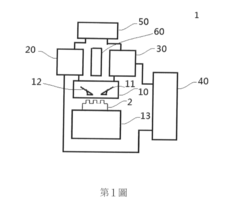
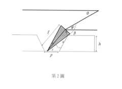
Scanning method for an atomic force microscopy
PatentActiveTW201625955A
Innovation
- An atomic force microscope scanning method using dual probes with adjustable inclination angles to scan a test piece, merging scanning data to enhance accuracy.
Method of using an atomic force microscope and microscope
PatentInactiveEP1912055A1
Innovation
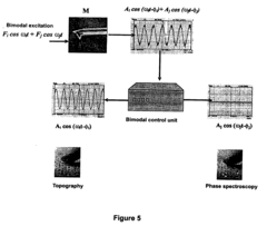
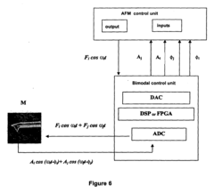
- Simultaneously exciting multiple natural vibration modes of the microlever in an AFM, allowing for separate analysis of amplitude and phase variations to distinguish topographical and compositional information, enhancing sensitivity and accuracy by utilizing higher frequency modes for property measurement.
Nanoscale Measurement Standards and Calibration
Nanoscale measurement standards and calibration represent a critical foundation for the advancement of atomic force microscopy (AFM) techniques across diverse material types. The establishment of reliable measurement standards at the nanoscale has evolved significantly over the past decade, with international metrology organizations developing certified reference materials specifically designed for AFM calibration.
Current nanoscale calibration standards include silicon gratings with precisely defined pitch values, step height standards made from silicon or quartz, and nanoparticle size standards. These standards enable the three-dimensional calibration of AFM instruments, ensuring measurement accuracy across different material interfaces and topographies. The National Institute of Standards and Technology (NIST) and the Physikalisch-Technische Bundesanstalt (PTB) have been instrumental in developing traceable standards that maintain consistency across different laboratory environments.
Calibration methodologies for new material types require consideration of material-specific interactions with the AFM probe. For soft materials like polymers or biological samples, calibration must account for probe-induced deformation, requiring specialized force calibration protocols. Similarly, for highly conductive or magnetic materials, additional calibration steps are necessary to compensate for long-range forces that can influence measurement accuracy.
Recent advances in calibration techniques include the development of in-situ calibration methods that allow for real-time correction of thermal drift and piezoelectric creep effects. These approaches are particularly valuable when working with novel material systems that may exhibit unique thermal or mechanical responses during measurement. Additionally, algorithmic calibration methods have emerged that can compensate for systematic errors through mathematical modeling of the measurement process.
The traceability chain for nanoscale measurements has been strengthened through international comparison studies and round-robin tests. These collaborative efforts have established uncertainty budgets for various AFM measurement modes, providing researchers with quantitative assessments of measurement reliability when adapting techniques to new material types.
Looking forward, the integration of machine learning approaches with calibration protocols shows promise for automating the adaptation of AFM parameters to specific material properties. This could significantly reduce the expertise barrier for applying AFM to novel materials while improving measurement reproducibility. Additionally, the development of multi-parameter reference materials that simultaneously calibrate multiple AFM measurement channels (topography, mechanical, electrical, thermal) represents an important frontier for comprehensive instrument calibration.
Environmental Factors Affecting AFM Performance
Atomic Force Microscopy (AFM) performance is significantly influenced by various environmental factors that must be carefully controlled to ensure accurate measurements, especially when adapting the technique to new material types. Temperature fluctuations represent one of the most critical environmental variables affecting AFM operation. Even minor temperature changes can cause thermal drift in the cantilever and sample, resulting in dimensional instability and image distortion. For high-resolution imaging of novel materials, temperature stability within ±0.1°C is often necessary.
Humidity levels similarly impact AFM measurements by altering the meniscus forces between the tip and sample surface. In high humidity environments, water condensation at the tip-sample interface can create capillary forces that interfere with true topographical measurements. Conversely, extremely low humidity may generate problematic electrostatic charges, particularly when examining insulating materials or polymers with unique surface properties.
Acoustic vibrations and mechanical noise constitute another significant environmental challenge. External vibrations from laboratory equipment, building systems, or human activity can be transmitted to the AFM system, causing resolution degradation. This becomes particularly problematic when examining nanoscale features of novel materials where atomic-level resolution is required. Implementation of vibration isolation systems, including active pneumatic tables or passive dampening platforms, is essential for mitigating these effects.
Air quality and particulate contamination must also be considered when adapting AFM to new material types. Airborne particles can adhere to either the sample surface or the AFM tip, creating imaging artifacts or potentially damaging delicate sample surfaces. For particularly sensitive new materials, operation within cleanroom environments or under controlled atmospheric conditions may be necessary to maintain measurement integrity.
Electromagnetic interference (EMI) represents a less obvious but equally important environmental factor. The sensitive electronic components in modern AFM systems can be affected by electromagnetic fields generated by nearby electronic equipment. When working with materials that have unique electrical or magnetic properties, EMI shielding becomes particularly important to prevent signal distortion and ensure accurate characterization of the material's intrinsic properties.
Atmospheric pressure and composition can also influence AFM performance, particularly for materials with reactive surfaces or those requiring specific atmospheric conditions to maintain their structural integrity. Some advanced AFM systems now incorporate environmental chambers that allow for controlled gas composition, pressure, and even liquid environments to accommodate the specific requirements of novel material types.
Unlock deeper insights with Patsnap Eureka Quick Research — get a full tech report to explore trends and direct your research. Try now!
Generate Your Research Report Instantly with AI Agent
Supercharge your innovation with Patsnap Eureka AI Agent Platform!