

Atomic Force Microscopy Vs Transmission Electron Microscopy: Application
SEP 19, 20259 MIN READ
Generate Your Research Report Instantly with AI Agent
Patsnap Eureka helps you evaluate technical feasibility & market potential.
AFM and TEM Technology Background and Objectives
Atomic Force Microscopy (AFM) and Transmission Electron Microscopy (TEM) represent two cornerstone technologies in the field of nanoscale imaging and characterization. Developed in the 1980s, AFM emerged as a revolutionary scanning probe technique capable of generating three-dimensional surface topography with nanometer resolution. TEM, with earlier origins dating back to the 1930s, has evolved to provide unparalleled internal structural information at atomic scales through electron beam transmission.
The evolution of these technologies has been marked by continuous refinement in resolution capabilities, operational modes, and application versatility. AFM has progressed from basic contact mode operations to advanced multimodal capabilities including force spectroscopy, electrical characterization, and biological imaging in liquid environments. Similarly, TEM has advanced from conventional bright-field imaging to sophisticated techniques such as high-resolution TEM (HRTEM), scanning TEM (STEM), and electron energy loss spectroscopy (EELS).
Current technological trends indicate a convergence of complementary capabilities, with hybrid systems and correlative microscopy approaches gaining prominence. The integration of in-situ environmental controls in both technologies has expanded their application from static structural analysis to dynamic process observation under various conditions, including temperature variations, mechanical stress, and chemical reactions.
The primary objective of modern AFM and TEM development is to overcome their respective limitations while maximizing their inherent strengths. For AFM, this includes enhancing imaging speed, expanding the range of measurable physical properties, and improving resolution in liquid environments for biological applications. For TEM, objectives focus on reducing beam damage to sensitive samples, developing more accessible cryo-TEM capabilities, and advancing in-situ experimental platforms.
Both technologies are increasingly being directed toward solving complex interdisciplinary challenges in materials science, semiconductor technology, biological research, and nanotechnology. The ability to characterize materials at atomic and molecular levels has become essential for innovation in fields ranging from drug delivery systems to quantum computing components.
The technical trajectory suggests future developments will emphasize multimodal data acquisition, automated analysis through artificial intelligence, and enhanced accessibility through more user-friendly interfaces and remote operation capabilities. As nanoscale characterization becomes increasingly critical across scientific and industrial domains, AFM and TEM continue to evolve as complementary rather than competing technologies, each offering unique insights into the nanoscale world.
Market Demand Analysis for Nanoscale Imaging
The nanoscale imaging market has witnessed substantial growth in recent years, driven by increasing demand across multiple sectors including semiconductor manufacturing, materials science, life sciences, and nanotechnology research. The global market for nanoscale imaging technologies was valued at approximately $4.3 billion in 2022 and is projected to reach $6.8 billion by 2027, representing a compound annual growth rate of 9.6%.
Both Atomic Force Microscopy (AFM) and Transmission Electron Microscopy (TEM) serve as cornerstone technologies within this market, albeit addressing different needs and applications. Market research indicates that TEM currently holds a larger market share due to its established presence in research institutions and its ability to provide atomic-level resolution imaging of internal structures. However, AFM is experiencing faster growth rates owing to its versatility, lower operational costs, and expanding applications in biological samples.
The semiconductor industry represents the largest end-user segment for nanoscale imaging, accounting for approximately 35% of the total market. As chip manufacturers continue to pursue smaller node sizes following Moore's Law, the demand for high-precision imaging tools capable of nanometer and sub-nanometer resolution continues to surge. Both AFM and TEM play critical roles in semiconductor failure analysis, process control, and research and development activities.
Life sciences and healthcare applications constitute the fastest-growing segment, with a projected CAGR of 12.3% through 2027. This growth is primarily driven by increasing research in cellular biology, protein structure analysis, and drug development. TEM remains essential for visualizing cellular ultrastructure, while AFM has gained traction for its ability to image biological samples in near-native conditions without extensive sample preparation.
Regional analysis reveals that North America and Asia-Pacific dominate the nanoscale imaging market, collectively accounting for over 70% of global demand. Asia-Pacific, particularly China, South Korea, and Taiwan, is expected to witness the highest growth rate due to expanding semiconductor manufacturing capabilities and increasing research investments.
Customer requirements are evolving toward integrated solutions that combine multiple imaging modalities. There is growing demand for correlative microscopy approaches that leverage the complementary strengths of AFM and TEM. Additionally, automation, improved user interfaces, and advanced data analysis capabilities are becoming increasingly important purchasing factors as organizations seek to improve workflow efficiency and extract more value from imaging data.
The COVID-19 pandemic temporarily disrupted supply chains but simultaneously accelerated demand in certain segments, particularly for virus research and vaccine development applications. This has highlighted the critical importance of advanced imaging technologies in addressing global health challenges and is expected to drive sustained investment in this sector.
Current Status and Technical Challenges
Atomic Force Microscopy (AFM) and Transmission Electron Microscopy (TEM) represent two cornerstone technologies in modern nanoscale imaging and characterization. Currently, both technologies have achieved remarkable advancements but face distinct technical challenges that influence their application domains.
AFM technology has reached a resolution capability of approximately 0.1-1 nm laterally and 0.01 nm vertically under optimal conditions. Recent developments have expanded AFM's functionality beyond topographical imaging to include mechanical, electrical, magnetic, and thermal property measurements through various specialized modes. The global AFM market was valued at approximately $570 million in 2022, with a projected CAGR of 6.8% through 2030, indicating strong commercial adoption across research and industrial sectors.
Despite these advancements, AFM faces several significant technical challenges. Scan speed limitations remain a persistent issue, with typical high-resolution scans requiring minutes to hours, restricting real-time dynamic process observations. Tip-sample interactions often introduce artifacts that can complicate data interpretation, particularly for soft or delicate samples. Additionally, AFM struggles with imaging high-aspect-ratio structures due to tip convolution effects, limiting its application in certain semiconductor and materials science investigations.
In contrast, TEM technology has achieved atomic resolution capabilities below 0.05 nm, enabling direct visualization of atomic structures. Modern aberration-corrected TEMs can routinely achieve sub-angstrom resolution. The global TEM market was valued at approximately $750 million in 2022, with projections indicating growth to over $1.1 billion by 2030, driven by semiconductor and materials research demands.
TEM faces its own set of technical challenges. Sample preparation remains labor-intensive and potentially destructive, requiring specimens to be electron-transparent (typically <100 nm thick). Electron beam damage represents a significant limitation, particularly for sensitive biological samples and certain nanomaterials. High vacuum requirements further restrict in-situ environmental studies, though recent innovations in environmental TEM cells have partially addressed this limitation.
Geographically, both technologies show distinct distribution patterns. North America and Europe lead in AFM innovation, with companies like Bruker, Oxford Instruments, and Park Systems dominating the market. For TEM, Japan maintains technological leadership through manufacturers like JEOL and Hitachi, while European and American entities like Thermo Fisher Scientific (formerly FEI) maintain strong market positions. China has emerged as a rapidly growing market and developer for both technologies, with significant government investment in domestic microscopy capabilities.
Integration challenges between these complementary techniques persist, with correlative microscopy approaches attempting to bridge the gap between AFM's surface sensitivity and TEM's internal structural visualization capabilities. This correlative approach represents both a current challenge and a promising direction for future development.
Comparative Analysis of AFM and TEM Solutions
01 Combined AFM and TEM techniques for material characterization
The integration of Atomic Force Microscopy (AFM) and Transmission Electron Microscopy (TEM) provides complementary data for comprehensive material characterization. AFM offers surface topography and mechanical properties while TEM provides internal structure and crystallographic information. This combination enables researchers to correlate surface features with internal structures, enhancing understanding of nanomaterials, thin films, and biological samples at multiple scales.- Combined AFM and TEM techniques for material characterization: Integration of Atomic Force Microscopy (AFM) and Transmission Electron Microscopy (TEM) provides complementary data for comprehensive material analysis. AFM offers surface topography and mechanical properties while TEM provides internal structure and crystallographic information. This combination enables researchers to correlate surface features with internal structures, enhancing the understanding of nanomaterials, thin films, and biological samples at multiple scales.
- Sample preparation methods for dual microscopy analysis: Specialized sample preparation techniques have been developed to enable sequential or simultaneous analysis using both AFM and TEM. These methods include ultrathin sectioning, grid-based sample mounting systems, and cryogenic preparation protocols that preserve sample integrity. Advanced preparation techniques allow for direct correlation between the same region of interest using both microscopy methods, minimizing artifacts and ensuring consistent results across different imaging modalities.
- Instrumentation innovations for integrated microscopy systems: Novel instrumentation designs combine AFM and TEM capabilities in single platforms or create compatible interfaces between separate systems. These innovations include specialized sample holders, in-situ AFM probes for TEM chambers, and correlation markers for precise positioning. Such integrated systems enable sequential or simultaneous measurements, reducing sample handling and environmental exposure while improving correlation accuracy between the different imaging modalities.
- Applications in semiconductor and nanoelectronics research: The combination of AFM and TEM is particularly valuable in semiconductor and nanoelectronics research, enabling comprehensive characterization of device structures, interfaces, and defects. This dual-microscopy approach allows for correlative analysis of electrical properties, surface morphology, and internal structure of semiconductor materials and devices. Applications include failure analysis, process optimization, and quality control in semiconductor manufacturing.
- Data processing and correlation methods for multi-modal imaging: Advanced computational methods have been developed to process, align, and correlate data from AFM and TEM measurements. These include image registration algorithms, multi-modal data fusion techniques, and 3D reconstruction methods that combine surface and internal structural information. Such computational approaches enable quantitative analysis across different length scales and imaging modalities, providing deeper insights into material properties and behavior.
02 Sample preparation methods for dual microscopy analysis
Specialized sample preparation techniques have been developed to enable sequential or simultaneous analysis using both AFM and TEM. These methods include ultrathin sectioning, focused ion beam preparation, and specialized sample holders that maintain sample integrity across both techniques. Proper preparation is crucial for obtaining accurate, comparable data from both microscopy methods while minimizing artifacts and sample damage.Expand Specific Solutions03 Instrumentation advancements for correlative microscopy
Recent technological innovations have led to integrated systems that combine AFM and TEM capabilities in a single instrument or workflow. These advancements include specialized sample stages, environmental controls, and software for data correlation. Such integrated systems allow for in-situ observations of dynamic processes, reducing sample contamination and positioning errors that occur when transferring between separate instruments.Expand Specific Solutions04 Nanoscale measurement and calibration techniques
Precise measurement and calibration methods have been developed for accurate dimensional analysis across AFM and TEM platforms. These techniques include reference standards, algorithmic corrections for instrumental artifacts, and methods to account for different contrast mechanisms. Such approaches enable quantitative comparison of measurements between the two techniques, essential for nanometrology applications in semiconductor, materials science, and biological research.Expand Specific Solutions05 Applications in materials and biological sciences
The complementary use of AFM and TEM has enabled significant advances in materials and biological sciences. Applications include characterization of nanoparticles, thin films, polymers, and biological structures. The combined approach provides insights into structure-property relationships, helping researchers develop new materials with tailored properties and understand biological processes at the molecular level. This has implications for fields ranging from semiconductor manufacturing to drug delivery systems.Expand Specific Solutions
Key Industry Players and Competition
The Atomic Force Microscopy (AFM) versus Transmission Electron Microscopy (TEM) market is in a mature growth phase, with an estimated global value exceeding $4 billion. The competitive landscape features established instrument manufacturers like JEOL, Hitachi, FEI Co. (now part of Thermo Fisher), and Shimadzu dominating the TEM segment, while companies such as Bruker Nano and Anton Paar lead in AFM technology. Academic institutions including Zhejiang University, Osaka University, and research organizations like CNRS and CSIC contribute significantly to technological advancement. The market shows increasing integration of complementary techniques, with companies like Infinitesima developing hybrid solutions. Commercial applications are expanding beyond traditional semiconductor and materials science into biological and pharmaceutical fields, driving continued innovation in both platforms.
FEI Co.
Technical Solution: FEI (现为Thermo Fisher Scientific旗下品牌)开发了集成AFM-TEM系统,允许在相同样品位置进行互补成像。其Titan TEM系列提供亚埃级分辨率,配备球差校正器和单原子敏感度的STEM-HAADF检测器。FEI的技术方案特别关注生物和材料科学应用,通过结合AFM的表面力测量能力与TEM的内部结构成像优势,实现了从宏观到原子尺度的多尺度表征。其Vitrobot样品制备系统专为冷冻电镜应用设计,确保生物样品在接近自然状态下被观察。FEI还开发了专门的软件平台,用于AFM和TEM数据的相关分析和三维重构。
优势:提供从纳米到原子尺度的完整解决方案;设备集成度高,可实现同一区域的AFM-TEM关联分析;软件平台强大,支持复杂数据处理。劣势:设备成本极高,维护复杂;需要专业操作人员;样品制备要求严格,限制了某些应用场景。
JEOL Ltd.
Technical Solution: JEOL作为电子显微镜领域的先驱,开发了高端TEM系统如JEM-ARM系列,提供0.5埃以下的分辨率,并配备冷场发射电子源和球差校正技术。JEOL同时提供AFM解决方案,如JSPM系列,具有多种操作模式包括接触模式、轻敲模式和导电AFM。JEOL的技术方案特别强调两种技术的互补应用,开发了专门的样品持有器和转移系统,允许样品在AFM和TEM之间无污染转移。其创新的原位TEM技术允许在液体环境、高温或机械应力下观察样品动态变化,特别适用于纳米材料和催化剂研究。JEOL还提供专门的3D断层扫描TEM技术,可重建纳米结构的完整三维形貌。
优势:拥有全系列从入门到顶级的TEM和AFM产品线;原位技术领先,支持动态过程观察;仪器稳定性高,适合长时间实验。劣势:部分高端功能的用户界面复杂;设备体积大,对实验室环境要求高;初始投资和运行成本高。
Critical Technical Innovations and Patents
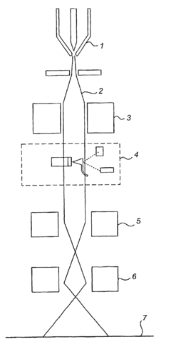
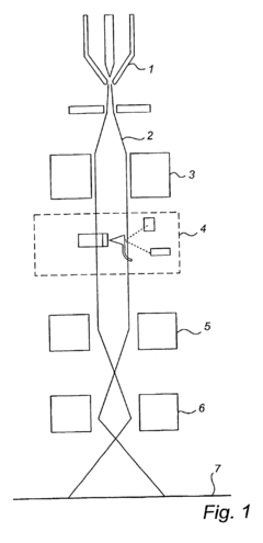
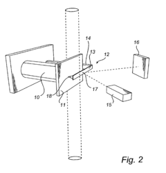
Method for increasing the measurement information available from a transmission electron microscope and a transmission electron microscopy device
PatentInactiveUS6864483B2
Innovation
- Integration of an atomic force microscopy (AFM) device within a transmission electron microscope (TEM) enables simultaneous TEM and AFM measurements, allowing for the investigation of force interactions and geometry of interacting particles by measuring cantilever deflection using an electron beam or strain-sensitive devices.
Fabrication of patterned and ordered nanoparticles
PatentInactiveEP2179441A1
Innovation
- A novel technique using charged nanoparticles that are deposited in a random pattern on a surface and then reordered using controlled fields, such as an atomic force microscope (AFM) or electron beam, to create large arrays of uniformly spaced nanoparticles with high size uniformity, enabling cost-effective mass production compatible with silicon CMOS technology.
Sample Preparation Techniques and Limitations
Sample preparation represents a critical differentiating factor between Atomic Force Microscopy (AFM) and Transmission Electron Microscopy (TEM), significantly impacting their respective applications across scientific and industrial domains. AFM sample preparation is notably less demanding, requiring minimal processing as specimens need only be mounted on a flat substrate. This simplicity allows for the examination of samples in their near-native state, preserving delicate structures and enabling in-situ studies of biological specimens in physiological environments—a substantial advantage for life science applications.
In contrast, TEM demands extensive and often destructive sample preparation. Specimens must be exceptionally thin (typically 50-100 nm) to allow electron transmission, necessitating techniques such as ultramicrotomy, ion milling, or focused ion beam (FIB) sectioning. These processes frequently introduce artifacts and can alter the sample's original structure, potentially compromising the validity of observations, particularly in sensitive biological materials.
Environmental constraints further distinguish these technologies. AFM can operate in various environments including ambient conditions, liquids, and controlled atmospheres, facilitating dynamic studies of processes like protein folding or cellular responses. TEM, however, requires high vacuum conditions that preclude the examination of hydrated specimens without specialized cryo-preparation techniques, limiting its application for certain biological investigations.
Resolution limitations are intrinsically linked to sample preparation methods. While TEM achieves superior atomic-scale resolution, this advantage comes at the cost of complex preparation protocols that may introduce structural alterations. AFM offers nanometer-scale resolution with minimal sample disruption, making it preferable for applications where preserving native structures outweighs the need for atomic-level detail.
Time considerations also factor significantly into technology selection. AFM sample preparation can be completed within minutes, enabling rapid analysis and higher throughput. TEM preparation may require hours or days, creating bottlenecks in research workflows and limiting its suitability for time-sensitive applications or large-scale studies.
Cost implications of sample preparation extend beyond time investment. TEM preparation requires specialized equipment and consumables, including heavy metal stains, embedding resins, and precision thinning apparatus. AFM preparation typically demands fewer resources, making it more accessible for facilities with limited budgets or for routine analytical applications where operational efficiency is paramount.
Cost-Benefit Analysis and ROI Considerations
When evaluating the implementation of Atomic Force Microscopy (AFM) versus Transmission Electron Microscopy (TEM) technologies, a comprehensive cost-benefit analysis is essential for organizations to make informed investment decisions. The initial acquisition costs present a significant contrast: AFM systems typically range from $100,000 to $500,000, while TEM installations can exceed $1-5 million due to their complex electron optics, vacuum systems, and specialized housing requirements.
Operational expenses further differentiate these technologies. AFM offers lower running costs with minimal sample preparation requirements and reduced energy consumption. Conversely, TEM demands substantial ongoing investment in specialized sample preparation equipment, highly trained operators, and significantly higher energy usage due to electron acceleration requirements. Additionally, TEM facilities often require dedicated infrastructure modifications, including vibration isolation and electromagnetic shielding.
Maintenance considerations reveal that AFM systems generally require annual service contracts of approximately 5-10% of the initial purchase price, while TEM maintenance can reach 10-15% of the acquisition cost. The lifespan of AFM components typically extends 5-7 years before major upgrades are necessary, whereas TEM systems may require substantial component replacements within similar timeframes despite their longer overall operational life.
Return on investment calculations must account for research output potential and application versatility. AFM demonstrates superior ROI in materials science, polymer research, and biological applications where surface characterization is paramount. Its non-destructive nature allows for sample preservation and repeated analysis, enhancing long-term value. TEM offers exceptional ROI in semiconductor research, nanotechnology, and structural biology where atomic-level internal structure visualization justifies the higher investment.
Productivity metrics indicate that AFM can process 10-15 samples daily with minimal preparation time, while TEM throughput is limited to 3-5 samples due to extensive preparation requirements. However, the depth and quality of TEM data often compensate for this reduced throughput in specialized applications requiring atomic-resolution imaging.
Organizations should consider scalability factors in their investment strategy. AFM technology allows for modular upgrades and accessories that can extend capabilities incrementally, whereas TEM typically requires substantial one-time investments with limited modularity. This difference significantly impacts budget planning and resource allocation strategies, particularly for growing research facilities with evolving needs.
Unlock deeper insights with Patsnap Eureka Quick Research — get a full tech report to explore trends and direct your research. Try now!
Generate Your Research Report Instantly with AI Agent
Supercharge your innovation with Patsnap Eureka AI Agent Platform!