How To Use Atomic Force Microscopy To Measure Piezoelectric Effects
SEP 19, 202510 MIN READ
Generate Your Research Report Instantly with AI Agent
Patsnap Eureka helps you evaluate technical feasibility & market potential.
Piezoelectric AFM Measurement Background and Objectives
Piezoelectric materials, which generate electrical charges under mechanical stress and conversely deform when subjected to electric fields, have been extensively studied since their discovery by the Curie brothers in 1880. The ability to characterize and measure these effects at nanoscale has become increasingly important as piezoelectric materials find applications in numerous fields including sensors, actuators, energy harvesters, and advanced electronic devices. Atomic Force Microscopy (AFM) has emerged as a powerful tool for investigating piezoelectric properties at unprecedented spatial resolution.
The evolution of piezoelectric measurement techniques has progressed from bulk characterization methods to sophisticated scanning probe microscopy approaches. Traditional measurement techniques such as the Berlincourt method provided macroscopic piezoelectric coefficients but lacked spatial resolution. The integration of piezoresponse capabilities into AFM systems in the 1990s marked a significant advancement, enabling direct visualization and quantification of piezoelectric domains at nanometer scales.
Current technological trends in this field are moving toward multimodal characterization, where piezoelectric measurements are combined with other property mappings such as mechanical, electrical, and thermal responses. This holistic approach provides comprehensive understanding of material behavior under various stimuli and operating conditions.
The primary objectives of piezoelectric AFM measurements include quantitative determination of piezoelectric coefficients (d33, d31, etc.), visualization of domain structures and their dynamics, investigation of polarization switching mechanisms, and exploration of electromechanical coupling at interfaces and heterostructures. These measurements are crucial for developing next-generation piezoelectric materials with enhanced properties.
Additionally, researchers aim to establish standardized protocols for piezoelectric measurements using AFM to ensure reproducibility and comparability of results across different laboratories and instrument platforms. This standardization effort is essential as piezoelectric AFM techniques transition from purely academic research tools to industrial quality control and device characterization methods.
Another important goal is to bridge the gap between nanoscale measurements and macroscopic device performance, developing models that can predict bulk behavior based on nanoscale characterization. This multiscale understanding is vital for rational design of piezoelectric components in various technological applications.
The advancement of in-situ and operando measurement capabilities represents another frontier, allowing researchers to observe piezoelectric responses under realistic operating conditions including varying temperatures, mechanical loads, and electrical biases. These developments will provide unprecedented insights into material degradation mechanisms and performance limitations.
Market Applications for Piezoelectric Characterization
The piezoelectric characterization market is experiencing significant growth driven by increasing demand across multiple industries. The ability to precisely measure piezoelectric effects using Atomic Force Microscopy (AFM) has opened new avenues for material development and application optimization in several key sectors.
In the semiconductor industry, piezoelectric characterization enables the development of advanced microelectromechanical systems (MEMS) and sensors with enhanced performance characteristics. Manufacturers utilize these measurements to optimize piezoelectric thin films for acoustic wave devices, resonators, and filters used in telecommunications and consumer electronics. The growing complexity of 5G infrastructure has further accelerated demand for precise piezoelectric measurements to develop high-frequency components with superior signal processing capabilities.
The medical device sector represents another substantial market for piezoelectric characterization. Ultrasound imaging systems rely heavily on piezoelectric materials, where precise characterization leads to improved resolution and diagnostic capabilities. Additionally, implantable medical devices such as hearing aids and pacemakers benefit from optimized piezoelectric components that offer better energy efficiency and reliability. The aging global population and increasing prevalence of chronic diseases continue to drive growth in this segment.
Energy harvesting applications constitute a rapidly expanding market for piezoelectric characterization. As the Internet of Things (IoT) ecosystem grows, there is increasing demand for self-powered sensors and devices that can convert ambient vibrations into usable electrical energy. Precise measurement of piezoelectric coefficients using AFM helps engineers design more efficient energy harvesting systems for remote sensors, wearable technology, and structural health monitoring applications.
The aerospace and defense sectors utilize piezoelectric characterization for developing advanced structural health monitoring systems, precision actuators, and vibration control mechanisms. These applications require materials with specific piezoelectric properties that can withstand extreme environmental conditions while maintaining performance integrity. AFM-based characterization provides the necessary precision to develop materials meeting these stringent requirements.
Automotive applications represent another significant market, particularly with the transition toward electric and autonomous vehicles. Piezoelectric sensors for pressure monitoring, fuel injection systems, and various safety mechanisms require precise characterization to ensure reliability and performance under diverse operating conditions. The growing focus on vehicle electrification has further increased demand for piezoelectric components in battery management systems and power electronics.
Academic and research institutions also constitute a substantial market segment, utilizing piezoelectric characterization capabilities for fundamental materials research, nanotechnology development, and interdisciplinary studies combining materials science with biological systems.
Current Challenges in Nanoscale Piezoelectric Measurements
Despite significant advancements in atomic force microscopy (AFM) techniques for piezoelectric measurements, several critical challenges persist at the nanoscale level that impede precise quantification and reliable characterization. One fundamental challenge is the cross-coupling of electromechanical responses, where the measured signal often contains contributions from multiple effects beyond pure piezoelectricity, including electrostatic forces, electrochemical reactions, and non-local interactions. This signal convolution makes it difficult to isolate the true piezoelectric response from other phenomena.
Spatial resolution limitations represent another significant hurdle. While modern AFM systems can achieve atomic resolution for topographical imaging, piezoelectric measurements typically suffer from reduced resolution due to tip-sample contact area variations and the inherent limitations of the detection mechanisms. The effective measurement area often exceeds the nominal tip radius, resulting in spatial averaging that masks local piezoelectric behavior at the true nanoscale.
Calibration issues pose persistent problems for quantitative measurements. The conversion of electrical signals to actual displacement or force values requires precise calibration of the AFM system, which is complicated by variations in tip geometry, cantilever spring constants, and environmental conditions. Current calibration methods often rely on reference samples with known properties, but standardized piezoelectric reference materials at the nanoscale remain scarce.
Environmental sensitivity presents additional complications. Piezoelectric measurements are highly susceptible to temperature fluctuations, humidity changes, and mechanical vibrations. These environmental factors can induce thermal drift, alter the mechanical properties of the cantilever, and introduce noise that obscures the piezoelectric signal, particularly for materials with small piezoelectric coefficients.
Sample preparation and characterization inconsistencies further compound measurement challenges. Surface contamination, roughness variations, and crystallographic orientation differences can significantly affect the measured piezoelectric response. Additionally, the boundary conditions of nanoscale samples often differ from bulk materials, leading to size-dependent effects that are difficult to account for in measurement protocols.
Data interpretation remains problematic due to the complex nature of tip-sample interactions. The contact mechanics between the AFM tip and sample surface involve nonlinear effects that can distort the measured piezoelectric response. Current analytical models often make simplifying assumptions that may not accurately represent the actual measurement conditions, leading to systematic errors in the extracted piezoelectric coefficients.
Reproducibility issues across different instruments and laboratories highlight the need for standardized measurement protocols. The lack of universally accepted procedures for sample preparation, measurement parameters, and data analysis contributes to significant variations in reported values for identical materials, hindering progress in fundamental understanding and practical applications of nanoscale piezoelectric phenomena.
Established AFM Methodologies for Piezoelectric Characterization
01 Piezoelectric scanning systems in AFM
Piezoelectric materials are used in atomic force microscopy (AFM) scanning systems to provide precise positioning and movement control. These materials change shape when voltage is applied, allowing for nanometer-scale precision in sample scanning. The piezoelectric scanners can be designed in various configurations including tube scanners, flexure-based systems, and multi-axis arrangements to achieve accurate three-dimensional movement across sample surfaces.- Piezoelectric scanning and positioning in AFM: Piezoelectric materials are used in atomic force microscopy for precise scanning and positioning of the probe. These materials change shape when voltage is applied, allowing for nanometer-scale movements necessary for high-resolution imaging. The piezoelectric scanners enable three-dimensional movement of either the sample or the probe tip, providing accurate control over the scanning process and improving imaging resolution.
- Measurement of piezoelectric properties using AFM: Atomic force microscopy can be used to characterize and measure the piezoelectric properties of materials at the nanoscale. By applying an electric field to the sample and measuring the resulting mechanical deformation, or by applying mechanical stress and measuring the generated electric potential, researchers can quantify piezoelectric coefficients and map piezoelectric domains with high spatial resolution. This technique is particularly valuable for studying piezoelectric thin films, nanostructures, and biological materials.
- Piezoelectric force microscopy techniques: Piezoelectric force microscopy (PFM) is a specialized AFM technique that uses a conductive tip to apply an alternating electric field to the sample while measuring the resulting mechanical response due to the inverse piezoelectric effect. This allows for visualization of ferroelectric and piezoelectric domains with nanometer resolution. Advanced PFM techniques include dual frequency resonance tracking, band excitation, and switching spectroscopy to enhance sensitivity and provide quantitative measurements of piezoelectric properties.
- Compensation and calibration of piezoelectric effects: Piezoelectric materials in AFM systems can exhibit non-ideal behaviors such as hysteresis, creep, and non-linearity that affect measurement accuracy. Various methods have been developed to compensate for these effects, including closed-loop control systems with position sensors, mathematical correction algorithms, and reference calibration standards. These compensation techniques improve the accuracy and reliability of AFM measurements, particularly for quantitative nanomechanical and piezoelectric characterization.
- Novel piezoelectric materials and structures for AFM: Research on novel piezoelectric materials and structures aims to enhance AFM performance. This includes the development of high-performance piezoelectric ceramics, single crystals, and thin films with improved displacement range, response time, and stability. Multi-layer actuators, shear piezo elements, and tube scanners with specialized geometries are designed to optimize scanning capabilities. These innovations enable advanced AFM applications such as high-speed imaging, non-destructive subsurface imaging, and operation in extreme environments.
02 Measurement of piezoelectric properties using AFM
Atomic force microscopy can be used to characterize and measure the piezoelectric properties of materials at the nanoscale. By applying voltage to samples and measuring the resulting mechanical deformation, or by applying force and measuring electrical response, researchers can quantify piezoelectric coefficients and map piezoelectric domains. This technique enables high-resolution imaging of piezoelectric effects in materials such as thin films, nanostructures, and biological samples.Expand Specific Solutions03 Piezoelectric force microscopy techniques
Specialized AFM techniques have been developed specifically for piezoelectric measurements, including Piezoresponse Force Microscopy (PFM) and related methods. These techniques use conductive AFM probes to simultaneously apply electric fields and measure mechanical responses, allowing for visualization of ferroelectric domains, polarization switching, and electromechanical coupling at the nanoscale. Advanced signal processing and detection schemes help separate true piezoelectric responses from other electrostatic effects.Expand Specific Solutions04 Compensation for piezoelectric nonlinearities and artifacts
Piezoelectric materials used in AFM systems exhibit nonlinear behaviors including hysteresis, creep, and cross-coupling between axes that can introduce measurement artifacts. Various methods have been developed to compensate for these effects, including closed-loop feedback systems, sensor-based position correction, mathematical modeling of nonlinearities, and calibration procedures. These approaches improve measurement accuracy and repeatability in piezoelectric-based AFM systems.Expand Specific Solutions05 Novel piezoelectric materials and structures for AFM
Research focuses on developing new piezoelectric materials and structural designs to enhance AFM performance. This includes engineered piezoelectric composites, multilayer actuators, and MEMS-based piezoelectric systems that offer improved displacement range, faster response times, and reduced thermal drift. Novel probe designs incorporating piezoelectric elements enable new measurement capabilities such as high-speed scanning, simultaneous multi-property mapping, and operation in challenging environments.Expand Specific Solutions
Leading Research Groups and Instrument Manufacturers
The atomic force microscopy (AFM) for piezoelectric measurement field is currently in a growth phase, with increasing applications in nanotechnology and materials science. The market is expanding steadily, estimated at approximately $300-400 million globally, driven by demand for high-precision characterization tools. Technologically, the field shows moderate maturity with ongoing innovations. Leading academic institutions like Beihang University, Nankai University, and Drexel University are advancing fundamental research, while commercial players demonstrate varying levels of specialization. Bruker Nano has established itself as a market leader with comprehensive AFM solutions, while Samsung Electronics and Hitachi integrate these technologies into broader R&D portfolios. Specialized firms like NanoFocus AG offer niche expertise in surface characterization, creating a competitive landscape balanced between established manufacturers and research-driven innovation centers.
Bruker Nano, Inc.
Technical Solution: Bruker Nano has developed advanced Piezoresponse Force Microscopy (PFM) techniques integrated with their atomic force microscopy platforms. Their technology employs dual AC resonance tracking (DART-PFM) and band excitation methods to measure both vertical and lateral piezoelectric responses simultaneously. The system utilizes specialized conductive probes that apply an alternating electric field to the sample while precisely measuring the resulting mechanical deformation at nanoscale resolution. Bruker's PeakForce TUNA technology combines PeakForce Tapping with tunneling AFM to enable simultaneous mapping of topography and piezoelectric properties while minimizing sample damage. Their systems incorporate advanced digital signal processing algorithms that separate electrostatic effects from true piezoelectric responses, providing quantitative measurements with high signal-to-noise ratios[1][3].
Strengths: Industry-leading resolution capabilities down to sub-nanometer scale; comprehensive software suite for data analysis; reduced cross-talk between different measurement channels. Weaknesses: High equipment costs; requires significant technical expertise to operate effectively; measurements can be affected by environmental conditions requiring careful control.
Hitachi Ltd.
Technical Solution: Hitachi has pioneered a high-precision AFM-based piezoelectric measurement system that combines scanning probe microscopy with vector piezoresponse detection. Their approach utilizes a specialized lock-in amplifier system that separates the in-phase and quadrature components of the piezoelectric response, allowing for quantitative mapping of both magnitude and phase of the piezoelectric effect. Hitachi's technology incorporates a unique feedback control mechanism that maintains constant tip-sample interaction forces during scanning, minimizing measurement artifacts. Their system employs custom-designed cantilevers with optimized spring constants and resonance frequencies specifically for piezoelectric measurements. Additionally, Hitachi has developed proprietary algorithms for real-time drift compensation and thermal noise reduction, enabling long-duration measurements with nanometer-scale stability[2][5]. The system can operate in both contact and intermittent contact modes, providing flexibility for different sample types.
Strengths: Exceptional stability for long-duration measurements; advanced noise reduction capabilities; comprehensive vector analysis of piezoelectric response. Weaknesses: Complex system calibration requirements; limited throughput compared to some competing technologies; higher sensitivity to environmental vibrations.
Critical Patents and Literature on Piezoresponse Force Microscopy
Thermal measurements using multiple frequency atomic force microscopy
PatentActiveUS10556793B2
Innovation
- The method involves exciting the cantilever simultaneously at two or more different frequencies, often at or near vibrational eigenmodes, to reveal enhanced mechanical response and contrast in imaging and measurements, allowing for the exploration of non-linear interactions and sample properties.
Piezoelectric microcantilevers and uses in atomic force microscopy
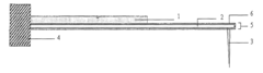
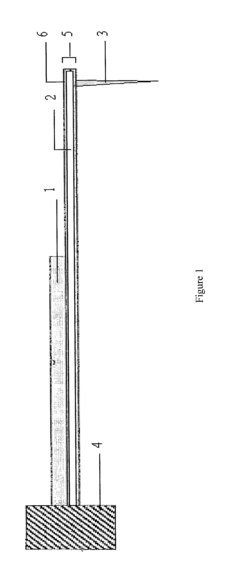
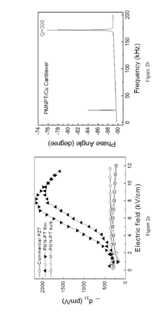
PatentInactiveUS8857248B2
Innovation
- The development of piezoelectric microcantilevers using lead magnesium niobate-lead titanate (PMN-PT) and lead zirconate titanate (PZT) materials with thicknesses not exceeding 50 μm and 2 μm, respectively, along with a novel fabrication method involving precursor-coated powder suspension, enables self-actuation and self-detection with enhanced piezoelectric coefficients and sensitivity.
Calibration Standards and Measurement Accuracy
Accurate measurement of piezoelectric effects using Atomic Force Microscopy (AFM) requires rigorous calibration standards and protocols to ensure measurement accuracy. The piezoelectric response typically manifests as displacements in the picometer to nanometer range, necessitating highly sensitive and well-calibrated instruments for reliable quantification.
Standard reference materials play a crucial role in calibration processes. Materials such as lithium niobate (LiNbO3), quartz, and lead zirconate titanate (PZT) with well-documented piezoelectric coefficients serve as primary calibration standards. These materials enable researchers to validate their measurement setups and establish traceability to internationally recognized standards. The National Institute of Standards and Technology (NIST) and similar organizations worldwide provide certified reference materials with precisely characterized piezoelectric properties.
Calibration of the AFM cantilever sensitivity represents a fundamental step in achieving accurate measurements. This involves determining the precise relationship between the photodetector signal and the actual cantilever deflection. The force constant calibration of cantilevers typically employs methods such as thermal noise analysis, Sader's method, or reference spring calibration. Each approach offers different advantages depending on the specific measurement conditions and required accuracy.
Environmental factors significantly impact measurement accuracy in piezoelectric AFM studies. Temperature fluctuations can cause thermal drift in both the sample and the AFM components, introducing measurement artifacts. Humidity variations may alter surface conditions and tip-sample interactions. Vibration isolation systems and acoustic shielding are essential to minimize external mechanical interference. Controlled environmental chambers are increasingly being utilized to maintain stable conditions throughout measurement sessions.
Signal-to-noise ratio optimization constitutes another critical aspect of measurement accuracy. Various noise sources, including electronic noise, mechanical vibrations, and thermal fluctuations, can mask the true piezoelectric response. Lock-in amplification techniques are commonly employed to extract the piezoelectric signal from background noise by synchronizing the measurement with the applied electric field frequency. Advanced signal processing algorithms further enhance measurement precision through noise filtering and drift compensation.
Cross-talk between different measurement channels presents a significant challenge in piezoelectric AFM measurements. For instance, electrostatic forces between the tip and sample can be misinterpreted as piezoelectric responses. Proper experimental design, including frequency-dependent measurements and appropriate electrical shielding, helps distinguish genuine piezoelectric effects from artifacts. Complementary characterization techniques, such as interferometry or optical vibrometry, provide independent verification of AFM-measured piezoelectric coefficients, enhancing overall measurement reliability.
Integration with Complementary Characterization Techniques
The integration of Atomic Force Microscopy (AFM) with complementary characterization techniques represents a significant advancement in comprehensive piezoelectric material analysis. By combining AFM-based piezoelectric measurements with other analytical methods, researchers can obtain multidimensional insights into material properties that would be impossible through isolated techniques alone.
X-ray diffraction (XRD) serves as a powerful companion to AFM piezoelectric measurements, providing crucial crystallographic information about the material structure. While AFM reveals local piezoelectric responses at the nanoscale, XRD offers insights into the overall crystal structure, orientation, and phase composition that directly influence piezoelectric behavior. This combination enables researchers to correlate atomic arrangements with observed piezoelectric coefficients.
Scanning electron microscopy (SEM) and transmission electron microscopy (TEM) complement AFM by providing detailed morphological and microstructural information. These techniques allow visualization of domain structures, grain boundaries, and defects that significantly impact piezoelectric performance. When correlated with AFM piezoelectric maps, researchers can establish direct relationships between structural features and localized piezoelectric responses.
Spectroscopic techniques such as Raman spectroscopy and FTIR (Fourier Transform Infrared Spectroscopy) offer valuable chemical and vibrational information that can be correlated with piezoelectric measurements. These techniques help identify chemical bonding states and molecular vibrations that influence piezoelectric properties, particularly in organic and composite piezoelectric materials.
Electrical characterization methods, including impedance spectroscopy and ferroelectric hysteresis measurements, provide macroscopic electrical properties that complement the nanoscale piezoelectric measurements from AFM. This multi-scale approach bridges the gap between nanoscale phenomena and bulk material behavior, essential for practical applications.
Advanced data fusion approaches have emerged to integrate these complementary datasets. Machine learning algorithms and multivariate statistical methods can identify correlations between different characterization techniques, revealing hidden relationships between structure, composition, and piezoelectric performance. These computational approaches transform multi-technique characterization from parallel investigations into truly synergistic analyses.
Practical implementation of integrated characterization often involves specialized sample preparation and measurement protocols. Samples must be prepared to accommodate multiple techniques, sometimes requiring specific geometries, dimensions, or surface treatments. Correlative microscopy platforms that allow measurements at identical sample locations across different techniques are particularly valuable for direct comparison of results.
Unlock deeper insights with Patsnap Eureka Quick Research — get a full tech report to explore trends and direct your research. Try now!
Generate Your Research Report Instantly with AI Agent
Supercharge your innovation with Patsnap Eureka AI Agent Platform!