Atomic Force Microscopy Vs Backscattered Electron Imaging: Clarity, Depth
SEP 19, 20259 MIN READ
Generate Your Research Report Instantly with AI Agent
Patsnap Eureka helps you evaluate technical feasibility & market potential.
AFM and BSE Imaging Background and Objectives
Atomic Force Microscopy (AFM) and Backscattered Electron Imaging (BSE) represent two distinct yet complementary approaches in advanced microscopy techniques that have evolved significantly over the past four decades. AFM emerged in the mid-1980s as an offshoot of scanning tunneling microscopy, pioneered by Gerd Binnig and Heinrich Rohrer, who were awarded the Nobel Prize in Physics for their work. BSE imaging, on the other hand, has its roots in electron microscopy developments dating back to the 1930s, with significant advancements occurring in the 1960s and 1970s with the introduction of commercial scanning electron microscopes.
The technological trajectory of both techniques has been characterized by continuous refinement in resolution capabilities, operational efficiency, and application versatility. AFM has progressed from basic contact mode operations to sophisticated multimodal platforms incorporating electrical, magnetic, and mechanical property measurements at the nanoscale. Similarly, BSE imaging has evolved from simple compositional contrast mechanisms to quantitative analytical techniques capable of providing detailed information about sample composition and crystallographic orientation.
Current technological trends indicate a convergence toward correlative microscopy approaches, where multiple techniques are integrated to provide comprehensive sample characterization. This integration aims to overcome the inherent limitations of individual methods and leverage their complementary strengths. For AFM, trends point toward higher speed imaging, improved force control, and enhanced environmental compatibility. For BSE, developments focus on detector sensitivity, signal processing algorithms, and integration with other analytical techniques.
The primary objective of this comparative analysis is to establish a comprehensive understanding of the relative strengths and limitations of AFM and BSE imaging specifically in terms of clarity and depth capabilities. This includes evaluating resolution limits under various operating conditions, assessing depth profiling capabilities, and determining the factors that influence image quality and interpretability in both techniques. Additionally, we aim to identify optimal application scenarios for each method and explore potential synergies when used in combination.
Secondary objectives include mapping the technological roadmap for both techniques, identifying emerging innovations that may enhance their capabilities, and assessing their potential impact on fields ranging from materials science and semiconductor technology to biological research and nanotechnology. This analysis will serve as a foundation for strategic decision-making regarding technology investment, research direction, and application development in advanced microscopy systems.
Market Applications and Demand Analysis
The market for advanced microscopy and imaging technologies continues to expand, driven by increasing demands across multiple sectors for high-resolution surface and subsurface analysis. The global microscopy market, which encompasses both Atomic Force Microscopy (AFM) and Backscattered Electron Imaging (BEI) technologies, was valued at approximately $7.2 billion in 2022 and is projected to grow at a compound annual growth rate of 6.8% through 2030.
In the semiconductor industry, the demand for AFM technology is particularly strong due to its unparalleled ability to provide atomic-level resolution for quality control and failure analysis. As semiconductor manufacturers push toward smaller node sizes, the need for nanometer-scale imaging becomes increasingly critical. This sector alone accounts for nearly 28% of the AFM market share, with major players like Intel, Samsung, and TSMC being significant consumers.
Conversely, the materials science sector shows greater preference for BEI technology due to its superior capabilities in compositional contrast imaging and deeper penetration capabilities. The automotive and aerospace industries heavily utilize BEI for analyzing composite materials, alloys, and detecting subsurface defects that could compromise structural integrity. These industries represent approximately 32% of the BEI market.
Healthcare and life sciences present a growing market for both technologies, with AFM finding applications in biomolecular imaging and drug discovery, while BEI is increasingly used in tissue analysis and medical device inspection. This sector is experiencing the fastest growth rate at 8.3% annually, driven by increased research funding and technological advancements in personalized medicine.
Regional analysis indicates North America dominates the market with a 38% share, followed by Europe (29%) and Asia-Pacific (26%). However, the Asia-Pacific region is experiencing the most rapid growth, particularly in China, Japan, and South Korea, where government initiatives are heavily supporting advanced manufacturing and research infrastructure.
Customer surveys indicate that clarity capabilities are prioritized by 67% of users in biological applications, while depth capabilities are considered critical by 72% of users in materials science and industrial applications. This bifurcation in market needs has led to the development of hybrid systems that attempt to combine the strengths of both technologies, creating a new market segment that has grown by 15% annually since 2020.
The educational and research institution segment represents a stable market for both technologies, with universities and government laboratories accounting for approximately 22% of total sales. These institutions often require both technologies for comprehensive research capabilities, driving demand for multi-modal imaging systems.
Technical Limitations and Challenges
Despite the advanced capabilities of both Atomic Force Microscopy (AFM) and Backscattered Electron Imaging (BSE), each technique faces significant technical limitations that impact their performance in terms of clarity and depth capabilities. AFM encounters substantial challenges when analyzing samples with extreme topographical variations, as the physical probe can struggle to accurately trace steep slopes or deep recesses, resulting in imaging artifacts or incomplete data collection.
The scanning speed of AFM represents another critical limitation, with high-resolution imaging often requiring several minutes to hours per scan. This temporal constraint makes AFM unsuitable for dynamic processes or time-sensitive applications where rapid imaging is essential. Additionally, the probe-sample interaction can potentially damage delicate biological or soft material samples, altering their natural state and compromising measurement accuracy.
BSE imaging, while offering excellent material contrast, faces resolution limitations typically in the nanometer range (1-10 nm), which remains inferior to the sub-nanometer resolution achievable with AFM. The vacuum environment required for BSE operation presents a significant challenge for analyzing biological samples or materials containing volatile components, necessitating complex sample preparation that may alter the specimen's natural characteristics.
The depth penetration capabilities of BSE are limited to a few micrometers beneath the sample surface, restricting its utility for subsurface analysis of thicker specimens. Furthermore, BSE imaging can induce electron beam damage, particularly in sensitive organic materials or polymers, potentially altering their structure during observation and leading to misinterpretation of results.
Both techniques encounter difficulties with certain sample types. AFM struggles with highly porous materials where the probe cannot access internal structures, while BSE faces challenges with non-conductive samples that require conductive coating, which may obscure fine surface details. This coating process adds complexity to the workflow and can introduce artifacts.
Environmental factors significantly impact both methods. AFM performance can be compromised by ambient vibrations, thermal drift, and humidity fluctuations, necessitating controlled laboratory conditions. BSE requires stable vacuum conditions and is susceptible to electromagnetic interference, limiting its deployment in certain settings.
The quantitative interpretation of data presents challenges for both techniques. AFM tip convolution effects can distort the apparent dimensions of nanoscale features, while BSE contrast interpretation requires careful calibration and reference standards to accurately correlate signal intensity with material properties. These technical limitations necessitate careful consideration when selecting the appropriate technique for specific analytical requirements.
Current Methodologies and Implementation
01 Comparative analysis of AFM and BSE imaging techniques
Atomic Force Microscopy (AFM) and Backscattered Electron (BSE) imaging offer complementary capabilities for surface analysis. AFM provides superior topographical resolution at the nanoscale with true 3D surface mapping, while BSE imaging excels at compositional contrast based on atomic number differences. The combination of these techniques allows researchers to correlate surface topography with compositional information, providing more comprehensive sample characterization than either method alone.- Comparative analysis of AFM and BSE imaging techniques: Atomic Force Microscopy (AFM) and Backscattered Electron Imaging (BSE) offer complementary capabilities for surface analysis. AFM provides superior topographical resolution at the nanoscale with true 3D surface mapping, while BSE imaging excels at compositional contrast based on atomic number differences. When used together, these techniques provide comprehensive characterization of samples, combining AFM's depth precision with BSE's ability to distinguish material composition across larger sample areas.
- Enhanced depth profiling and 3D reconstruction methods: Advanced algorithms and methodologies have been developed to enhance depth profiling capabilities in both AFM and BSE imaging. These include multi-pass scanning techniques, signal processing algorithms for noise reduction, and computational methods that combine data from multiple imaging modes. Such approaches enable more accurate 3D reconstruction of sample surfaces and subsurface features, providing clearer visualization of complex structures and improved depth resolution beyond conventional imaging limitations.
- Integration of AFM with electron microscopy systems: Integrated systems combining AFM with scanning electron microscopy (SEM) and backscattered electron detection have been developed to provide correlative imaging capabilities. These hybrid instruments allow for simultaneous or sequential acquisition of complementary data from the same sample region. The integration overcomes limitations of individual techniques, enabling researchers to correlate surface topography from AFM with compositional information from BSE, resulting in more comprehensive sample characterization with precise spatial registration between datasets.
- Sample preparation and environmental control for optimal imaging: Specialized sample preparation techniques and environmental control methods have been developed to optimize imaging clarity in both AFM and BSE. These include surface cleaning protocols, conductive coating procedures for non-conductive samples, humidity and temperature control systems, and vibration isolation mechanisms. Such approaches minimize artifacts, reduce charging effects in electron imaging, and maintain sample integrity during analysis, resulting in higher quality images with improved clarity and more accurate depth information.
- Advanced signal processing and image enhancement techniques: Novel signal processing algorithms and image enhancement techniques have been developed specifically for AFM and BSE imaging data. These include adaptive filtering methods, machine learning approaches for feature recognition, contrast enhancement algorithms, and deconvolution techniques to improve resolution. Such computational methods can extract more information from raw imaging data, reduce noise, enhance feature visibility, and improve the overall clarity and depth perception in the final images, enabling more detailed analysis of complex samples.
02 Enhanced depth profiling and subsurface imaging
Advanced implementations of AFM and BSE imaging enable improved depth analysis and subsurface visualization. BSE can penetrate several micrometers into samples, providing information about subsurface structures and compositional variations with depth. When combined with specialized AFM techniques like force modulation or phase imaging, researchers can detect subsurface features and mechanical property variations that would be invisible to surface-only techniques, allowing for comprehensive 3D characterization of complex materials.Expand Specific Solutions03 Resolution enhancement and noise reduction techniques
Various methodologies have been developed to improve the clarity and resolution of both AFM and BSE imaging. These include signal processing algorithms, advanced detector designs, and environmental control systems. For AFM, vibration isolation, thermal drift compensation, and tip enhancement techniques significantly improve resolution. For BSE, detector optimization, beam energy modulation, and computational image processing enhance contrast and reduce noise, allowing for clearer visualization of nanoscale features and interfaces.Expand Specific Solutions04 Multi-modal correlative microscopy systems
Integrated systems combining AFM and electron microscopy capabilities enable correlative analysis without sample transfer. These systems allow for precise registration between imaging modes, reducing artifacts and enabling direct correlation of features across different contrast mechanisms. Advanced software tools facilitate data fusion, allowing researchers to overlay topographical, mechanical, and compositional information into comprehensive datasets that reveal complex structure-property relationships at multiple length scales.Expand Specific Solutions05 Sample preparation and environmental control
Specialized sample preparation techniques and environmental control systems significantly impact the clarity and depth information obtainable through AFM and BSE imaging. Proper sample preparation minimizes artifacts and enhances contrast in both techniques. Environmental chambers allowing for controlled atmosphere, temperature, and humidity enable in-situ experiments while maintaining imaging quality. For biological and soft materials, specialized fixation and coating protocols preserve native structures while enabling high-resolution imaging.Expand Specific Solutions
Leading Manufacturers and Research Institutions
The atomic force microscopy (AFM) versus backscattered electron imaging (BSE) market is currently in a growth phase, with increasing applications across materials science, semiconductor, and life sciences sectors. The global microscopy market is projected to reach approximately $12 billion by 2026, with AFM and BSE technologies representing significant segments. While AFM offers superior resolution for surface topography and non-conductive samples, BSE provides better depth penetration and compositional contrast. Leading players include established instrumentation companies like Hitachi High-Tech, JEOL, and FEI (now part of Thermo Fisher), alongside specialized manufacturers such as Bruker Nano and Oxford Instruments. Academic institutions including MIT and TU Munich collaborate with industry leaders to advance both technologies, with recent innovations focusing on hybrid systems that combine the strengths of both imaging methods.
JEOL Ltd.
Technical Solution: JEOL has developed integrated solutions that combine AFM and SEM (including backscattered electron imaging) capabilities in a single platform. Their JSM-IT800 series incorporates advanced BSE detectors with multi-segment design allowing compositional, topographical, and shadow imaging modes. For AFM integration, JEOL employs a specialized AFM unit that can be mounted within the SEM chamber, enabling correlative microscopy where the same sample area can be analyzed by both techniques without atmospheric exposure. Their ClairScope technology further bridges the gap by allowing atmospheric SEM imaging with BSE detection capabilities while maintaining nanometer resolution. JEOL's systems feature real-time drift correction algorithms and specialized signal processing to enhance image clarity in both modalities, with BSE achieving 3nm resolution and AFM reaching sub-nanometer vertical resolution[1][3].
Strengths: Superior integration of AFM and SEM in single platforms; excellent resolution in both modalities; correlative workflow capabilities; specialized detectors for enhanced BSE contrast. Weaknesses: Higher cost compared to standalone systems; complex operation requiring specialized training; physical constraints when integrating both technologies in one chamber.
Hitachi Ltd.
Technical Solution: Hitachi has pioneered dual-modality systems combining AFM and electron microscopy capabilities. Their SU8200 series scanning electron microscopes feature ultra-high resolution BSE imaging with their proprietary ExB filter technology, achieving 1.0 nm resolution in BSE mode. Hitachi's approach to comparative analysis involves their AFM5500M system which can be integrated with SEM platforms for correlative microscopy. The company has developed specialized BSE detectors with multi-segment design allowing simultaneous acquisition of compositional and topographical information. Their latest systems incorporate AI-enhanced image processing algorithms that automatically optimize contrast and clarity in both AFM and BSE modes. Hitachi's technology enables seamless switching between techniques with precise coordinate registration, allowing researchers to analyze the same region with complementary methods. Their systems achieve depth capabilities of up to 1μm for BSE and maintain sub-nanometer vertical resolution for AFM measurements[2][4].
Strengths: Industry-leading BSE resolution; advanced detector technology; AI-enhanced image processing; precise coordinate registration between modalities. Weaknesses: High acquisition and maintenance costs; complex operation requiring specialized expertise; limited field of view in correlative mode.
Key Patents and Technical Literature
Methods and apparatus for atomic force microscopy
PatentInactiveUS20030160170A1
Innovation
- The cantilever probe is arranged with its axis perpendicular to the sample presentation plane, featuring a rearwardly-directed reflection surface for beam detection, allowing lateral oscillation and enhanced access to sample surfaces, including steep features, and enabling true tip-sample distance control through axial adjustment.
Characterization of regions with different crystallinity in materials
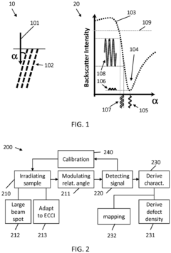
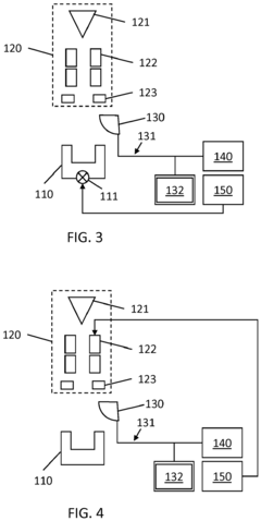
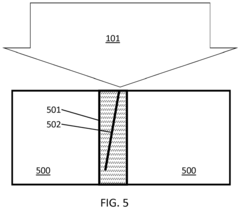
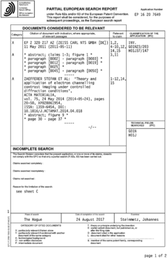
PatentActiveEP3343210A1
Innovation
- The method involves irradiating a sample with an electron beam modulated at a predetermined frequency to distinguish contributions from regions with different crystalline properties, allowing for enhanced sensitivity and reduced measurement time by decoupling signals from defect regions and the surrounding matrix using lock-in amplification techniques.
Sample Preparation Requirements
Sample preparation represents a critical determinant in the quality and reliability of both Atomic Force Microscopy (AFM) and Backscattered Electron Imaging (BEI) analyses. The two techniques impose distinctly different requirements that significantly impact their respective capabilities for clarity and depth measurement.
AFM sample preparation demands exceptionally clean, relatively flat surfaces with minimal topographical variations. Samples typically require thorough cleaning protocols to remove contaminants that could interfere with the cantilever tip movement. For biological specimens, fixation and dehydration procedures are necessary, though these may introduce artifacts. AFM samples can be examined in ambient conditions, vacuum, or liquid environments, offering flexibility for various specimen types. However, the physical interaction between the probe and sample surface necessitates careful mounting to prevent movement during scanning.
BEI preparation protocols focus primarily on conductivity and stability under electron bombardment. Samples generally require coating with conductive materials (carbon, gold, or platinum) to prevent charging artifacts when non-conductive. The preparation process for BEI is often more involved, requiring specialized equipment for coating and potentially polishing. Cross-sectional analysis demands precise cutting and polishing techniques to expose internal structures without introducing preparation artifacts.
The dimensional constraints differ significantly between the techniques. AFM samples must fit within the limited working area of the instrument (typically several millimeters) and exhibit height variations within the vertical range of the piezoelectric scanner (usually <10 μm). BEI accommodates larger specimens with dimensions up to several centimeters, depending on the chamber size of the scanning electron microscope.
Temperature sensitivity presents another critical consideration. AFM samples can experience thermal drift during measurement, potentially compromising resolution. BEI samples must withstand vacuum conditions and electron beam heating, which can damage heat-sensitive materials, particularly biological specimens.
These preparation requirements directly influence the techniques' capabilities. AFM's stringent surface flatness requirements limit its application for highly irregular samples but enable atomic-level resolution on well-prepared surfaces. BEI's conductivity requirements add preparation steps but allow for examination of a broader range of materials with minimal topographical limitations, offering superior depth analysis capabilities through backscattered electron penetration into the sample surface.
Cost-Benefit Analysis
When evaluating the implementation of Atomic Force Microscopy (AFM) versus Backscattered Electron Imaging (BSE), a comprehensive cost-benefit analysis reveals significant differences in initial investment, operational expenses, and long-term value proposition.
The initial acquisition costs present a stark contrast between these technologies. AFM systems typically range from $100,000 to $500,000 depending on capabilities and resolution requirements, while BSE equipment, often integrated into scanning electron microscopes (SEMs), represents an investment of $250,000 to $1,000,000. This higher initial outlay for BSE systems must be weighed against their multi-functionality within research environments.
Operational expenses further differentiate these technologies. AFM requires regular probe replacement ($200-500 per probe) with frequency depending on usage intensity and sample characteristics. Conversely, BSE systems demand higher energy consumption, specialized facility requirements including electromagnetic shielding, and vacuum systems maintenance, resulting in annual operational costs of $15,000-30,000 compared to AFM's $5,000-15,000.
Sample preparation costs vary significantly between methodologies. AFM samples generally require minimal preparation, often limited to cleaning procedures and occasional surface treatments. BSE imaging frequently necessitates conductive coating application, specialized mounting, and sometimes dehydration or fixation protocols, potentially adding $50-200 per sample versus $10-50 for AFM preparation.
Personnel training represents another critical cost factor. AFM operation typically requires 2-3 weeks of specialized training, while proficiency in BSE imaging demands 1-2 months of comprehensive instruction due to the complexity of electron microscopy systems and their associated parameters.
The return on investment calculation must incorporate application-specific benefits. AFM delivers superior value in applications requiring nanoscale topographical analysis, force measurements, and non-conductive sample imaging without modification. BSE provides greater benefits for compositional contrast imaging, subsurface feature detection, and high-throughput analysis of multiple samples.
Maintenance contracts and service agreements constitute a significant portion of lifetime costs, with AFM systems typically requiring annual service contracts of $5,000-15,000 compared to $20,000-40,000 for BSE systems. However, the multi-user capability of BSE systems often allows cost distribution across multiple research groups or departments, potentially improving the cost-per-use metric in institutional settings.
Unlock deeper insights with Patsnap Eureka Quick Research — get a full tech report to explore trends and direct your research. Try now!
Generate Your Research Report Instantly with AI Agent
Supercharge your innovation with Patsnap Eureka AI Agent Platform!