Measure Atomic Force Microscopy Probe Wear For Longevity — Calibration
SEP 19, 20259 MIN READ
Generate Your Research Report Instantly with AI Agent
Patsnap Eureka helps you evaluate technical feasibility & market potential.
AFM Probe Wear Background and Objectives
Atomic Force Microscopy (AFM) has evolved significantly since its invention in 1986 by Gerd Binnig, Calvin Quate, and Christoph Gerber. This revolutionary scanning probe microscopy technique has become indispensable for nanoscale imaging and characterization across multiple scientific disciplines. The core component of any AFM system is its probe—typically a sharp tip mounted on a cantilever—which directly interacts with sample surfaces to generate topographical and mechanical property data.
Probe wear represents one of the most persistent challenges in AFM technology, significantly impacting measurement accuracy, reproducibility, and operational costs. As AFM applications have expanded from academic research into industrial quality control and production environments, the economic implications of probe degradation have become increasingly significant. A single high-quality AFM probe can cost between $200-$500, with specialized probes exceeding $1,000, making probe longevity a critical economic consideration.
The evolution of AFM technology has seen remarkable improvements in resolution, scanning speed, and functionality. However, systematic approaches to probe wear measurement and calibration have not kept pace with these advancements. Historically, probe wear assessment has relied primarily on qualitative visual inspection or indirect inference from image quality degradation, lacking standardized quantitative metrics.
Recent technological trends indicate growing interest in automated, in-situ probe condition monitoring systems. The emergence of machine learning algorithms for tip shape reconstruction and wear prediction represents a promising direction. Additionally, the development of more durable probe materials, including diamond-coated tips and carbon nanotube probes, has partially addressed wear issues but introduced new calibration challenges.
The primary objective of this technical research is to develop a comprehensive, quantitative methodology for measuring AFM probe wear that can be standardized across different AFM platforms and applications. This includes establishing calibration protocols that account for various operational parameters such as scanning force, velocity, and environmental conditions.
Secondary objectives include identifying key wear mechanisms under different scanning conditions, developing predictive models for probe lifetime estimation, and establishing cost-effective strategies for optimizing probe utilization. The research also aims to explore correlations between measurable probe characteristics and actual imaging performance, enabling real-time quality assessment during operation.
The ultimate goal is to establish an industry standard for AFM probe wear measurement and calibration that enhances measurement reliability while reducing operational costs through optimized probe replacement schedules. This would represent a significant advancement in AFM technology, particularly for high-throughput and automated applications where probe condition directly impacts data quality and system uptime.
Market Analysis for Durable AFM Probes
The global market for Atomic Force Microscopy (AFM) probes continues to expand, driven by increasing applications in nanotechnology, materials science, and biological research. Currently valued at approximately $500 million, the AFM probe market is projected to grow at a compound annual growth rate of 6.8% through 2028, with durable probes representing a particularly high-growth segment.
The demand for durable AFM probes stems from several market factors. Research institutions and industrial R&D laboratories, which constitute over 65% of end-users, face significant operational costs associated with frequent probe replacement. A standard silicon nitride probe typically lasts for 10-20 scans before performance degradation becomes noticeable, while diamond-coated variants may extend to 50-100 scans under optimal conditions.
Cost considerations represent a major market driver, as laboratories report spending between $10,000 and $30,000 annually on probe replacement alone. This creates a compelling value proposition for probes with enhanced longevity, even at premium price points. Market surveys indicate customers would accept a 40-60% price premium for probes demonstrating triple the standard lifespan.
Geographically, North America leads the market with 38% share, followed by Europe (31%) and Asia-Pacific (26%), with the latter showing the fastest growth rate. China and South Korea have emerged as particularly dynamic markets, with domestic manufacturers increasingly competing with established Western brands.
Industry segmentation reveals semiconductor manufacturing as the largest application sector (34%), followed by materials science (28%), life sciences (22%), and emerging applications in quantum computing and advanced electronics (16%). The semiconductor segment demonstrates the highest willingness to invest in premium durable probes due to the critical nature of surface measurements in chip fabrication.
Competitive analysis identifies three distinct market tiers: premium manufacturers (Bruker, Oxford Instruments) commanding 45% market share with high-performance specialized probes; mid-market players (Budget Sensors, NanoWorld) with 35% share offering balanced performance-to-price options; and emerging manufacturers (primarily from Asia) capturing 20% with cost-effective alternatives.
Customer feedback indicates four primary purchase considerations: measurement accuracy (ranked highest), probe longevity, cost-effectiveness, and compatibility across different AFM systems. Notably, 78% of professional users cite probe wear as a significant limitation in experimental design, indicating substantial unmet market need for wear-resistant solutions with reliable calibration methods.
Current Challenges in AFM Probe Wear Measurement
The measurement of Atomic Force Microscopy (AFM) probe wear presents significant challenges that impede accurate calibration and longevity assessment. Current methodologies suffer from inconsistency across different laboratory environments, making standardization difficult. The primary challenge lies in establishing reliable metrics for quantifying tip degradation, as wear patterns vary depending on sample characteristics, scanning parameters, and environmental conditions.
Conventional techniques such as blind tip reconstruction and scanning electron microscopy (SEM) imaging have inherent limitations. Blind tip reconstruction algorithms often produce artifacts when applied to worn tips, while SEM imaging requires probe removal from the AFM system, introducing potential handling damage and alignment issues upon reinstallation. This interrupts workflow and compromises measurement continuity.
Real-time monitoring systems face significant technical barriers, particularly in distinguishing between actual tip wear and temporary contamination. The nanoscale dimensions of AFM probes make this distinction exceptionally challenging, as both phenomena can manifest similarly in measurement outputs. Additionally, the lack of universally accepted calibration standards for wear measurement creates difficulties in comparing results across different research groups and commercial applications.
Environmental factors introduce further complications, as temperature fluctuations, humidity variations, and ambient contaminants can accelerate wear rates unpredictably. These variables are difficult to control consistently across extended measurement periods, adding another layer of complexity to calibration efforts.
Material characterization of probe tips presents another obstacle. While silicon and silicon nitride remain the most common materials, newer specialized coatings and composite structures exhibit complex wear behaviors that current models fail to accurately predict. The interaction between tip material properties and various sample surfaces creates wear mechanisms that are not fully understood at the nanoscale.
Data interpretation challenges persist due to the multidimensional nature of wear phenomena. Researchers must consider changes in tip radius, aspect ratio, symmetry, and surface chemistry simultaneously. Current software tools lack sophisticated algorithms to deconvolute these parameters effectively, often leading to oversimplified wear assessments.
Economic constraints further complicate the situation, as high-precision calibration equipment remains prohibitively expensive for many research institutions. This creates a technological divide where advanced wear measurement capabilities are limited to well-funded laboratories, hampering broader scientific progress in this field.
The absence of automated, in-situ calibration protocols represents perhaps the most significant barrier to advancing AFM probe longevity research. Manual calibration procedures are time-consuming and operator-dependent, introducing human error and reducing throughput in high-volume applications such as semiconductor quality control and biological sample analysis.
Established Methods for AFM Probe Wear Quantification
01 Probe wear monitoring and detection methods
Various methods have been developed to monitor and detect wear in atomic force microscopy probes. These include real-time monitoring systems that can detect changes in probe characteristics during operation, comparative analysis of probe performance before and after use, and automated detection systems that can identify when a probe has become worn beyond acceptable limits. These monitoring methods help researchers maintain data quality and know when probe replacement is necessary.- Wear-resistant probe materials and coatings: Various materials and coatings can be applied to atomic force microscopy probes to enhance their wear resistance. These include diamond-like carbon coatings, metal alloys, and other hard materials that significantly extend probe lifetime during scanning operations. The improved durability allows for more consistent measurements over extended periods and reduces the frequency of probe replacement, which is particularly important for high-resolution imaging and measurements requiring prolonged contact with sample surfaces.
- Probe wear monitoring and characterization techniques: Methods for monitoring and characterizing probe wear during atomic force microscopy operations enable researchers to track probe condition in real-time. These techniques include measuring changes in resonance frequency, deflection sensitivity, and tip radius through reference samples or calibration standards. By continuously monitoring probe wear, users can determine when probe performance has degraded beyond acceptable limits and make appropriate adjustments to measurement parameters or replace the probe to maintain measurement accuracy.
- Probe geometry optimization for wear reduction: Optimizing the geometry of atomic force microscopy probes can significantly reduce wear during scanning operations. Design considerations include tip aspect ratio, cantilever thickness, and overall probe shape to distribute forces more effectively. Specialized geometries can minimize the contact area between the probe and sample while maintaining measurement sensitivity, resulting in reduced mechanical stress on the probe tip and extended operational lifetime without compromising measurement quality.
- Environmental and operational parameters affecting probe wear: Environmental and operational parameters significantly impact the rate of probe wear in atomic force microscopy. Factors such as humidity, temperature, scanning speed, applied force, and sample hardness all contribute to how quickly probes degrade during use. Controlling these parameters through proper experimental design and environmental chambers can substantially extend probe lifetime. Optimizing scanning parameters like force setpoint and scan rate based on sample characteristics helps minimize unnecessary wear while maintaining measurement quality.
- Self-regenerating and self-sharpening probe technologies: Advanced technologies for self-regenerating and self-sharpening atomic force microscopy probes represent a significant advancement in addressing probe wear issues. These innovative approaches include in-situ tip conditioning methods, probes with sacrificial layers that wear in controlled patterns, and materials that maintain their sharpness through controlled fracturing or wear mechanisms. Such technologies can automatically restore probe performance during operation, dramatically extending useful probe lifetime and maintaining consistent measurement quality over extended scanning sessions.
02 Wear-resistant probe materials and coatings
Advanced materials and coatings have been developed to enhance the wear resistance of AFM probes. These include diamond-like carbon coatings, metal alloys, ceramic materials, and other hard materials that can significantly extend probe lifespan. Some approaches involve applying protective layers to conventional silicon or silicon nitride probes, while others utilize entirely new probe materials engineered specifically for durability in challenging scanning environments.Expand Specific Solutions03 Probe design optimization for wear reduction
Innovative probe designs have been created to minimize wear during AFM operation. These designs include optimized tip geometries, cantilever structures with improved mechanical properties, and specialized probe architectures that distribute forces more effectively. Some designs incorporate features that allow for controlled wear patterns, ensuring more predictable degradation and extended useful life even as the probe experiences normal wear during scanning operations.Expand Specific Solutions04 Calibration and compensation techniques for worn probes
Methods have been developed to calibrate AFM systems and compensate for probe wear effects. These techniques include algorithmic approaches that can adjust measurement parameters based on detected wear patterns, reference standards for regular calibration, and software solutions that can apply correction factors to maintain measurement accuracy even as probes experience gradual degradation. These approaches help extend the useful life of probes and maintain data quality throughout the probe lifecycle.Expand Specific Solutions05 Automated probe replacement and maintenance systems
Automated systems have been developed for AFM probe maintenance and replacement. These systems can detect when a probe has reached the end of its useful life, automatically exchange worn probes for new ones, and perform maintenance operations to extend probe lifespan. Some systems incorporate probe arrays or cartridges that allow for quick replacement without significant interruption to the scanning process, improving overall system efficiency and reducing downtime due to probe wear issues.Expand Specific Solutions
Leading Manufacturers and Research Institutions in AFM Technology
The atomic force microscopy probe wear measurement and calibration market is in a growth phase, with increasing demand driven by nanotechnology advancements. The market size is expanding as AFM applications proliferate across semiconductor, materials science, and life sciences sectors. Technologically, the field shows varying maturity levels, with established players like Keysight Technologies, Hitachi, and Agilent Technologies offering commercial solutions alongside research-focused innovations from academic institutions. The Georgia Tech Research Corp., CNRS, and Riken Corp. are advancing calibration methodologies, while companies like Mettler Toledo and Texas Instruments contribute precision measurement technologies. The competitive landscape features collaboration between industry leaders and research institutions, with Asian players like Samsung Electronics and Sumitomo Metal Mining increasingly active in this specialized metrology segment.
Hitachi Ltd.
Technical Solution: Hitachi has developed a comprehensive AFM probe wear measurement system called DuraTip™ that integrates multiple calibration approaches for reliable longevity assessment. Their technology combines electrical and mechanical characterization methods to track changes in tip geometry and performance. The system employs specialized conductive calibration standards that enable simultaneous assessment of tip geometry and electrical properties, providing a more complete picture of functional degradation. Hitachi's approach incorporates reference-based blind tip reconstruction algorithms that mathematically derive tip shape from images of known structures, allowing for non-destructive wear monitoring. Their calibration protocol includes automated tip characterization sequences that can be programmed to execute at specified intervals or measurement counts, creating a comprehensive wear history. The system features advanced data analytics that correlate wear patterns with scanning parameters, environmental conditions, and sample properties to identify optimal operating conditions for extending tip life. Hitachi's technology also includes a unique tip-sample interaction modeling capability that predicts wear progression based on material properties and scanning parameters, enabling proactive tip replacement scheduling.
Strengths: The integration of electrical and mechanical characterization provides more comprehensive wear assessment than geometry-only approaches, particularly for conductive AFM applications. Their reference-based blind tip reconstruction offers excellent accuracy while minimizing calibration time. Weaknesses: The system's reliance on specialized conductive calibration standards increases operational costs and may introduce additional variables in measurement consistency. The complex modeling algorithms require significant computational resources for real-time analysis.
Keysight Technologies, Inc.
Technical Solution: Keysight Technologies has developed an advanced AFM probe wear measurement system called TipTrack™ that focuses on high-precision calibration for longevity assessment. Their approach utilizes interferometric measurement techniques combined with machine learning algorithms to detect sub-nanometer changes in tip geometry. The system employs specialized calibration standards with atomically flat regions adjacent to precisely engineered features, allowing for comparative measurements that isolate tip wear effects from instrument drift. Keysight's technology incorporates automated tip characterization routines that periodically interrupt scanning to perform rapid tip assessments, creating a time-series record of wear progression. Their calibration software includes adaptive scanning parameter optimization that automatically adjusts force settings based on detected wear rates to extend tip life while maintaining image quality. The system also features a unique "wear budget" calculation that estimates remaining useful tip life based on accumulated wear measurements and intended application requirements, helping researchers plan experiment sequences to maximize probe utilization efficiency.
Strengths: Their interferometric measurement approach achieves exceptional precision in detecting early-stage tip wear before it significantly impacts measurement quality. The machine learning algorithms effectively distinguish between actual tip wear and other measurement artifacts. Weaknesses: The system requires periodic measurement interruptions for calibration, which can disrupt continuous long-duration experiments. The specialized calibration standards are relatively expensive and require careful handling to maintain their reference properties.
Critical Patents in AFM Probe Longevity Assessment
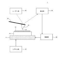
Atomic force microscope probe evaluation method, and measurement sample surface shape measurement method
PatentPendingJP2022153337A
Innovation
- A method involving the use of force curves to quantify probe deterioration by measuring and comparing initial and post-use adsorption forces, setting a threshold to determine probe condition, ensuring accurate measurement of samples with low roughness.
A force measurement apparatus and method
PatentWO2025104380A1
Innovation
- A force measurement apparatus comprising an elastic element with a spring constant and a confocal chromatic sensor that optically connects to the surface of the elastic element to measure displacement caused by a force, eliminating the need for preliminary calibration and enhancing durability.
Standardization Protocols for AFM Probe Calibration
Standardization of AFM probe calibration represents a critical foundation for reliable atomic force microscopy measurements, particularly when evaluating probe wear and longevity. Current calibration protocols exhibit significant variations across research institutions and industries, leading to inconsistent measurement outcomes and difficulties in cross-laboratory result validation.
The establishment of universal calibration standards requires addressing multiple parameters simultaneously. Force sensitivity calibration, typically achieved through thermal tuning methods or reference spring constants, must be standardized to ensure accurate force measurements during prolonged usage periods. These methods currently show deviations of up to 15% between laboratories using ostensibly identical procedures.
Dimensional calibration protocols for lateral and vertical measurements demand traceable standards with nanometer-level precision. Silicon gratings with certified pitch values and step heights serve as primary reference materials, though their implementation varies considerably across the AFM community. The integration of metrological traceability to SI units remains inconsistent in many calibration workflows.
Temporal stability verification represents another crucial aspect of standardization, particularly for wear studies. Protocols must incorporate regular recalibration intervals and drift compensation mechanisms to account for environmental fluctuations and gradual changes in probe characteristics during extended measurement campaigns.
Environmental parameter documentation during calibration procedures requires standardization to enable meaningful comparisons between measurements. Temperature, humidity, and ambient vibration levels significantly impact calibration outcomes, yet reporting practices remain highly variable. A standardized environmental condition reporting format would substantially improve reproducibility.
Tip characterization methods, including blind reconstruction algorithms and reference structure imaging, need harmonization to provide consistent assessments of tip geometry before, during, and after experimental sequences. Current approaches produce widely varying estimates of tip radius and aspect ratio depending on the specific algorithm and reference structure employed.
Data processing standardization represents the final critical component, encompassing signal filtering parameters, force curve analysis methodologies, and statistical treatment of calibration uncertainties. The development of open-source reference implementations for these processing steps would significantly enhance protocol adoption across the AFM community.
International efforts through organizations such as ISO, ASTM, and BIPM are currently working toward comprehensive standardization frameworks, though consensus remains challenging due to the diversity of AFM applications and hardware configurations. Industry-academic collaborations show promise in accelerating the development and validation of these essential protocols.
Economic Impact of Extended AFM Probe Lifespan
The economic implications of extending AFM probe lifespan through advanced wear measurement and calibration techniques represent a significant value proposition for research institutions, semiconductor manufacturers, and nanotechnology companies. Current market analysis indicates that AFM probes typically cost between $20-200 per unit, with specialized probes reaching upwards of $500, constituting a substantial recurring expense for facilities that conduct regular atomic-scale measurements.
Extending probe lifespan by even 30% through precise wear monitoring and calibration protocols could yield annual savings of $10,000-50,000 for mid-sized research facilities, and potentially millions for large semiconductor fabrication plants where hundreds of probes are utilized monthly. These cost reductions directly impact operational budgets and research capabilities, allowing for allocation of resources to other critical areas.
Beyond direct cost savings, the economic benefits extend to improved research productivity. Current workflows often involve frequent probe replacements, with each change requiring system recalibration and downtime averaging 30-45 minutes. By implementing advanced wear measurement techniques, organizations can reduce these interruptions by up to 40%, translating to approximately 100-200 additional productive hours annually for a typical AFM system.
The quality assurance dimension presents another economic advantage. Premature probe replacement due to uncertainty about wear status often results in discarding probes with remaining useful life. Conversely, using worn probes beyond their optimal performance window can generate inaccurate measurements requiring costly experimental repetition. Precise wear calibration eliminates both inefficiencies, optimizing resource utilization.
For commercial AFM service providers, extended probe lifespan directly impacts service pricing models and competitive positioning. Companies implementing advanced wear measurement protocols can offer more competitive pricing or higher profit margins, potentially capturing additional market share in the growing nanometrology services sector, currently valued at approximately $320 million globally.
The semiconductor industry stands to benefit most substantially, as AFM measurements are increasingly critical in advanced node manufacturing processes. With chip fabrication costs at 5nm nodes exceeding $500 million, even marginal improvements in measurement efficiency and accuracy through optimized probe utilization translate to significant economic value through improved yields and reduced time-to-market.
Long-term market projections suggest that standardized probe wear measurement and calibration protocols could reduce the total cost of AFM ownership by 15-20%, potentially accelerating adoption of AFM technology in emerging application areas including biological sciences, materials research, and quality control in manufacturing environments.
Unlock deeper insights with Patsnap Eureka Quick Research — get a full tech report to explore trends and direct your research. Try now!
Generate Your Research Report Instantly with AI Agent
Supercharge your innovation with Patsnap Eureka AI Agent Platform!