

How To Leverage Atomic Force Microscopy In Nanotechnology — Techniques
SEP 19, 202510 MIN READ
Generate Your Research Report Instantly with AI Agent
Patsnap Eureka helps you evaluate technical feasibility & market potential.
AFM in Nanotechnology: Background and Objectives
Atomic Force Microscopy (AFM) has emerged as a revolutionary tool in the field of nanotechnology since its invention in 1986 by Gerd Binnig, Calvin Quate, and Christoph Gerber. This scanning probe microscopy technique has evolved from a simple imaging tool to a sophisticated platform capable of manipulating matter at the atomic scale. The technological trajectory of AFM has been marked by continuous improvements in resolution, functionality, and application scope, making it an indispensable instrument in nanoscience research and development.
The evolution of AFM technology has been characterized by several significant milestones. Initially limited to topographical imaging in ambient conditions, modern AFM systems now operate in various environments including vacuum, liquid, and controlled atmospheres. The development of specialized probes, feedback mechanisms, and detection systems has dramatically enhanced the capabilities of AFM, enabling not only imaging but also nanomechanical characterization, electrical measurements, and nanomanipulation.
Current technological trends in AFM include the integration with complementary techniques such as Raman spectroscopy, infrared spectroscopy, and electron microscopy, creating powerful hybrid systems that provide multidimensional data about nanoscale phenomena. Additionally, there is a growing emphasis on high-speed AFM, which allows for real-time observation of dynamic processes at the nanoscale, opening new avenues for understanding biological systems and material behaviors.
The primary objective of leveraging AFM in nanotechnology is to bridge the gap between fundamental nanoscale phenomena and practical applications. This involves utilizing AFM's unique capabilities to characterize, manipulate, and fabricate structures at the nanoscale with unprecedented precision and control. Specific technical goals include enhancing spatial resolution beyond current limits, improving measurement speed without sacrificing accuracy, and developing more sophisticated data analysis algorithms to extract meaningful information from complex AFM datasets.
Another critical objective is the standardization of AFM techniques and protocols to ensure reproducibility and comparability of results across different laboratories and instruments. This is particularly important as AFM transitions from a primarily research tool to a key enabling technology in industrial applications such as semiconductor manufacturing, pharmaceutical development, and advanced materials engineering.
Looking forward, the integration of artificial intelligence and machine learning with AFM represents a promising frontier. These technologies could potentially automate complex measurement procedures, identify patterns in large datasets, and even predict material behaviors based on AFM measurements, thereby accelerating the pace of discovery and innovation in nanotechnology.
Market Applications and Demand Analysis for AFM Technologies
The global market for Atomic Force Microscopy (AFM) technologies has experienced significant growth, driven primarily by expanding applications in nanotechnology research and development. The current market valuation stands at approximately 500 million USD with a compound annual growth rate of 6.8% projected through 2028, reflecting the increasing adoption of AFM across multiple industries.
Material science represents the largest application segment, accounting for nearly 30% of the total AFM market. The demand stems from the need to characterize surface properties, mechanical behaviors, and atomic-scale structures of novel materials. Particularly, the development of advanced composites, smart materials, and nanomaterials has intensified the requirement for high-precision AFM technologies capable of providing three-dimensional topographical imaging at the nanoscale.
The semiconductor and electronics industry constitutes another substantial market segment, where AFM technologies are essential for quality control in chip manufacturing, failure analysis, and research into next-generation electronic components. With the continuous miniaturization of electronic devices and the emergence of quantum computing, the demand for AFM systems with enhanced resolution and specialized probes has surged significantly.
Life sciences and pharmaceutical research represent the fastest-growing application segment, with an estimated growth rate of 8.5% annually. AFM's ability to operate in liquid environments makes it invaluable for studying biological samples under physiological conditions. The technology enables researchers to visualize and manipulate biomolecules, investigate cell mechanics, and analyze drug-target interactions at the molecular level, driving innovation in drug discovery and personalized medicine.
Regionally, North America dominates the AFM market with approximately 35% share, followed closely by Europe and Asia-Pacific. However, the Asia-Pacific region is experiencing the most rapid growth, primarily due to increasing investments in nanotechnology research infrastructure in China, Japan, South Korea, and Singapore.
End-user analysis reveals that academic and research institutions remain the primary consumers of AFM technologies, accounting for roughly 45% of the market. However, industrial applications are growing at a faster rate as manufacturing companies increasingly incorporate AFM into their quality control and R&D processes.
Market trends indicate a growing demand for automated AFM systems with improved user interfaces, reduced complexity, and higher throughput capabilities. Additionally, there is increasing interest in specialized AFM techniques such as conductive AFM, magnetic force microscopy, and kelvin probe force microscopy, which provide additional material characterization capabilities beyond standard topographical imaging.
Current AFM Capabilities and Technical Challenges
Atomic Force Microscopy (AFM) has evolved significantly since its invention in 1986, becoming a cornerstone technology in nanoscale research and development. Current AFM systems offer remarkable capabilities, including sub-nanometer resolution in three dimensions, operation in various environments (vacuum, air, liquid), and compatibility with biological samples. Modern instruments can achieve scan rates of several frames per second for dynamic processes observation and force sensitivity down to piconewtons, enabling molecular interaction studies.
Despite these advancements, AFM faces several technical challenges that limit its broader application. Scan speed remains a significant constraint, with high-resolution imaging typically requiring minutes to hours per frame, making real-time monitoring of rapid nanoscale processes difficult. This limitation stems from mechanical resonance issues in the cantilever system and feedback loop response times.
Tip degradation presents another persistent challenge. The probe tip, crucial for resolution quality, experiences wear during scanning, particularly on hard or rough surfaces. This degradation leads to inconsistent imaging results and necessitates frequent tip replacement, increasing operational costs and reducing experimental continuity. While super-sharp tips and tip-preservation techniques exist, they often involve trade-offs in durability or sample compatibility.
Quantitative data interpretation remains complex due to tip-sample interaction artifacts. Forces between the tip and sample can cause deformation, especially in soft materials, leading to measurement inaccuracies. Additionally, environmental factors such as temperature fluctuations and acoustic vibrations can introduce noise, requiring sophisticated isolation systems that add to instrument complexity and cost.
For biological applications, maintaining sample viability during imaging presents unique challenges. The forces applied during scanning, though minimal, can still disrupt delicate biological structures. Furthermore, achieving molecular-level chemical identification directly through AFM remains limited, often requiring integration with complementary techniques like Raman spectroscopy or infrared spectroscopy.
Automation and user accessibility represent ongoing development areas. Despite advances in software interfaces, AFM operation still requires significant expertise for optimal results. The learning curve remains steep for new users, and parameter optimization often relies heavily on operator experience rather than standardized protocols. This expertise barrier limits AFM adoption in routine industrial applications and educational settings.
Addressing these challenges requires interdisciplinary approaches combining advances in materials science, electronics, software algorithms, and mechanical design. Recent developments in high-speed AFM, machine learning for image processing, and multimodal systems that combine AFM with complementary techniques show promising directions for overcoming current limitations.
Contemporary AFM Methodologies and Implementation Strategies
01 Basic AFM Imaging Techniques
Atomic Force Microscopy (AFM) employs various imaging techniques to analyze surface topography at the nanoscale. These techniques involve scanning a sharp tip across a sample surface while measuring the forces between the tip and sample. Different modes such as contact mode, tapping mode, and non-contact mode allow for versatile surface characterization with high resolution. These fundamental techniques form the basis for more specialized AFM applications.- Advanced AFM Imaging Techniques: Various advanced imaging techniques in atomic force microscopy enable high-resolution visualization of surface structures at the nanoscale. These techniques include tapping mode, non-contact mode, and phase imaging that allow for detailed characterization of sample topography and properties while minimizing damage to delicate samples. These methods can be optimized for different sample types and environmental conditions to enhance image quality and data acquisition.
- AFM Probe Design and Modification: Specialized probe designs and modifications significantly enhance atomic force microscopy capabilities. These include functionalized tips with specific chemical groups, high-aspect-ratio probes for imaging deep trenches, and probes with integrated sensors. Advanced manufacturing techniques allow for precise control of tip geometry and surface properties, enabling measurements of various physical, chemical, and biological interactions at the nanoscale with improved sensitivity and specificity.
- Multimodal and Specialized AFM Applications: Multimodal atomic force microscopy combines traditional AFM with other analytical techniques to provide comprehensive sample characterization. These hybrid approaches include combining AFM with infrared spectroscopy, Raman spectroscopy, or electrical measurements. Specialized applications have been developed for biological samples, semiconductor analysis, and materials science, allowing researchers to simultaneously obtain topographical, mechanical, electrical, and chemical information from samples at nanometer resolution.
- AFM Force Measurement and Spectroscopy: Force measurement and spectroscopy techniques in atomic force microscopy enable quantitative analysis of nanomechanical properties and molecular interactions. These methods include force-distance curve analysis, nanoindentation, and single-molecule force spectroscopy. By precisely controlling the interaction between the AFM tip and sample, researchers can measure adhesion forces, elasticity, stiffness, and other mechanical properties at specific points on a sample surface with piconewton sensitivity.
- AFM Instrumentation and Control Systems: Advanced instrumentation and control systems have revolutionized atomic force microscopy performance and usability. These developments include high-precision piezoelectric scanners, improved feedback control algorithms, and noise reduction technologies. Automated systems for tip approach, engagement, and parameter optimization have made AFM more accessible while enhancing measurement reproducibility. Integration with computational methods allows for real-time data processing and analysis, significantly improving throughput and enabling new applications in research and industry.
02 Advanced AFM Probe Technologies
Innovations in AFM probe design have significantly enhanced measurement capabilities. Specialized probes with functionalized tips enable detection of specific molecular interactions, electrical properties, and mechanical characteristics. These advanced probes may incorporate novel materials, coatings, or integrated sensors that improve sensitivity, durability, and measurement precision. Such technological advancements expand the analytical capabilities of atomic force microscopy across various scientific disciplines.Expand Specific Solutions03 Multimodal and Specialized AFM Techniques
Beyond conventional imaging, AFM has evolved to incorporate multiple measurement modes simultaneously. These multimodal techniques combine topographical imaging with measurements of electrical, magnetic, thermal, or mechanical properties. Specialized techniques such as Kelvin probe force microscopy, piezoresponse force microscopy, and force spectroscopy provide comprehensive characterization of sample properties at the nanoscale. These advanced methods enable researchers to correlate various physical properties with surface features.Expand Specific Solutions04 AFM Data Processing and Analysis Methods
Sophisticated data processing algorithms and analysis methods are essential for extracting meaningful information from AFM measurements. These include noise reduction techniques, drift correction, statistical analysis tools, and image processing methods specifically designed for AFM data. Advanced software solutions enable automated feature recognition, quantitative analysis of surface properties, and three-dimensional visualization of results. These computational approaches enhance the accuracy and interpretability of atomic force microscopy data.Expand Specific Solutions05 Environmental and In-situ AFM Applications
AFM techniques have been adapted for operation under various environmental conditions and for in-situ measurements. These include liquid-phase AFM for biological samples, high-temperature or controlled-atmosphere chambers, and integration with complementary analytical techniques. Such environmental adaptations enable real-time observation of dynamic processes, including chemical reactions, biological interactions, and material transformations at the nanoscale. These specialized setups expand the application range of atomic force microscopy to more realistic experimental conditions.Expand Specific Solutions
Leading Manufacturers and Research Institutions in AFM
Atomic Force Microscopy (AFM) in nanotechnology is currently in a mature growth phase, with the global market expected to reach significant expansion due to increasing applications in materials science, biology, and semiconductor industries. The technology has evolved from basic imaging to advanced characterization techniques, with key players demonstrating varying levels of technical sophistication. Leading research institutions like Tsinghua University, CSIC, and University of California are advancing fundamental AFM methodologies, while commercial entities such as Bruker Nano, IBM, and LG Electronics are developing application-specific innovations. The competitive landscape shows a balanced distribution between academic research centers pushing theoretical boundaries and corporate players focusing on practical implementations, with Asian institutions particularly active in emerging AFM techniques for nanomaterial characterization.
Consejo Superior de Investigaciones Científicas
Technical Solution: The Consejo Superior de Investigaciones Científicas (CSIC) has developed innovative AFM techniques for nanotechnology applications through their specialized research institutes. Their approach combines dynamic AFM modes with advanced signal processing to achieve atomic resolution imaging in various environments, including liquid and vacuum conditions[1]. CSIC researchers have pioneered multifrequency AFM techniques that excite and detect multiple cantilever resonances simultaneously, extracting complementary information about sample properties beyond conventional topography[2]. They've also developed specialized probes with functionalized tips for chemical identification at the nanoscale. Their bimodal AFM technique enables simultaneous acquisition of mechanical and electrical properties by operating the cantilever at two resonance frequencies. Additionally, CSIC has created advanced force spectroscopy methods that can map nanomechanical properties with high spatial resolution while minimizing sample damage, particularly valuable for soft biological materials and polymer nanocomposites[3]. Their 3D-AFM technology allows for volumetric imaging by precisely controlling the tip trajectory in three dimensions.
Strengths: Cutting-edge research in multifrequency and bimodal AFM techniques; strong focus on fundamental physics of tip-sample interactions; excellent capabilities for liquid environment imaging. Weaknesses: More focused on research applications than commercial development; techniques often require custom modifications to commercial instruments; limited global distribution network compared to commercial entities.
Bruker Nano, Inc.
Technical Solution: Bruker Nano has developed advanced atomic force microscopy (AFM) systems specifically designed for nanotechnology applications. Their PeakForce Tapping technology enables high-resolution imaging while protecting delicate samples by precisely controlling tip-sample interaction forces[1]. This technique automatically optimizes imaging parameters and provides quantitative nanomechanical mapping of properties like modulus, adhesion, and deformation. Bruker's FastScan technology allows for imaging speeds up to 20 times faster than conventional AFMs while maintaining resolution[2]. Their BioScope Resolve platform integrates optical microscopy with AFM for correlative imaging in biological samples. Additionally, Bruker has pioneered PeakForce QNM (Quantitative Nanomechanical Mapping) which simultaneously acquires topographical data and mechanical properties at the nanoscale, enabling researchers to characterize complex materials with unprecedented detail and efficiency[3].
Strengths: Industry-leading resolution capabilities with proprietary PeakForce technology; comprehensive suite of specialized modes for different applications; excellent integration with other analytical techniques. Weaknesses: High cost of equipment and maintenance; steep learning curve for new users; some specialized modes require additional expensive accessories.
Critical Patents and Innovations in AFM Technology
Methods and apparatus for atomic force microscopy
PatentInactiveUS20030160170A1
Innovation
- The cantilever probe is arranged with its axis perpendicular to the sample presentation plane, featuring a rearwardly-directed reflection surface for beam detection, allowing lateral oscillation and enhanced access to sample surfaces, including steep features, and enabling true tip-sample distance control through axial adjustment.
Atomic force microscopy using correlated probe oscillation and probe-sample bias voltage
PatentInactiveUS20150276795A1
Innovation
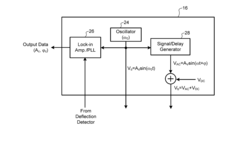
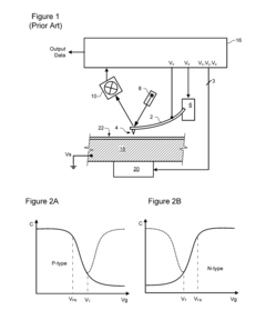
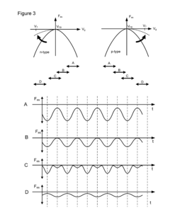
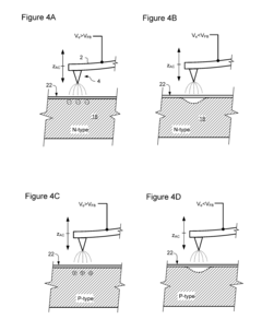
- The method involves generating a periodic motion of a probe tip with a correlated oscillatory bias signal, analyzing the response to infer semiconductor surface properties without requiring additional capacitance sensors, leveraging asymmetric electrostatic force-bias curves to differentiate between p-type and n-type semiconductors based on cantilever dynamics.
Integration of AFM with Complementary Nanoscale Techniques
The integration of Atomic Force Microscopy (AFM) with complementary nanoscale techniques represents a significant advancement in nanotechnology research capabilities. This synergistic approach combines the high-resolution imaging and force measurement capabilities of AFM with other specialized techniques to provide comprehensive characterization of nanomaterials and nanostructures.
One of the most valuable integrations is AFM with optical microscopy techniques, particularly confocal microscopy and Raman spectroscopy. These combinations enable simultaneous topographical imaging and chemical composition analysis at the nanoscale. AFM-Raman systems can correlate mechanical properties with molecular structure, offering unprecedented insights into material characteristics without destructive sample preparation.
AFM-SEM (Scanning Electron Microscopy) and AFM-TEM (Transmission Electron Microscopy) hybrid systems have emerged as powerful tools for correlative microscopy. These integrations allow researchers to obtain complementary information about sample morphology, structure, and composition across different length scales. The AFM component provides three-dimensional surface topography and mechanical properties, while electron microscopy delivers high-resolution imaging and elemental analysis capabilities.
Electrical measurement techniques have also been successfully integrated with AFM, creating specialized variants such as Conductive AFM (C-AFM), Electrostatic Force Microscopy (EFM), and Kelvin Probe Force Microscopy (KPFM). These techniques enable simultaneous mapping of topography and electrical properties including conductivity, surface potential, and work function, which are critical parameters for semiconductor and electronic materials research.
Thermal analysis integration has led to the development of Scanning Thermal Microscopy (SThM), where specialized thermal probes can map temperature distributions and thermal conductivity variations at nanoscale resolution. This capability is particularly valuable for studying heat transfer in microelectronic devices and thermoelectric materials.
Near-field scanning optical microscopy (NSOM/SNOM) integration with AFM overcomes the diffraction limit of conventional optical microscopy, enabling optical characterization with nanoscale spatial resolution. This combination is particularly useful for studying plasmonic structures, photonic crystals, and optoelectronic devices.
Recent advances in high-speed AFM have facilitated integration with time-resolved spectroscopic techniques, allowing researchers to study dynamic processes at the nanoscale. These developments have opened new avenues for investigating biological processes, chemical reactions, and phase transitions with unprecedented temporal and spatial resolution.
The integration challenges primarily involve alignment precision, probe design optimization, and data correlation across different measurement modalities. However, continued technological advancements are progressively addressing these limitations, expanding the application scope of integrated AFM systems across materials science, biology, and semiconductor research.
Standardization and Calibration Protocols for AFM Measurements
Standardization and calibration protocols are fundamental to ensuring the reliability, reproducibility, and comparability of Atomic Force Microscopy (AFM) measurements in nanotechnology applications. The establishment of robust protocols addresses the inherent variability in AFM instrumentation and measurement conditions that can significantly impact data quality and interpretation.
International standards organizations, including ISO and ASTM, have developed specific guidelines for AFM calibration procedures. These standards cover critical aspects such as probe characterization, scanner calibration, and force calibration. For instance, ISO 11775 provides detailed procedures for calibrating the lateral and vertical displacement of AFM scanners, ensuring dimensional accuracy across different instruments.
Probe calibration represents a critical component of AFM standardization protocols. This includes characterization of cantilever spring constants, tip geometry, and resonance frequencies. The thermal noise method has emerged as a widely accepted approach for determining cantilever spring constants, offering non-destructive calibration with minimal sample interaction. For tip geometry characterization, reference standards with well-defined structures, such as silicon gratings with precise pitch dimensions, enable consistent tip shape determination.
Scanner calibration protocols address both the linearity and orthogonality of the piezoelectric scanning elements. Calibration artifacts with certified dimensions, including calibration gratings and step height standards, provide reference measurements for adjusting scanner response. Advanced protocols incorporate compensation for piezoelectric hysteresis and creep effects, which can introduce significant measurement errors if left uncorrected.
Force calibration standardization ensures consistent force measurements across different AFM systems. This involves calibrating the photodetector sensitivity and correlating cantilever deflection with applied force. Reference materials with known mechanical properties, such as elasticity standards, facilitate validation of force measurement accuracy and enable cross-laboratory comparability.
Environmental parameter control constitutes another critical aspect of AFM standardization. Protocols specify acceptable ranges for temperature, humidity, and vibration levels, along with procedures for monitoring and documenting these conditions during measurements. Some advanced protocols incorporate real-time environmental compensation algorithms to minimize drift and thermal expansion effects.
Data processing and analysis standardization complements hardware calibration protocols. These guidelines establish consistent approaches for image flattening, filtering, and feature measurement. Standardized reporting formats ensure that calibration parameters and measurement conditions are properly documented, facilitating data sharing and meta-analysis across research groups.
Implementation of these standardization and calibration protocols significantly enhances measurement reliability in nanotechnology applications, enabling quantitative analysis with known uncertainty levels and facilitating meaningful comparisons between measurements performed on different instruments or by different operators.
Unlock deeper insights with Patsnap Eureka Quick Research — get a full tech report to explore trends and direct your research. Try now!
Generate Your Research Report Instantly with AI Agent
Supercharge your innovation with Patsnap Eureka AI Agent Platform!