

Atomic Force Microscopy Vs Electron Microscopy: Pros, Cons, Applications
SEP 19, 20259 MIN READ
Generate Your Research Report Instantly with AI Agent
Patsnap Eureka helps you evaluate technical feasibility & market potential.
Microscopy Evolution and Research Objectives
Microscopy has undergone a remarkable evolution since the invention of the first optical microscope in the late 16th century. This journey has been characterized by continuous technological advancements, pushing the boundaries of what scientists can observe at increasingly smaller scales. The transition from optical to electron microscopy in the early 20th century represented a quantum leap in resolution capabilities, enabling visualization at the nanometer scale. More recently, the development of scanning probe techniques, particularly Atomic Force Microscopy (AFM) in the 1980s, has further expanded our ability to examine surfaces at the atomic level.
The parallel development of Electron Microscopy (EM) and Atomic Force Microscopy represents divergent yet complementary approaches to nanoscale imaging. Electron microscopy, including Transmission Electron Microscopy (TEM) and Scanning Electron Microscopy (SEM), utilizes electron beams to achieve high-resolution imaging. In contrast, AFM employs a physical probe to map surface topography through mechanical interactions, offering unique capabilities for three-dimensional surface characterization.
Current research objectives in microscopy technology focus on overcoming the inherent limitations of both AFM and EM techniques. For AFM, researchers aim to improve scanning speeds, enhance force sensitivity, and develop more sophisticated probe technologies to expand its application range. In the EM field, efforts concentrate on reducing beam damage to sensitive samples, improving resolution under diverse environmental conditions, and developing in-situ capabilities for dynamic observations.
A significant trend in contemporary microscopy research is the integration of multiple imaging modalities. Correlative microscopy approaches that combine the strengths of AFM and EM are gaining prominence, allowing researchers to obtain complementary data sets from the same sample region. This integration aims to provide more comprehensive characterization by leveraging the surface sensitivity of AFM with the high-resolution capabilities of EM.
Another key objective is the advancement of environmental and in-situ microscopy capabilities. Both AFM and EM technologies are evolving to enable observations under more realistic conditions, moving beyond traditional high-vacuum or ambient air environments to include liquid media, controlled atmospheres, and variable temperatures. These developments are particularly crucial for biological and materials science applications where sample behavior under native conditions is of paramount importance.
The ultimate goal of current microscopy research is to achieve atomic-scale resolution across diverse sample types while maintaining the ability to observe dynamic processes in real-time. This ambitious objective drives innovation in instrumentation, detection systems, and data processing algorithms, pushing toward a future where the nanoscale world becomes increasingly accessible to scientific investigation.
Market Applications and Industry Demand
The microscopy market has witnessed significant growth in recent years, driven by increasing applications across various industries. Atomic Force Microscopy (AFM) and Electron Microscopy (EM) represent two distinct yet complementary technologies that serve different market segments with unique value propositions.
The global microscopy market was valued at approximately $7.8 billion in 2022, with projections indicating growth to reach $12.7 billion by 2028. Within this market, electron microscopy holds the largest share at around 40%, while AFM represents about 15% with faster growth rates due to emerging applications in nanotechnology and materials science.
Healthcare and life sciences constitute the largest application segment for both technologies, accounting for nearly 35% of the total market. In this sector, electron microscopy dominates clinical diagnostics and pathology, while AFM finds increasing applications in drug discovery and biomolecular research. The pharmaceutical industry particularly values AFM for its ability to analyze drug-target interactions at the molecular level without damaging sensitive biological samples.
Semiconductor and electronics manufacturing represents the second-largest market segment, contributing approximately 28% to the overall microscopy market. Here, electron microscopy remains essential for quality control and failure analysis, while AFM has become indispensable for surface characterization and nanolithography processes in advanced chip manufacturing.
Materials science research accounts for about 20% of the market, with both technologies seeing strong demand. AFM has gained significant traction in this sector due to its superior capabilities in measuring mechanical properties and surface topography of novel materials, including polymers, composites, and 2D materials.
Regional analysis reveals North America as the largest market (32%), followed closely by Asia-Pacific (30%), which demonstrates the fastest growth rate due to expanding semiconductor industries in countries like Taiwan, South Korea, and China. European markets (25%) show steady growth driven by pharmaceutical and academic research applications.
Industry trends indicate increasing demand for correlative microscopy approaches that combine AFM and EM technologies to provide comprehensive sample analysis. This integration trend is expected to drive new product development and market opportunities. Additionally, the growing focus on nanotechnology research and development across industries is projected to expand the AFM market at a CAGR of 8.5% through 2028, slightly outpacing electron microscopy's growth rate of 7.2%.
Technical Limitations and Challenges
Despite their advanced capabilities, both Atomic Force Microscopy (AFM) and Electron Microscopy (EM) face significant technical limitations that impact their application scope. AFM encounters resolution constraints due to the physical properties of the probe tip, typically limiting lateral resolution to 1-5 nm under optimal conditions. This resolution barrier becomes particularly problematic when examining complex biological structures with intricate surface features. Additionally, the scanning speed of AFM remains a persistent challenge, with high-resolution imaging often requiring minutes to hours per frame, making real-time observations of dynamic processes impractical.
The probe-sample interaction in AFM introduces another layer of complexity, as tip-sample forces can potentially deform or damage delicate specimens, particularly soft biological materials. This creates a fundamental trade-off between obtaining high-resolution images and preserving sample integrity. Environmental sensitivity also affects AFM performance, with temperature fluctuations, vibrations, and acoustic noise significantly impacting measurement accuracy.
For Electron Microscopy, sample preparation represents a major technical hurdle. Specimens typically require extensive processing, including fixation, dehydration, and coating with conductive materials, which can introduce artifacts and alter the native state of biological samples. The high-vacuum environment necessary for electron beam propagation further restricts the examination of hydrated or living specimens, limiting applications in dynamic biological research.
Electron beam damage constitutes another significant limitation, as the high-energy electrons can induce structural changes, break chemical bonds, and generate free radicals within samples. This radiation damage accumulates over time, degrading sample integrity during extended imaging sessions and potentially leading to misinterpretation of results, particularly in sensitive biological specimens.
Both microscopy techniques face challenges in three-dimensional imaging. While AFM excels at surface topography, it provides limited information about subsurface structures. Electron microscopy techniques like TEM offer projection images that lack depth information, requiring complex tomographic reconstruction methods to generate 3D models. These reconstruction processes are computationally intensive and may introduce artifacts.
Cost and accessibility barriers also limit widespread adoption of these technologies. High-end AFM and EM systems require substantial capital investment (ranging from $100,000 to several million dollars), specialized facilities, and highly trained operators. Maintenance costs further increase the financial burden, restricting access primarily to well-funded research institutions and industrial R&D departments.
Recent technological developments aim to address these limitations through innovations like high-speed AFM, cryo-electron microscopy, and correlative microscopy approaches that combine the strengths of multiple imaging modalities. However, fundamental physical constraints continue to present challenges that require ongoing research and development efforts.
Comparative Analysis of AFM and EM Solutions
01 Combined AFM and electron microscopy systems
Systems that integrate atomic force microscopy (AFM) and electron microscopy (EM) technologies into a single instrument, allowing for complementary surface and structural analysis. These combined systems enable researchers to obtain both topographical information from AFM and high-resolution imaging from electron microscopy on the same sample area, providing more comprehensive characterization of materials at the nanoscale.- Combined AFM and electron microscopy systems: Integration of atomic force microscopy (AFM) and electron microscopy (EM) technologies into combined systems allows for complementary analysis of samples at different scales. These hybrid instruments enable correlative microscopy where the same sample region can be examined using both techniques, providing both topographical information from AFM and high-resolution structural details from electron microscopy. Such combined systems overcome the limitations of each individual technique and enhance research capabilities in materials science and nanotechnology.
- Sample preparation and handling techniques: Specialized sample preparation methods have been developed to enable effective imaging using both atomic force microscopy and electron microscopy. These techniques include specific mounting procedures, environmental control systems, and sample holders that facilitate the transition between different microscopy platforms. Proper sample preparation is crucial for obtaining accurate and comparable results across both microscopy methods, particularly for sensitive biological samples or nanomaterials that may be altered during preparation.
- Probe and tip technology advancements: Innovations in probe and tip technologies have significantly enhanced the capabilities of atomic force microscopy. Advanced probes with specialized coatings, shapes, and materials enable improved resolution, sensitivity, and functionality. Some designs allow for dual-purpose use in both AFM and certain electron microscopy applications. These technological advancements have expanded the range of samples that can be effectively analyzed and improved the accuracy of measurements in nanoscale characterization.
- Data correlation and analysis methods: Software and methodological approaches have been developed to correlate and integrate data obtained from atomic force microscopy and electron microscopy. These methods enable researchers to combine topographical, mechanical, and structural information from different microscopy techniques into comprehensive sample analyses. Advanced algorithms facilitate the alignment of images from different microscopy platforms, allowing for multi-dimensional characterization of materials and biological samples at various scales and resolutions.
- Specialized applications in materials and life sciences: Atomic force microscopy and electron microscopy are applied in specialized ways across materials science and life sciences research. These applications include characterization of semiconductor devices, nanomaterials, biological samples, and pharmaceutical compounds. The complementary nature of these microscopy techniques allows researchers to investigate mechanical properties, surface topography, and internal structures of samples. This multi-technique approach has proven particularly valuable in fields such as nanotechnology, cell biology, and materials engineering.
02 Sample preparation and handling techniques
Specialized methods for preparing and manipulating samples for both atomic force microscopy and electron microscopy examinations. These techniques include sample mounting systems, environmental control chambers, and positioning mechanisms that maintain sample integrity while transitioning between different microscopy methods. Proper sample preparation is crucial for obtaining accurate and comparable results across both microscopy platforms.Expand Specific Solutions03 Probe and tip technology advancements
Innovations in probe design and tip fabrication for atomic force microscopy that enhance resolution, durability, and functionality. These advancements include specialized coatings, novel materials, and geometric optimizations that improve imaging capabilities and expand the range of measurable properties. Some designs specifically address compatibility issues when samples need to be examined by both AFM and electron microscopy techniques.Expand Specific Solutions04 Data correlation and analysis methods
Software and methodological approaches for correlating and analyzing data obtained from both atomic force microscopy and electron microscopy. These methods enable researchers to align, compare, and integrate information from different microscopy techniques, providing multi-dimensional characterization of samples. Advanced algorithms help in feature recognition, measurement calibration, and statistical analysis across the different imaging modalities.Expand Specific Solutions05 Specialized applications and measurement modes
Specific applications and operational modes that leverage the complementary strengths of atomic force microscopy and electron microscopy for particular research areas. These include techniques for biological sample imaging, semiconductor inspection, materials science investigations, and nanofabrication quality control. Specialized modes may involve environmental controls, electrical measurements, or mechanical property mapping that benefit from the combination of both microscopy approaches.Expand Specific Solutions
Leading Manufacturers and Research Institutions
The atomic force microscopy (AFM) versus electron microscopy (EM) market is in a mature growth phase, with a global market size exceeding $4 billion and steady annual growth of 6-8%. The competitive landscape features established instrument manufacturers like JEOL, Hitachi, FEI, and Bruker Nano dominating the electron microscopy segment, while companies such as Infinitesima and Anton Paar have carved specialized niches in AFM technology. Technical maturity varies between the technologies: electron microscopy (particularly SEM and TEM) represents highly mature technology with ongoing refinements in resolution and automation, while AFM continues to evolve with innovations in high-speed imaging and specialized applications. Research institutions like IMEC, Brookhaven Science Associates, and numerous universities worldwide drive technological advancement through collaborative research with commercial players, creating a dynamic ecosystem balancing established technologies with emerging applications.
FEI Co.
Technical Solution: FEI Co. (now part of Thermo Fisher Scientific) has developed advanced electron microscopy solutions with their Titan series transmission electron microscopes (TEM) that achieve sub-angstrom resolution. Their technology incorporates aberration correction systems that compensate for the inherent limitations of electromagnetic lenses, enabling atomic-level imaging. FEI's DualBeam systems combine focused ion beam (FIB) technology with scanning electron microscopy (SEM) to provide 3D characterization and sample preparation capabilities. Their Auto Slice and View software allows for automated sequential milling and imaging for 3D reconstruction of samples at nanoscale resolution. FEI's microscopes also feature environmental SEM capabilities that permit imaging of hydrated specimens in their natural state without extensive sample preparation.
Strengths: Superior resolution capabilities down to sub-angstrom level; versatile sample preparation with DualBeam technology; advanced automation features for improved workflow efficiency. Weaknesses: High acquisition and maintenance costs; requires specialized training and facilities; sample damage can occur during electron beam exposure.
JEOL Ltd.
Technical Solution: JEOL has pioneered both electron microscopy and atomic force microscopy technologies with distinct approaches to each. In electron microscopy, JEOL's JEM-ARM series features aberration-corrected transmission electron microscopes achieving resolution below 0.5 Å, incorporating their proprietary COSMO corrector technology. Their field emission scanning electron microscopes (FE-SEM) utilize in-lens detection systems for enhanced surface detail visualization. For atomic force microscopy, JEOL's JSPM series implements optical lever detection methods with high-precision piezoelectric scanners, allowing for multiple imaging modes including contact, non-contact, and dynamic force modes. Their hybrid systems integrate scanning probe capabilities with electron microscopy for correlative analysis. JEOL has also developed cryogenic sample preparation techniques to preserve biological specimens in near-native states for both microscopy platforms.
Strengths: Comprehensive product range covering both AFM and EM technologies; strong technical support infrastructure; advanced aberration correction in EM systems; versatile imaging modes in AFM systems. Weaknesses: Higher price point compared to some competitors; complex user interfaces requiring significant training; larger footprint for integrated systems limiting installation options.
Key Innovations in Microscopy Resolution
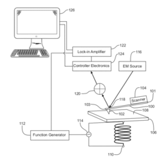
Atomic Force Microscopy System and Method for Nanoscale Measurement
PatentActiveUS20120030846A1
Innovation
- An AFM system with a cantilever and electromagnetic coil that generates a time-varying magnetic field within the sample, allowing for imaging of various properties without bias voltage and using softer cantilevers for higher sensitivity, including electrical, dielectric, and magnetic properties, with a non-magnetic or magnetic tip.
Monitoring changes in supra-cellular structures
PatentWO2012069095A1
Innovation
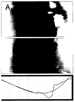
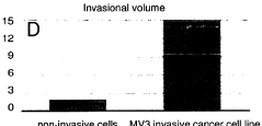
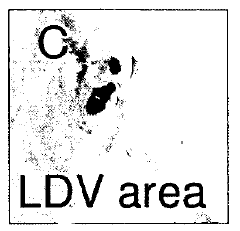
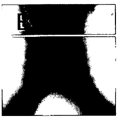
- A method involving atomic force microscopy (AFM) to determine the local deviational volume (LDV) of supra-cellular structures, allowing for the quantification of changes in the meshwork by analyzing topographical elements and comparing them to calibrated samples, enabling the assessment of disease-related changes and invasive potential.
Cost-Benefit Analysis of Microscopy Technologies
When evaluating microscopy technologies for research or industrial applications, a comprehensive cost-benefit analysis is essential to make informed investment decisions. Atomic Force Microscopy (AFM) and Electron Microscopy (EM) represent two distinct approaches with significantly different financial implications and operational considerations.
Initial acquisition costs present the most obvious difference between these technologies. Electron microscopes, particularly Transmission Electron Microscopes (TEM), typically range from $500,000 to several million dollars, while Scanning Electron Microscopes (SEM) generally cost between $250,000 and $1,000,000. In contrast, AFM systems are more accessible, with prices typically between $100,000 and $300,000, making them a more viable option for smaller research institutions or companies with limited capital expenditure budgets.
Operational expenses also differ substantially. Electron microscopes require specialized facilities with electromagnetic shielding, vibration isolation, and often dedicated cooling systems. These infrastructure requirements can add $50,000-$200,000 to the initial setup costs. Additionally, EM systems consume significant electrical power and require regular maintenance contracts costing $20,000-$50,000 annually. AFM systems have more modest facility requirements and lower maintenance costs, typically $5,000-$15,000 annually.
Sample preparation costs represent another important consideration. EM often requires extensive sample preparation including fixation, dehydration, embedding, sectioning, and coating with conductive materials—processes that demand specialized equipment and consumables. AFM sample preparation is generally simpler and less expensive, though still requiring careful handling to achieve optimal results.
Personnel training and expertise requirements also factor into the total cost of ownership. Operating electron microscopes typically requires specialized training that may take months to years to master fully. AFM has a somewhat shorter learning curve, though still requires significant expertise for advanced applications. The salary differential between highly specialized EM technicians versus AFM operators can amount to $10,000-$30,000 annually.
Return on investment considerations must account for throughput capabilities and versatility. While EM systems are more expensive, they often offer higher sample throughput and broader application ranges, potentially serving multiple research groups or industrial applications. AFM systems, though more limited in some applications, excel in others and may provide better value for specific research focuses.
Ultimately, the cost-benefit equation must incorporate both quantitative factors (purchase price, operating costs) and qualitative considerations (research capabilities, resolution requirements, sample compatibility). Organizations must carefully align technology selection with their specific research objectives, budget constraints, and long-term strategic plans to optimize their microscopy investments.
Environmental and Sample Preparation Considerations
Environmental conditions and sample preparation methodologies significantly impact the performance and results obtained from both Atomic Force Microscopy (AFM) and Electron Microscopy (EM). These considerations are crucial for researchers when selecting the appropriate microscopy technique for specific applications.
AFM offers remarkable flexibility regarding environmental conditions. Unlike electron microscopy, AFM can operate in ambient air, liquids, vacuum, and controlled gas environments. This versatility makes AFM particularly valuable for studying biological samples in their native states or for observing dynamic processes in real-time. However, environmental vibrations and acoustic noise can severely compromise AFM measurements, necessitating specialized isolation systems in many laboratory settings.
Sample preparation for AFM is generally less demanding compared to electron microscopy techniques. Many samples can be examined with minimal preparation, often requiring only secure mounting on a flat substrate. This non-destructive approach preserves sample integrity and enables subsequent analyses using complementary techniques. Nevertheless, certain AFM applications may require specific surface treatments to enhance feature contrast or to immobilize biological specimens.
In contrast, electron microscopy techniques impose stringent environmental requirements. Both Scanning Electron Microscopy (SEM) and Transmission Electron Microscopy (TEM) typically operate under high vacuum conditions, which presents significant limitations for hydrated or volatile samples. Environmental SEM (ESEM) partially addresses this limitation by allowing imaging in low-vacuum or controlled humidity environments, though with some resolution compromise.
Sample preparation for electron microscopy is considerably more complex and potentially destructive. For SEM, samples must be electrically conductive or coated with a conductive layer (typically gold or carbon) to prevent charging artifacts. Biological specimens require fixation, dehydration, and critical point drying to maintain structural integrity under vacuum conditions.
TEM sample preparation is even more demanding, requiring ultra-thin sections (typically 50-100 nm) to allow electron transmission. This process involves embedding, sectioning with ultramicrotomes, and often staining with heavy metals to enhance contrast. These extensive preparation procedures can introduce artifacts and potentially alter the native structure of samples.
Temperature control represents another critical consideration, particularly for temperature-sensitive materials or for studying phase transitions. Advanced AFM systems offer precise temperature control capabilities, while maintaining similar capabilities in electron microscopy often requires specialized and expensive equipment.
Unlock deeper insights with Patsnap Eureka Quick Research — get a full tech report to explore trends and direct your research. Try now!
Generate Your Research Report Instantly with AI Agent
Supercharge your innovation with Patsnap Eureka AI Agent Platform!