

Measure Atomic Force Microscopy Scanner Resolution — Standards
SEP 19, 20259 MIN READ
Generate Your Research Report Instantly with AI Agent
PatSnap Eureka helps you evaluate technical feasibility & market potential.
AFM Scanner Resolution Background and Objectives
Atomic Force Microscopy (AFM) has revolutionized nanoscale imaging and measurement since its invention in 1986 by Binnig, Quate, and Gerber. This scanning probe microscopy technique provides three-dimensional surface profiles with nanometer-scale resolution by measuring forces between a sharp probe and sample surface. The scanner resolution represents a fundamental parameter that determines the instrument's capability to distinguish between closely spaced features.
The evolution of AFM scanner technology has progressed from early piezoelectric tube scanners to more sophisticated flexure-based designs. Initial systems offered limited scan ranges and suffered from significant nonlinearities, hysteresis, and creep. Modern scanners incorporate closed-loop control systems with position sensors to mitigate these issues, enabling more precise and reproducible measurements.
Despite these advancements, standardized methods for characterizing AFM scanner resolution remain underdeveloped compared to other microscopy techniques. This gap presents significant challenges for comparing instruments across manufacturers, validating measurement results, and ensuring reliability in critical applications such as semiconductor metrology and nanofabrication.
The primary objective of this technical research is to comprehensively evaluate existing and emerging standards for measuring AFM scanner resolution. This includes examining calibration artifacts, measurement protocols, and mathematical frameworks that quantify lateral and vertical resolution capabilities. The investigation aims to identify best practices that can be universally applied across different AFM platforms and operating modes.
Current standards development efforts by organizations such as ISO, ASTM, and NIST have made progress in establishing calibration procedures for AFM measurements. However, these standards often address specific aspects of AFM operation rather than providing a comprehensive framework for scanner resolution characterization. The ISO/TR 11952:2014 and ASTM E2859 standards represent important steps but require further refinement to address the full complexity of scanner performance.
The technical landscape is further complicated by the diverse operating modes of modern AFMs, including contact, tapping, and non-contact modes, each with distinct resolution limitations. Additionally, environmental factors such as vibration, temperature fluctuations, and acoustic noise significantly impact achievable resolution, necessitating standardized environmental specifications for meaningful comparisons.
This research seeks to bridge the gap between theoretical resolution limits and practical measurement capabilities by developing robust methodologies that account for both instrumental and environmental factors. The ultimate goal is to establish traceable, reproducible standards that enable objective evaluation of AFM scanner resolution across different instruments and operating conditions.
Market Demand Analysis for High-Resolution AFM Standards
The global market for Atomic Force Microscopy (AFM) standards is experiencing robust growth driven by increasing demand for high-precision measurement capabilities across multiple industries. Current market analysis indicates that the AFM standards market is valued at approximately 320 million USD in 2023, with projections suggesting a compound annual growth rate of 6.8% through 2028. This growth trajectory is primarily fueled by expanding applications in semiconductor manufacturing, materials science, and nanotechnology research.
The semiconductor industry represents the largest market segment for high-resolution AFM standards, accounting for roughly 40% of total demand. As semiconductor manufacturers continue to push the boundaries of miniaturization with sub-10nm process nodes becoming standard, the need for precise calibration tools has intensified. Industry reports highlight that over 85% of leading semiconductor fabrication facilities now incorporate AFM measurements as a critical quality control step, creating sustained demand for reliable calibration standards.
Research institutions and academic laboratories constitute the second-largest market segment, representing approximately 30% of the total demand. The increasing focus on nanoscale research across disciplines including physics, chemistry, and biology has elevated the importance of accurate AFM measurements. University research budgets allocated to nanoscale imaging equipment have increased by an average of 12% annually over the past five years, indicating strong institutional commitment to this technology.
Healthcare and life sciences applications are emerging as the fastest-growing segment for AFM standards, with a projected growth rate of 9.3% annually. The application of AFM in pharmaceutical development, particularly for drug delivery systems and protein structure analysis, has created new market opportunities. Additionally, the use of AFM in medical device manufacturing quality control has expanded significantly, with regulatory bodies increasingly requiring nanoscale verification of critical components.
Regional analysis reveals that North America currently leads the market with a 38% share, followed by Europe (31%) and Asia-Pacific (26%). However, the Asia-Pacific region is expected to demonstrate the highest growth rate over the next five years, driven by rapid expansion of semiconductor manufacturing capabilities in Taiwan, South Korea, and China. Government initiatives supporting nanotechnology research in these countries have further stimulated demand for high-precision measurement tools.
Customer surveys indicate that key purchasing factors for AFM standards include measurement accuracy, traceability to international standards, long-term stability, and compatibility with multiple AFM systems. There is particularly strong demand for standards that can verify three-dimensional measurements with sub-nanometer precision, reflecting the increasingly complex structures being analyzed in modern applications.
Current State and Challenges in AFM Resolution Metrology
The field of Atomic Force Microscopy (AFM) resolution metrology currently faces significant challenges despite substantial advancements over the past three decades. While AFM technology has evolved to achieve sub-nanometer resolution capabilities, standardized methods for accurately measuring and verifying this resolution remain inadequately developed. This creates a critical gap between theoretical capabilities and practical verification methodologies.
Current international standards for AFM resolution measurement are fragmented and inconsistent across different regions and applications. The ISO/TC201 committee has established some guidelines, but these often lack specificity for cutting-edge instruments and diverse sample types. This inconsistency makes cross-laboratory comparisons difficult and hampers reliable performance benchmarking in the industry.
A major technical challenge lies in distinguishing between true topographical features and artifacts introduced by the measurement system itself. Tip-sample interactions, environmental vibrations, thermal drift, and electronic noise all contribute to measurement uncertainty. Current calibration artifacts, such as silicon gratings with periodic structures, are insufficient for verifying resolution below 5 nm, where many modern AFM systems claim to operate.
The metrology infrastructure supporting AFM resolution verification is also underdeveloped. Reference materials certified at the sub-nanometer scale are scarce, and those available often suffer from stability issues or manufacturing inconsistencies. National metrology institutes have different approaches to AFM calibration, creating discrepancies in measurement traceability chains.
Software algorithms for resolution determination add another layer of complexity. Various methods—including power spectral density analysis, feature edge detection, and signal-to-noise ratio calculations—yield different resolution values for the same dataset. This algorithmic diversity creates confusion about which method most accurately represents true instrument performance.
The economic impact of these challenges is substantial. Without standardized resolution metrics, manufacturers make performance claims that are difficult to verify independently, creating market inefficiencies and potential misrepresentation of capabilities. End users in critical applications such as semiconductor manufacturing, nanomedicine, and materials science lack reliable methods to validate instrument specifications against their specific requirements.
Geographically, resolution metrology capabilities are concentrated in North America, Western Europe, and East Asia, with significant gaps in other regions. This uneven distribution limits global harmonization efforts and creates barriers to technology transfer and adoption in emerging economies.
Existing Calibration Methods and Reference Materials
01 Scanner design for improved resolution
Various scanner designs can enhance the resolution of atomic force microscopy. These include piezoelectric scanners with optimized geometries, flexure-based mechanisms, and hybrid scanning systems. Advanced scanner designs minimize hysteresis, creep, and thermal drift while providing precise positioning control at the nanoscale. These improvements allow for higher resolution imaging by reducing mechanical noise and increasing stability during scanning operations.- Scanner design for improved resolution: Various scanner designs can enhance the resolution of atomic force microscopy. These include piezoelectric scanners with optimized geometries, flexure-based mechanisms, and hybrid scanner systems that combine coarse and fine positioning capabilities. Advanced scanner designs minimize hysteresis, creep, and thermal drift while providing precise control over the scanning probe, ultimately improving the spatial resolution of AFM measurements.
- Feedback control systems for resolution enhancement: Sophisticated feedback control systems play a crucial role in achieving high-resolution AFM imaging. These systems continuously monitor and adjust the probe-sample interaction forces, maintaining optimal scanning conditions. Advanced algorithms for signal processing, noise reduction, and drift compensation help to stabilize the scanning process and enhance the resolution of the microscope, allowing for more accurate topographical mapping at the nanoscale.
- Probe tip technology for atomic-scale resolution: The design and fabrication of probe tips significantly impact AFM resolution. Ultra-sharp tips with small radii of curvature, often made from materials like silicon, silicon nitride, or functionalized with carbon nanotubes, enable imaging at atomic and molecular scales. Specialized tip treatments and coatings can enhance durability, reduce contamination, and provide specific functionality for different imaging modes, directly affecting the achievable spatial resolution.
- Vibration isolation and environmental control: Environmental factors significantly affect AFM resolution. Advanced vibration isolation systems, including active and passive damping mechanisms, shield the microscope from external mechanical disturbances. Temperature stabilization, acoustic isolation, and electromagnetic shielding further enhance measurement stability. Controlled atmosphere or vacuum environments can eliminate interference from air currents and humidity variations, allowing for sub-nanometer resolution imaging.
- Signal processing and image enhancement techniques: Sophisticated signal processing methods can significantly improve the effective resolution of AFM measurements. These include digital filtering algorithms, noise reduction techniques, and deconvolution methods that compensate for tip-sample convolution effects. Real-time data processing, statistical analysis, and machine learning approaches can extract more information from raw AFM data, enhancing the clarity and resolution of the final images beyond the physical limitations of the scanning system.
02 Feedback control systems for resolution enhancement
Sophisticated feedback control systems are essential for achieving high-resolution AFM imaging. These systems continuously monitor and adjust the probe-sample interaction forces, maintaining optimal scanning conditions. Advanced algorithms compensate for environmental disturbances, scanner nonlinearities, and thermal drift. Closed-loop control systems with high-speed data processing capabilities enable real-time corrections during scanning, resulting in significantly improved spatial resolution and image quality.Expand Specific Solutions03 Probe technology for enhanced resolution
The development of specialized probe technologies has significantly improved AFM resolution capabilities. Ultra-sharp tips with small radii of curvature allow for better interaction with sample surfaces at the atomic scale. Functionalized probes with specific chemical or physical properties enable selective imaging of particular surface features. Carbon nanotube tips and other advanced materials provide exceptional mechanical properties and durability while maintaining high resolution during extended scanning sessions.Expand Specific Solutions04 Vibration isolation and environmental control
Effective vibration isolation systems and environmental controls are crucial for achieving high-resolution AFM imaging. Active and passive damping systems minimize the effects of external vibrations that can degrade image quality. Temperature-controlled enclosures reduce thermal drift and maintain stable operating conditions. Acoustic isolation chambers and electromagnetic shielding further protect the sensitive measurements from environmental disturbances, allowing for atomic-level resolution imaging even in challenging environments.Expand Specific Solutions05 Signal processing and image enhancement techniques
Advanced signal processing and image enhancement techniques play a vital role in improving the effective resolution of AFM systems. Digital filtering algorithms remove noise while preserving important surface features. Deconvolution methods compensate for tip-sample convolution effects that limit resolution. Machine learning approaches can extract additional information from raw data, enhancing subtle features that might otherwise be lost. Real-time data processing enables dynamic adjustment of scanning parameters to optimize resolution for specific sample characteristics.Expand Specific Solutions
Key Players in AFM Instrumentation and Metrology Standards
The Atomic Force Microscopy (AFM) scanner resolution standards market is in a mature growth phase, with established measurement protocols and increasing demand for nanoscale precision. The global AFM market is valued at approximately $500 million, growing steadily at 5-7% annually as nanotechnology applications expand across industries. Leading companies like Bruker Nano, Oxford Instruments Asylum Research, and Keysight Technologies dominate the commercial landscape with high-precision instruments, while research institutions including CNRS, University of California, and Chinese universities (Zhejiang, Harbin Institute of Technology) drive innovation in standardization methods. Japanese manufacturers (Olympus, Hitachi, JEOL) contribute significant technological advancements, creating a competitive ecosystem balancing commercial solutions with academic research to address increasing demands for quantifiable nanoscale measurements.
Bruker Nano, Inc.
Technical Solution: Bruker Nano has developed comprehensive AFM scanner resolution standards and calibration methods. Their approach includes the use of precision-engineered calibration gratings with known dimensions and patterns that allow for accurate X, Y, and Z calibration. Bruker's technology incorporates closed-loop scanner systems with position sensors that provide real-time feedback on scanner position, significantly reducing nonlinearity, hysteresis, and creep effects that can compromise measurement accuracy. Their latest systems feature advanced piezoelectric scanners with sub-nanometer resolution capabilities and thermal stability controls to minimize drift during high-precision measurements. Bruker has also developed specialized software algorithms for scanner calibration that compensate for inherent scanner nonlinearities and environmental factors affecting measurement accuracy.
Strengths: Industry-leading precision with documented sub-angstrom resolution capabilities; comprehensive calibration solutions covering all axes; advanced software compensation algorithms. Weaknesses: Premium pricing structure; proprietary calibration standards may limit interoperability with other systems; complex calibration procedures require specialized training.
Oxford Instruments Asylum Research, Inc.
Technical Solution: Oxford Instruments Asylum Research has pioneered innovative approaches to AFM scanner resolution standardization through their Cypher and Jupiter AFM systems. Their technology implements sensor-based closed-loop scanning with advanced digital controllers that achieve picometer-level positioning accuracy. Asylum's approach includes proprietary calibration routines using precision-manufactured silicon gratings with features traceable to international standards. Their systems incorporate active thermal management to minimize drift, crucial for maintaining calibration accuracy during high-resolution imaging. Asylum Research has developed BlueDrive photothermal excitation technology that improves measurement reliability by providing pure, stable cantilever excitation without introducing artifacts that could affect scanner calibration. Their scanner designs feature flexure-based mechanisms that eliminate out-of-plane motion and minimize cross-coupling between axes, ensuring more accurate dimensional measurements.
Strengths: Exceptional thermal stability for drift-free measurements; advanced closed-loop control systems; innovative photothermal excitation technology improves measurement reliability. Weaknesses: Higher cost compared to basic AFM systems; specialized calibration procedures may require factory service; limited compatibility with third-party calibration standards.
Critical Technologies for AFM Resolution Measurement
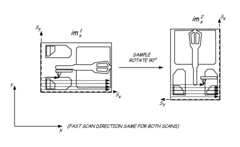
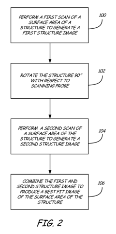
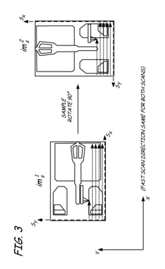
Atomic force microscopy true shape measurement method
PatentInactiveUS8296860B2
Innovation
- The method involves scanning a structure and a flat standard surface twice, each time rotated 90°, and combining the images to produce best fit images. These best fit images are then subtracted to eliminate thermal drift and Zrr errors, allowing for the generation of a true topographical image.
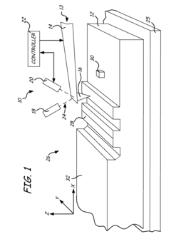
Sample holder for holding samples at pre-determined angles
PatentInactiveUS20090145247A1
Innovation
- A sample holder with multiple inclined regions allows precise placement of test samples at predefined angles, enabling accurate characterization of AFMs by facilitating multiple linearity measurements without the need for additional attachment devices.


International Standards and Certification Requirements
The standardization landscape for Atomic Force Microscopy (AFM) scanner resolution measurement is governed by several key international bodies. ISO (International Organization for Standardization) has developed specific standards including ISO 11039 and ISO 11775, which establish methodologies for calibrating and verifying AFM scanner performance. These standards define reference materials, measurement protocols, and uncertainty calculation methods essential for ensuring consistent resolution measurements across different instruments and laboratories.
ASTM International complements these efforts with standards such as ASTM E2530, which provides guidelines for reporting AFM data and specifies minimum requirements for resolution verification. The National Institute of Standards and Technology (NIST) in the United States has developed certified reference materials specifically designed for AFM calibration, including the SRM 2090 series featuring precisely engineered step heights and pitch patterns.
European certification frameworks, particularly those established by the European Committee for Standardization (CEN), require AFM manufacturers to demonstrate compliance with resolution specifications through standardized testing procedures. These requirements are increasingly being harmonized with global standards to facilitate international trade and research collaboration in nanotechnology.
Certification processes typically involve third-party verification using traceable standards and documented measurement uncertainty. Manufacturers seeking certification must demonstrate that their AFM scanners can resolve features at claimed resolutions under specified environmental conditions. This process includes rigorous testing against calibration artifacts with known dimensions traceable to national metrology institutes.
The International Bureau of Weights and Measures (BIPM) coordinates international comparisons between national metrology institutes to ensure global consistency in nanoscale measurements. These comparisons establish equivalence between different national standards and support mutual recognition of calibration certificates across borders.
Recent developments in standardization include the incorporation of machine learning algorithms for automated resolution assessment and the establishment of round-robin testing protocols among reference laboratories. These advances aim to address the challenges of measuring resolution at the atomic scale, where thermal drift, vibration, and tip-sample interactions can significantly impact measurement accuracy.
Compliance with these international standards is increasingly becoming a market requirement, particularly for AFM systems used in regulated industries such as semiconductor manufacturing, pharmaceutical research, and medical device development. Manufacturers who can demonstrate adherence to these standards gain competitive advantages through enhanced credibility and access to quality-conscious market segments.
Uncertainty Analysis and Traceability in AFM Measurements
Uncertainty analysis in Atomic Force Microscopy (AFM) measurements represents a critical aspect of ensuring reliable and reproducible results. The complex nature of AFM systems introduces multiple sources of uncertainty that must be systematically identified, quantified, and managed to establish measurement traceability.
Primary uncertainty sources in AFM measurements include thermal drift, piezoelectric creep, hysteresis, non-linearity in scanner movement, and environmental factors such as vibration, temperature fluctuations, and humidity. These factors collectively impact the accuracy and precision of scanner resolution measurements, necessitating comprehensive uncertainty budgeting approaches.
Metrological traceability in AFM measurements requires establishing an unbroken chain of calibrations to internationally recognized standards. This typically involves calibration against certified reference materials (CRMs) such as step height standards, calibration gratings, or atomic lattice structures with known dimensions. The National Metrology Institutes (NMIs) like NIST (USA), PTB (Germany), and NPL (UK) have developed specialized standards specifically for AFM calibration.
Statistical methods play a crucial role in uncertainty analysis, including Type A evaluation (based on statistical analysis of series of observations) and Type B evaluation (based on scientific judgment using available information). The combined standard uncertainty is typically calculated using the law of propagation of uncertainties, considering both random and systematic error components.
International standards such as ISO 11039 and ISO 27911 provide frameworks for uncertainty evaluation in AFM measurements. These standards outline procedures for scanner calibration, performance verification, and uncertainty reporting, ensuring consistency across different laboratories and measurement conditions.
Advanced computational approaches have emerged to enhance uncertainty analysis, including Monte Carlo simulations that model the propagation of distributions through complex measurement equations. These methods are particularly valuable for non-linear measurement systems like AFM scanners where traditional uncertainty propagation formulas may be inadequate.
Establishing traceability requires periodic verification against reference standards, with calibration intervals determined based on stability analysis of the AFM system. Documentation of calibration procedures, environmental conditions, and uncertainty calculations forms an essential component of the traceability chain, enabling reproducibility and comparability of measurements across different instruments and laboratories.
Unlock deeper insights with PatSnap Eureka Quick Research — get a full tech report to explore trends and direct your research. Try now!
Generate Your Research Report Instantly with AI Agent
Supercharge your innovation with PatSnap Eureka AI Agent Platform!