

Measure Atomic Force Microscopy Scanning Speed — Evaluation Techniques
SEP 19, 20259 MIN READ
Generate Your Research Report Instantly with AI Agent
PatSnap Eureka helps you evaluate technical feasibility & market potential.
AFM Scanning Speed Evolution and Objectives
Atomic Force Microscopy (AFM) has undergone significant evolution since its invention in 1986 by Gerd Binnig, Calvin Quate, and Christoph Gerber. Initially, AFM scanning speeds were extremely limited, with typical image acquisition times ranging from 30 minutes to several hours for a single high-resolution image. This limitation severely restricted the application scope of AFM technology, particularly for time-sensitive processes and dynamic surface phenomena.
The progression of AFM scanning speeds can be traced through several distinct technological generations. First-generation AFMs (1986-1995) operated at speeds of approximately 0.1-1 Hz per line, resulting in imaging times of hours for detailed surface characterization. The second generation (1995-2005) saw improvements through enhanced feedback electronics and optimized probe designs, pushing scanning speeds to 1-10 Hz per line.
A significant breakthrough occurred with the introduction of high-speed AFM (HS-AFM) around 2008, pioneered by Toshio Ando's group, which enabled video-rate imaging at speeds exceeding 10 frames per second. This represented a paradigm shift in AFM capabilities, allowing for real-time observation of biomolecular processes and dynamic surface interactions previously impossible to capture.
The primary technical objectives driving AFM scanning speed advancements include reducing mechanical resonances in the scanning system, developing faster and more responsive feedback control algorithms, and creating smaller cantilevers with higher resonance frequencies. These improvements aim to overcome the fundamental speed limitations imposed by the mechanical nature of the scanning process while maintaining nanometer-scale resolution.
Current state-of-the-art commercial systems can achieve line rates of 10-100 Hz, with specialized research instruments pushing beyond 1000 Hz. However, these advances often involve trade-offs between speed, resolution, and scan area size. The relationship between these parameters follows approximately a cubic relationship, where doubling the scan speed typically reduces the possible scan area by a factor of eight for equivalent image quality.
Looking forward, the field is targeting several ambitious objectives: achieving video-rate imaging (>30 frames per second) for standard sample types, developing robust methods for quantitative performance evaluation across different AFM platforms, and creating adaptive scanning algorithms that optimize speed based on sample characteristics. These goals are driven by emerging applications in fields such as semiconductor manufacturing, where in-line metrology requires both high throughput and precision, and in biological sciences, where capturing transient cellular processes demands unprecedented temporal resolution.
Market Demand Analysis for High-Speed AFM
The global market for High-Speed Atomic Force Microscopy (HS-AFM) has witnessed significant growth in recent years, driven primarily by increasing demands in nanoscience research, materials science, and biological applications. The traditional AFM technology, while powerful for nanoscale imaging, has been limited by its slow scanning speeds, typically taking minutes to hours to generate a single image. This limitation has created a substantial market gap for technologies that can perform real-time observations of dynamic processes at the nanoscale.
Market research indicates that the overall AFM market was valued at approximately $570 million in 2022, with high-speed variants representing a rapidly growing segment projected to expand at a CAGR of 6.8% through 2028. This growth is particularly pronounced in the life sciences sector, where researchers require tools capable of observing biomolecular interactions and cellular processes in real-time.
The pharmaceutical and biotechnology industries have emerged as major drivers for HS-AFM adoption, as these sectors increasingly rely on nanoscale analysis for drug development and quality control processes. The ability to observe protein dynamics, enzyme activities, and molecular binding events in real-time provides invaluable insights that were previously unattainable with conventional microscopy techniques.
Academic and research institutions constitute another significant market segment, accounting for over 40% of the current HS-AFM installations worldwide. The demand in this sector is fueled by research grants focused on nanoscience and the growing emphasis on interdisciplinary research that bridges physics, chemistry, and biology at the nanoscale.
Geographically, North America and Europe currently dominate the market, collectively accounting for approximately 65% of global HS-AFM sales. However, the Asia-Pacific region, particularly Japan, China, and South Korea, is experiencing the fastest growth rate, driven by substantial government investments in nanotechnology research infrastructure.
Industry surveys reveal that end-users are primarily concerned with three key performance metrics when evaluating HS-AFM systems: temporal resolution (frames per second), spatial resolution (ability to resolve nanoscale features while scanning rapidly), and sample compatibility (ability to image diverse sample types without damage). These metrics directly relate to scanning speed evaluation techniques, highlighting the critical importance of standardized methods for measuring and comparing AFM scanning speeds across different systems.
The market analysis also indicates a growing demand for integrated solutions that combine high-speed AFM capabilities with complementary techniques such as optical microscopy, Raman spectroscopy, or electrical measurements. This trend reflects the evolving needs of researchers who require multimodal characterization of nanoscale phenomena.
Current Limitations in AFM Scanning Velocity
Despite significant advancements in Atomic Force Microscopy (AFM) technology over the past three decades, scanning speed remains a critical bottleneck that limits broader industrial applications. Current commercial AFM systems typically operate at scan rates between 0.1-10 Hz per line, resulting in image acquisition times ranging from several minutes to hours for high-resolution imaging. This temporal limitation severely restricts the ability to observe dynamic processes at the nanoscale and reduces throughput for industrial quality control applications.
The fundamental physical constraints limiting AFM scanning velocity stem from the mechanical properties of the cantilever-based sensing mechanism. Conventional cantilevers exhibit resonance frequencies in the 10-500 kHz range, which inherently caps the mechanical bandwidth of the system. When scan speeds exceed certain thresholds relative to these resonance characteristics, the cantilever cannot accurately track the sample topography, resulting in significant image distortions and measurement artifacts.
Feedback loop performance presents another major limitation. Traditional proportional-integral-derivative (PID) control systems struggle to maintain stable tip-sample interactions at high scan rates. The feedback bandwidth typically ranges from 5-30 kHz in commercial systems, creating a practical ceiling for scanning speeds. When this bandwidth is exceeded, the controller cannot respond quickly enough to topographical changes, leading to tip-sample force variations that compromise measurement accuracy and potentially damage both the tip and sample.
Piezoelectric actuator limitations further constrain scanning velocity. These actuators, which provide the precise positioning necessary for AFM operation, suffer from inherent hysteresis, creep, and non-linearity that become more pronounced at higher scan rates. Additionally, their mechanical resonances (typically in the 1-10 kHz range for conventional scanners) introduce unwanted oscillations and positioning errors when excited by rapid scanning movements.
Environmental factors also impose practical limits on scanning speed. Acoustic vibrations, thermal drift, and electromagnetic interference become increasingly problematic as scan rates increase, degrading signal-to-noise ratios and measurement precision. These effects are particularly challenging in ambient conditions where environmental control is limited.
Data acquisition and processing capabilities represent another bottleneck. High-speed scanning generates enormous data volumes that strain the capabilities of current data acquisition systems, which typically operate at sampling rates of 100 kHz to 5 MHz. Real-time processing of this data stream becomes computationally intensive, often requiring specialized hardware and optimized algorithms to maintain measurement fidelity at elevated scan rates.
Existing Measurement Methodologies
01 High-speed scanning techniques in AFM
Advanced techniques for increasing the scanning speed of atomic force microscopy without compromising image quality. These include optimized feedback control systems, improved scanner designs, and specialized algorithms that allow for faster data acquisition while maintaining resolution. High-speed AFM enables real-time observation of dynamic processes at the nanoscale that would be impossible to capture with conventional scanning speeds.- High-speed scanning techniques for AFM: Various techniques have been developed to increase the scanning speed of atomic force microscopy without compromising image quality. These include optimized feedback control systems, advanced piezoelectric actuators, and specialized scanning algorithms that reduce mechanical resonances. High-speed AFM enables real-time observation of dynamic biological processes and nanoscale phenomena that occur on millisecond timescales.
- Mechanical design improvements for faster scanning: Innovations in the mechanical design of AFM components significantly impact scanning speed. These include lightweight cantilevers with high resonance frequencies, optimized scanner geometries that minimize mass and increase stiffness, and improved damping systems that reduce vibration. Such mechanical enhancements allow for faster tip movement while maintaining precise control over the scanning process.
- Advanced control systems for AFM scanning: Sophisticated control systems play a crucial role in enhancing AFM scanning speed. These include adaptive feedback controllers, model-based predictive control algorithms, and digital signal processing techniques that compensate for scanner nonlinearities and hysteresis. Such control systems enable faster response times and more accurate tracking of sample topography at increased scanning rates.
- Multifrequency and parallel scanning approaches: Novel approaches to increase effective scanning speed include multifrequency excitation techniques, where multiple cantilever resonance modes are simultaneously excited and detected, and parallel scanning systems that employ multiple tips operating concurrently. These methods significantly increase data acquisition rates and enable faster imaging of large sample areas without sacrificing resolution.
- Sample preparation and environmental factors affecting scanning speed: Sample preparation techniques and environmental conditions significantly impact achievable scanning speeds in AFM. Factors such as sample stiffness, adhesion properties, surface roughness, and imaging medium (air, liquid, vacuum) all affect the maximum possible scanning rate. Optimizing these factors through specialized sample preparation protocols and environmental control systems can enable faster scanning while maintaining image quality.
02 Resonance compensation for AFM scanners
Methods to compensate for mechanical resonances that limit scanning speed in atomic force microscopes. These approaches involve active damping techniques, mechanical design modifications to increase resonant frequencies, and advanced control algorithms that can operate beyond the first resonance of the scanner. By addressing resonance issues, these innovations allow for significantly faster scanning while maintaining accurate topographical measurements.Expand Specific Solutions03 Multifrequency and parallel scanning methods
Innovative approaches that utilize multiple frequencies or parallel probes to increase the effective scanning speed of atomic force microscopy. These techniques allow simultaneous acquisition of different sample properties or multiple sample areas, effectively multiplying the data collection rate. Implementation includes specialized probe arrays, multiplexed detection systems, and advanced signal processing algorithms to handle the increased data throughput.Expand Specific Solutions04 Feedback optimization for faster scanning
Specialized feedback control systems designed to optimize the scanning speed in atomic force microscopy. These systems include adaptive controllers that adjust parameters in real-time, predictive algorithms that anticipate surface features, and hybrid control schemes that combine multiple feedback mechanisms. By reducing the response time of the feedback loop while maintaining stable tip-sample interaction, these innovations enable faster scanning without sacrificing measurement accuracy.Expand Specific Solutions05 Novel scanner designs for high-speed AFM
Innovative mechanical designs of scanners specifically engineered to achieve higher scanning speeds in atomic force microscopy. These include miniaturized scanners with reduced moving mass, counterbalanced designs to minimize unwanted vibrations, and scanners made from materials with optimized mechanical properties. The novel designs focus on increasing resonant frequencies and reducing settling times to enable faster image acquisition without introducing artifacts.Expand Specific Solutions
Leading Manufacturers and Research Institutions
The Atomic Force Microscopy (AFM) scanning speed measurement market is in a growth phase, with increasing demand for high-throughput metrology solutions in semiconductor manufacturing and materials research. The competitive landscape features established scientific instrument manufacturers like Bruker Nano, Hitachi, and Agilent Technologies alongside specialized AFM innovators such as Infinitesima and Nearfield Instruments. Academic institutions including Beihang University, Zhejiang University, and IMEC are advancing fundamental research in this field. Technology maturity varies significantly, with traditional AFM companies offering reliable but slower solutions, while newer entrants like Infinitesima with their Rapid Probe Microscopy technology are pushing scanning speed boundaries. The market is evolving toward faster, more precise measurement techniques to meet semiconductor industry demands for atomic-scale metrology at production-relevant throughput.
Bruker Nano, Inc.
Technical Solution: Bruker Nano has developed advanced high-speed atomic force microscopy (AFM) scanning technologies through their FastScan and PeakForce Tapping modes. Their evaluation techniques for measuring AFM scanning speed include real-time error signal monitoring systems that quantify the accuracy of the probe tracking during high-speed operations. Bruker's proprietary algorithms automatically adjust scanning parameters based on sample topography to maintain optimal imaging quality while maximizing speed. Their systems incorporate specialized high-bandwidth electronics and low-noise detection systems capable of accurately measuring cantilever deflection at scan rates exceeding 125 Hz. For evaluation, they employ comparative analysis frameworks that measure signal-to-noise ratios across different scanning speeds to determine the optimal speed-to-quality ratio for specific applications. Bruker's PeakForce Tapping technology enables force curve acquisition at each pixel with rates up to 8 kHz, allowing for simultaneous mechanical property mapping during high-speed topographical imaging.
Strengths: Industry-leading scan rates with minimal image distortion; comprehensive evaluation metrics that consider both speed and data quality; integrated calibration systems for accurate force measurements at high speeds. Weaknesses: Premium pricing structure limits accessibility; requires specialized training for optimal performance; some high-speed modes may introduce artifacts in certain sample types.
Infinitesima Ltd.
Technical Solution: Infinitesima has pioneered the Rapid Probe Microscopy (RPM) technology specifically designed to address high-speed AFM scanning challenges. Their evaluation methodology centers on their patented resonating probe technology that operates at frequencies significantly higher than conventional AFM systems. The company's approach includes specialized metrics for quantifying scanning speed performance, including their "effective pixel acquisition rate" which measures the number of accurate data points collected per second. Their RPM technology achieves scanning speeds up to 100 times faster than traditional AFM systems by employing a unique scanning mechanism that eliminates many of the mechanical limitations of conventional piezoelectric scanners. For evaluation, Infinitesima utilizes comparative image quality assessment at varying scan rates, with proprietary algorithms that analyze topographical accuracy, feature resolution, and signal noise as functions of scanning speed. Their systems incorporate real-time feedback mechanisms that continuously optimize scanning parameters to maintain data integrity at maximum possible speeds.
Strengths: Revolutionary scanning mechanism enabling exceptionally high throughput; specialized for semiconductor inspection applications; comprehensive speed evaluation metrics integrated into system software. Weaknesses: More specialized for industrial applications rather than research flexibility; limited availability of compatible probes compared to conventional systems; higher initial investment costs.
Key Patents in AFM Speed Evaluation
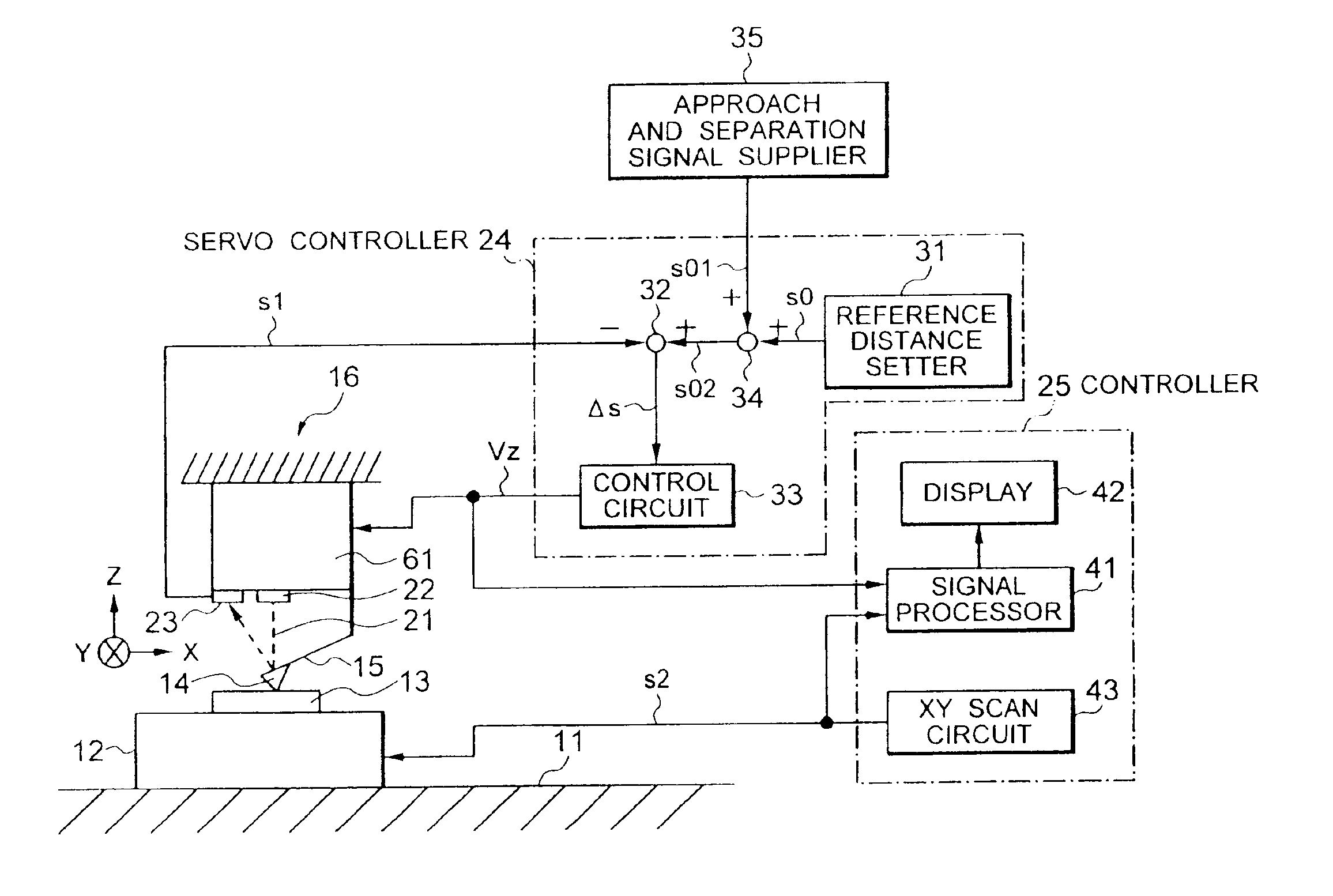
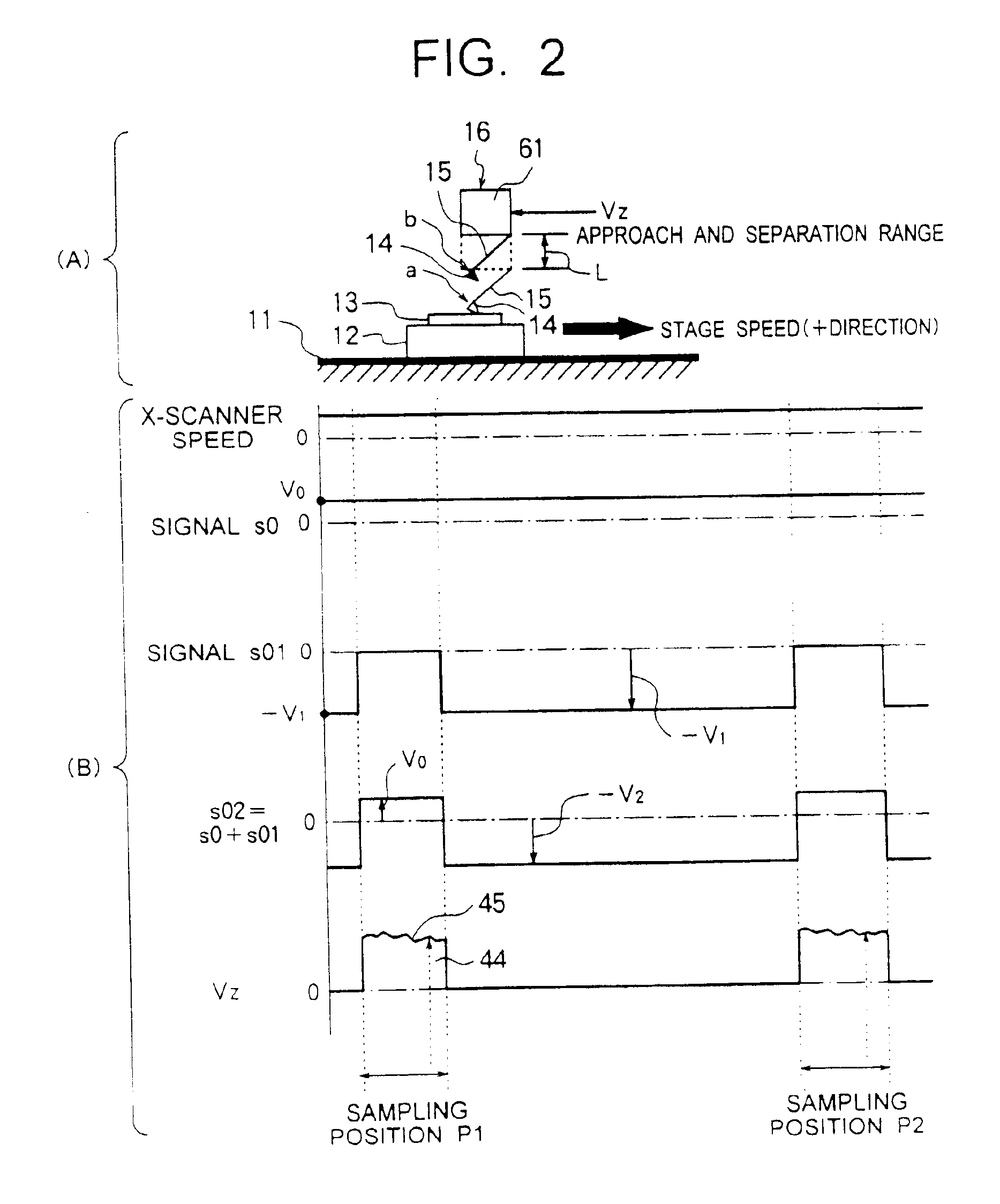
Scanning probe microscope and method of measurement
PatentInactiveUS6881954B1
Innovation
- A scanning probe microscope configuration that maintains servo control during probe approach and separation, utilizing a cantilever with a piezoelectric actuator and light lever photo detection for displacement measurement, allows for precise control of the probe's distance from the sample surface, reducing the impact of frictional forces and adsorption layer variations, and incorporating an auxiliary movement mechanism for tandem scanning to prevent parallel forces.

Fast image scanning method for the operation of atomic force microscope under liquid conditions
PatentActiveKR1020100092990A
Innovation
- A method for calculating Fnet_2 and Vy values using equations to determine optimal scan rates for atomic force microscopy in liquid phase, adjusting variables to minimize image distortion without additional equipment, applicable to all commercially manufactured AFMs.


Calibration Standards and Protocols
Standardized calibration protocols are essential for ensuring the reliability and reproducibility of Atomic Force Microscopy (AFM) scanning speed measurements. The development of universally accepted calibration standards has significantly advanced the field by providing researchers with consistent benchmarks against which to evaluate their systems. These standards typically include reference samples with well-characterized features at multiple length scales, allowing for comprehensive validation of scanning performance across different operational parameters.
Primary calibration standards for AFM scanning speed evaluation include silicon gratings with precisely defined pitch values, typically ranging from 1 μm to 10 μm. These gratings enable the assessment of both lateral and vertical calibration accuracy at various scanning speeds. Additionally, specialized dynamic calibration samples featuring oscillating structures have been developed specifically for high-speed AFM applications, providing a means to evaluate the system's response to rapidly changing topographical features.
International metrology organizations, including the National Institute of Standards and Technology (NIST) and the International Organization for Standardization (ISO), have established standardized protocols for AFM calibration procedures. ISO/TR 11952:2014 specifically addresses calibration methodologies for scanning probe microscopes, providing guidelines for speed-dependent measurements. These protocols typically require multiple measurements at incrementally increasing scan rates to establish speed-dependent correction factors and uncertainty values.
Calibration procedures must account for the non-linear behavior of piezoelectric scanners at different scanning speeds. This includes hysteresis effects, creep, and thermal drift, all of which can significantly impact measurement accuracy. Modern calibration protocols incorporate compensation algorithms that adjust for these non-linearities based on empirical measurements of standard reference materials.
Traceability to SI units remains a fundamental requirement for AFM calibration standards. This is typically achieved through comparison with measurements obtained via other metrology techniques such as optical interferometry or electron microscopy. The uncertainty budget for scanning speed calibration must include contributions from the reference standard's certification, the measurement procedure, environmental conditions, and instrument-specific factors.
Regular recalibration schedules are recommended as part of standard operating procedures, with frequency determined by usage patterns and environmental stability. Documentation of calibration history provides valuable data for long-term performance monitoring and can reveal gradual changes in scanner behavior that might otherwise go unnoticed. This systematic approach to calibration ensures that scanning speed measurements remain reliable and comparable across different instruments and laboratories.
Real-time Data Processing Challenges
Real-time data processing represents one of the most significant challenges in advancing Atomic Force Microscopy (AFM) scanning speeds. As AFM technology evolves toward faster acquisition rates, the computational infrastructure supporting these systems faces increasing demands that test the limits of current processing capabilities.
The primary challenge stems from the massive data throughput generated during high-speed AFM scanning. Modern high-speed AFMs can generate data at rates exceeding 100 MB/s, creating substantial computational bottlenecks. This data flood requires not only sufficient bandwidth for transfer but also processing power capable of handling complex operations on these datasets without introducing latency.
Signal-to-noise ratio degradation presents another critical challenge in real-time processing. As scanning speeds increase, the signal quality typically decreases, necessitating more sophisticated filtering and enhancement algorithms. These algorithms must operate within microsecond timeframes to maintain the real-time nature of the system, placing extraordinary demands on processing hardware.
Feedback loop responsiveness represents a fundamental limitation in current systems. The control mechanisms that maintain tip-sample interactions require near-instantaneous processing to adjust parameters based on incoming data. Any delay in this processing chain directly impacts scanning accuracy and resolution, particularly at higher speeds where mechanical resonances and other artifacts become more pronounced.
Hardware limitations further constrain real-time processing capabilities. While FPGA-based solutions offer promising performance for specific processing tasks, they lack the flexibility of software-based approaches. GPU acceleration provides computational power but introduces data transfer overhead that can negate speed advantages in certain scenarios.
Memory management becomes increasingly critical as scan speeds rise. Buffer overflows and data handling inefficiencies can introduce artifacts or data loss that compromise measurement integrity. Systems must implement sophisticated memory allocation strategies to ensure continuous data flow without interruption.
The integration of machine learning algorithms for real-time feature recognition and artifact correction represents both an opportunity and a challenge. While these approaches show promise for enhancing data quality during high-speed scanning, they introduce additional computational complexity that must be balanced against processing time constraints.
Future advances in real-time processing for AFM will likely require heterogeneous computing architectures that combine specialized hardware accelerators with flexible software frameworks, potentially leveraging edge computing paradigms to distribute processing loads more effectively across the system architecture.
Unlock deeper insights with PatSnap Eureka Quick Research — get a full tech report to explore trends and direct your research. Try now!
Generate Your Research Report Instantly with AI Agent
Supercharge your innovation with PatSnap Eureka AI Agent Platform!