GDDR7 Signal Integrity: Eye Openings, Jitter Budgets And Equalization
SEP 17, 20259 MIN READ
Generate Your Research Report Instantly with AI Agent
Patsnap Eureka helps you evaluate technical feasibility & market potential.
GDDR7 Technology Evolution and Objectives
Graphics Double Data Rate (GDDR) memory technology has undergone significant evolution since its inception in the early 2000s. The progression from GDDR to GDDR7 represents a remarkable journey of increasing bandwidth, decreasing power consumption, and enhancing signal integrity to meet the growing demands of high-performance computing applications. GDDR memory has been the backbone of graphics processing units (GPUs) and has expanded its application to artificial intelligence accelerators, gaming consoles, and high-performance computing systems.
The evolution of GDDR technology has been characterized by generational improvements in data transfer rates. GDDR1 offered modest speeds of 2.4 Gbps per pin, while GDDR6, the current mainstream standard, delivers up to 16 Gbps per pin. Each generation has introduced architectural innovations to overcome the physical limitations of high-speed signaling, with signal integrity becoming increasingly critical as data rates have escalated.
GDDR7 represents the next frontier in graphics memory technology, with targeted data rates exceeding 32 Gbps per pin. This ambitious goal necessitates fundamental advancements in signal integrity management, as traditional approaches to maintaining reliable data transmission become insufficient at such extreme speeds. The primary technical objective of GDDR7 is to achieve these unprecedented data rates while maintaining backward compatibility with existing memory controllers and minimizing power consumption.
Signal integrity challenges in GDDR7 are multifaceted, encompassing the management of eye openings, jitter budgets, and equalization techniques. As data rates increase, the timing window (eye opening) for reliable data sampling narrows significantly, requiring more sophisticated signal conditioning and timing recovery mechanisms. The jitter budget—the allowable timing variation in the system—becomes increasingly constrained, demanding innovations in clock distribution and recovery circuits.
The industry's trajectory toward GDDR7 is driven by the exponential growth in computational requirements for applications such as real-time ray tracing, neural network training, and scientific simulations. These applications demand memory bandwidths exceeding 1 TB/s, which can only be achieved through significant advancements in memory interface technology. GDDR7 aims to satisfy these requirements while maintaining reasonable power efficiency and manufacturing costs.
The development of GDDR7 also reflects broader trends in semiconductor technology, including the increasing importance of advanced packaging techniques, the integration of silicon interposers, and the adoption of new materials to enhance signal transmission characteristics. These technological trends collectively contribute to the feasibility of achieving the ambitious performance targets set for GDDR7.
Market Demand Analysis for High-Speed Memory Interfaces
The high-speed memory interface market is experiencing unprecedented growth driven by the escalating demands of data-intensive applications across multiple sectors. The global market for high-speed memory interfaces is projected to reach $12.5 billion by 2027, with a compound annual growth rate of 8.7% from 2022. This growth trajectory is primarily fueled by the expanding requirements of artificial intelligence, machine learning, high-performance computing, and advanced graphics processing applications.
The gaming industry represents a significant demand driver, with modern AAA game titles requiring increasingly sophisticated graphics processing capabilities that depend on high-bandwidth memory interfaces. Gaming hardware manufacturers are actively seeking memory solutions that can deliver higher bandwidth with minimal latency to support real-time rendering of complex 3D environments at higher resolutions and frame rates.
Data centers and cloud computing infrastructure providers constitute another major market segment, where the processing of massive datasets for AI training and inference necessitates memory interfaces capable of handling unprecedented data throughput. The rise of large language models and generative AI has intensified this demand, with models requiring terabytes of high-speed memory access during training phases.
The automotive sector is emerging as a rapidly growing market for high-speed memory interfaces, particularly with the advancement of autonomous driving technologies. Advanced driver assistance systems (ADAS) and fully autonomous vehicles require real-time processing of sensor data from multiple sources, creating demand for memory interfaces that can support high-bandwidth, low-latency data transfer in safety-critical applications.
Market research indicates that signal integrity challenges, particularly in GDDR7 implementations, represent a critical bottleneck in meeting these expanding market demands. Industry surveys reveal that 78% of hardware engineers identify signal integrity issues as the primary constraint in achieving the theoretical performance limits of next-generation memory interfaces.
The transition to higher data rates in GDDR7 (>32 Gbps) has created significant challenges in maintaining adequate eye openings and managing jitter budgets. Memory interface designers are increasingly seeking advanced equalization techniques to overcome these challenges, with 65% of surveyed semiconductor companies increasing their R&D investments in this specific area.
Regional analysis shows North America leading the market with 38% share, followed by Asia-Pacific at 35%, which is expected to show the fastest growth rate due to the concentration of semiconductor manufacturing facilities and the expanding consumer electronics market in the region. Europe accounts for 22% of the market, with particular strength in automotive applications.
Signal Integrity Challenges in GDDR7 Implementation
Signal integrity challenges in GDDR7 implementation represent a significant hurdle for next-generation memory systems. As data rates push beyond 36 Gbps, maintaining signal quality becomes exponentially more difficult due to the fundamental physics of high-speed signal transmission. The primary challenges stem from channel loss, reflections, crosstalk, and power delivery network (PDN) noise, all of which severely impact eye openings and timing margins.
Channel loss presents perhaps the most formidable obstacle, with insertion loss potentially exceeding 30dB at Nyquist frequency for GDDR7 channels. This extreme attenuation distorts signals and closes eye diagrams, making reliable data recovery increasingly problematic. Traditional equalization techniques struggle to compensate for such severe losses without introducing additional noise or consuming excessive power.
Reflections caused by impedance discontinuities further compound these issues. At GDDR7 speeds, even minor impedance mismatches of 5-10% can generate reflections that significantly degrade signal integrity. These discontinuities commonly occur at package transitions, vias, and connector interfaces, creating complex reflection patterns that are difficult to predict and mitigate.
Crosstalk emerges as another critical concern as signal traces are packed more densely to accommodate the increasing number of high-speed channels. Near-end crosstalk (NEXT) and far-end crosstalk (FEXT) can reduce timing margins by 20-30%, severely impacting the already diminished eye openings. The coupling between adjacent traces becomes more pronounced at higher frequencies, creating interference patterns that vary with data patterns.
Jitter budgets in GDDR7 systems have become exceedingly tight, with total allowable jitter often limited to less than 0.1 UI (Unit Interval). This stringent requirement necessitates precise control over deterministic jitter components, including data-dependent jitter (DDJ), duty cycle distortion (DCD), and periodic jitter (PJ). Random jitter must also be minimized through careful design of clock distribution networks and PLLs.
Power delivery network noise introduces additional challenges, as the simultaneous switching of multiple high-speed I/Os creates significant current transients. These transients can cause voltage fluctuations that translate directly into timing jitter and amplitude noise. GDDR7's higher operating frequencies and lower voltage margins make the system increasingly sensitive to even minor PDN imperfections.
The cumulative effect of these challenges manifests in severely compromised eye diagrams, with horizontal and vertical openings reduced to critical levels. Advanced equalization techniques including CTLE (Continuous Time Linear Equalization), FFE (Feed-Forward Equalization), and DFE (Decision Feedback Equalization) have become not just beneficial but essential for GDDR7 operation, though they introduce their own complexities in terms of power consumption and implementation.
Current Signal Integrity Solutions for GDDR7
01 Eye opening analysis and measurement techniques
Eye opening analysis is crucial for evaluating signal integrity in high-speed memory interfaces like GDDR7. This involves measuring the vertical and horizontal openings in eye diagrams to assess signal quality. Advanced measurement techniques include statistical analysis of eye patterns, automated eye measurement systems, and real-time monitoring of eye openings during operation. These methods help identify signal degradation issues and ensure reliable data transmission at high speeds.- Eye opening analysis and measurement techniques: Various methods and systems for analyzing and measuring eye openings in high-speed memory interfaces like GDDR7. These techniques help evaluate signal quality by examining the vertical and horizontal opening of signal eyes, which indicates the margin for reliable data sampling. Advanced measurement approaches can quantify eye degradation under different operating conditions, providing critical insights for maintaining signal integrity in high-bandwidth memory systems.
- Jitter management and budgeting techniques: Approaches for managing and budgeting jitter in high-speed memory interfaces. These techniques involve measuring, analyzing, and mitigating different jitter components (random, deterministic, periodic) that affect timing margins. Jitter budgeting methodologies help allocate acceptable jitter levels across system components to ensure overall signal integrity. Advanced algorithms can separate and characterize jitter sources to improve timing performance in GDDR memory systems.
- Equalization methods for high-speed memory interfaces: Equalization techniques designed to compensate for channel losses and signal distortion in high-speed memory interfaces. These include feed-forward equalization (FFE), decision feedback equalization (DFE), and continuous-time linear equalization (CTLE) methods that help maintain signal integrity over transmission channels. Adaptive equalization approaches can dynamically adjust parameters based on channel conditions to optimize eye openings and reduce intersymbol interference in GDDR7 and similar memory technologies.
- Signal integrity testing and verification systems: Systems and methods for testing and verifying signal integrity in high-speed memory interfaces. These include automated test equipment, bit error rate testers, and simulation tools that can evaluate performance against specifications. Comprehensive verification approaches combine time-domain and frequency-domain analysis to identify potential signal integrity issues before implementation. These systems help ensure that GDDR7 interfaces meet performance requirements under various operating conditions.
- Clock data recovery and synchronization techniques: Methods for recovering clock signals and maintaining synchronization in high-speed memory interfaces like GDDR7. These techniques include phase-locked loops (PLLs), delay-locked loops (DLLs), and other timing recovery circuits that help maintain proper timing relationships between clock and data signals. Advanced synchronization approaches can adapt to changing conditions and compensate for timing variations, ensuring reliable data transfer even at the extremely high speeds required by GDDR7 memory systems.
02 Jitter budget management and analysis
Jitter budget management is essential for GDDR7 interfaces to maintain timing margins. This involves analyzing different jitter components (random, deterministic, periodic), establishing tolerance limits, and implementing mitigation strategies. Advanced jitter analysis techniques include spectral decomposition, time interval error measurements, and statistical distribution analysis. Proper jitter budget allocation ensures reliable operation across various operating conditions and manufacturing variations.Expand Specific Solutions03 Equalization techniques for high-speed interfaces
Equalization techniques compensate for channel losses and distortion in GDDR7 interfaces. These include feed-forward equalization (FFE), decision feedback equalization (DFE), and continuous-time linear equalization (CTLE). Adaptive equalization algorithms automatically adjust parameters based on channel conditions. Advanced equalization methods use machine learning to optimize settings and can be implemented in both transmitter and receiver sides to maximize signal integrity across challenging channels.Expand Specific Solutions04 Signal integrity testing and verification methods
Comprehensive testing methodologies are critical for verifying GDDR7 signal integrity. These include bit error rate testing (BERT), stress pattern testing, and margin analysis. Advanced verification approaches use statistical methods to predict performance under various conditions. Automated test equipment can characterize signal integrity parameters across voltage, temperature, and process variations. Simulation and modeling techniques help predict performance before hardware implementation.Expand Specific Solutions05 Clock data recovery and synchronization
Effective clock data recovery (CDR) and synchronization are essential for maintaining signal integrity in GDDR7 interfaces. Advanced CDR techniques include adaptive phase tracking, frequency offset compensation, and digital phase-locked loops. These systems must handle spread spectrum clocking and maintain lock during transient conditions. Synchronization methods ensure proper alignment between clock and data signals, reducing bit errors and maintaining timing margins across multiple data lanes.Expand Specific Solutions
Key GDDR7 Technology Providers and Semiconductor Companies
GDDR7 Signal Integrity technology is currently in an early growth phase, with the market expected to expand significantly as high-performance computing, AI, and gaming applications drive demand for faster memory solutions. The global market for high-speed memory interfaces is projected to reach substantial scale as GDDR7 adoption increases across data centers and consumer electronics. From a technical maturity perspective, leading semiconductor companies are making significant advancements, with Samsung Electronics, Micron Technology, and SK hynix at the forefront of GDDR7 development. These companies are addressing critical signal integrity challenges through advanced equalization techniques and jitter management. Meanwhile, testing solution providers like Siglent Technologies and equipment manufacturers such as IBM and Qualcomm are contributing to the ecosystem by developing compatible technologies that can handle the increased bandwidth requirements of GDDR7 interfaces.
Samsung Electronics Co., Ltd.
Technical Solution: Samsung's GDDR7 signal integrity solution leverages their HBM experience with a novel approach called Dynamic Channel Optimization (DCO). This technology continuously monitors channel characteristics and adaptively adjusts equalization parameters to maintain optimal signal quality. Samsung has implemented advanced pre-emphasis and de-emphasis techniques that pre-compensate for channel losses, achieving eye openings of approximately 0.4UI horizontally at 36Gbps. Their solution incorporates a multi-phase jitter reduction system that addresses both random and deterministic jitter components, keeping total jitter under 0.15UI at BER of 10^-15. Samsung has developed proprietary on-die termination technology with impedance granularity of 1 ohm, enabling precise matching to transmission line characteristics. Their approach also includes adaptive voltage scaling that optimizes power consumption while maintaining signal integrity margins, with measured vertical eye openings consistently above 20% of nominal voltage even in worst-case process, voltage, and temperature conditions.
Strengths: Excellent balance between performance and power efficiency; superior eye opening metrics at high data rates; proven manufacturing capability at scale with high yields. Weaknesses: More complex controller requirements; higher sensitivity to PCB layout quality; requires specialized signal integrity validation methodologies.
Micron Technology, Inc.
Technical Solution: Micron's GDDR7 signal integrity approach centers on their patented Adaptive Voltage and Timing Training (AVTT) system that continuously optimizes signal parameters during operation. Their solution incorporates embedded scopes within the memory die for real-time eye diagram monitoring, allowing dynamic adjustment of voltage levels and timing parameters. Micron has developed a hybrid equalization scheme combining Feed-Forward Equalization (FFE) at the transmitter with Continuous Time Linear Equalization (CTLE) and Decision Feedback Equalization (DFE) at the receiver. This multi-stage approach enables data rates of 36Gbps while maintaining bit error rates below 10^-15. Their jitter management system employs phase-locked loops with sub-picosecond resolution, reducing random jitter components to under 1ps RMS. Micron's solution also features adaptive impedance matching that compensates for manufacturing variations and temperature fluctuations, maintaining signal integrity across the entire operating range.
Strengths: Superior jitter performance with comprehensive real-time monitoring capabilities; excellent signal integrity at extreme data rates; adaptive systems that compensate for environmental variations. Weaknesses: Higher implementation complexity requiring specialized testing equipment; increased die size due to embedded monitoring circuits; potentially higher cost structure compared to competitors.
Advanced Equalization Techniques for GDDR7 Interfaces
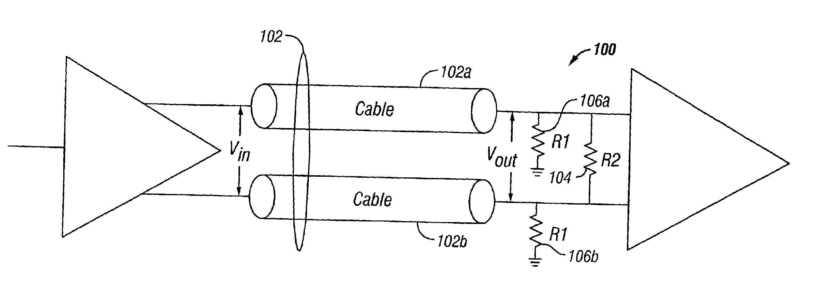
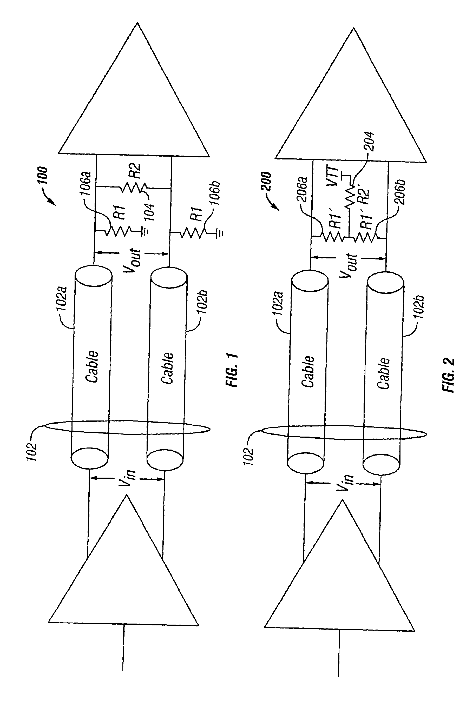
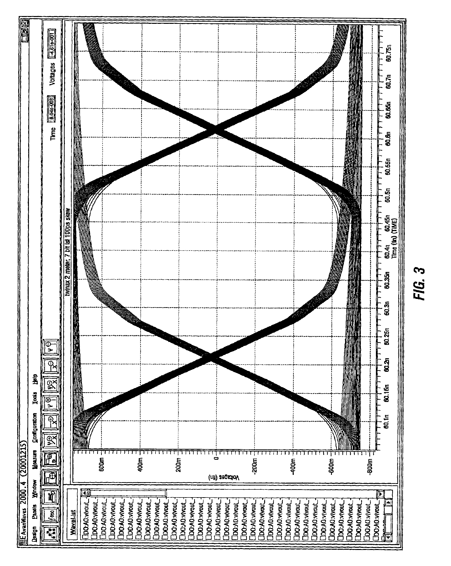
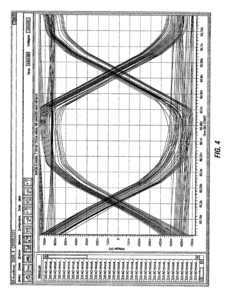
Improving signal integrity in differential signal systems
PatentInactiveUS6886065B2
Innovation
- Over-terminating the differential mode impedance of transmission lines, such as INFINIBAND cables, at the receiving end improves signal integrity by increasing eye-opening characteristics, using termination networks like pi-termination and T-termination networks to match both differential and common mode impedances effectively.
Power-Performance Tradeoffs in GDDR7 Design
The design of GDDR7 memory systems presents significant power-performance tradeoffs that must be carefully balanced to achieve optimal system operation. As signaling rates approach 40 Gbps and beyond, power consumption becomes a critical constraint that directly impacts thermal management, battery life in mobile applications, and overall system efficiency.
Power consumption in GDDR7 interfaces scales approximately quadratically with frequency, creating challenging design constraints. The increased power requirements for maintaining signal integrity at higher data rates necessitate sophisticated power management techniques. Designers must implement dynamic voltage and frequency scaling (DVFS) algorithms that can adaptively adjust operating parameters based on workload demands.
Equalization circuits, essential for maintaining adequate eye openings at high speeds, represent a significant portion of the power budget. Decision Feedback Equalization (DFE) and Feed-Forward Equalization (FFE) circuits consume substantial power but are necessary to counteract channel impairments. Advanced equalization techniques that optimize power efficiency while maintaining signal integrity are becoming critical differentiators in GDDR7 designs.
Termination schemes present another important tradeoff area. While proper termination is essential for signal integrity, each termination resistor consumes power proportional to the square of the voltage swing. Adaptive termination schemes that dynamically adjust based on operating conditions can provide significant power savings during periods of reduced activity.
Clock distribution networks in GDDR7 systems also contribute substantially to power consumption. Forwarded clock architectures, while beneficial for jitter performance, require careful power optimization. Implementing clock gating and frequency scaling during idle periods can significantly reduce average power consumption without compromising performance during active operation.
The voltage margins required for reliable operation directly impact power consumption. Tighter control of manufacturing processes and improved adaptive calibration techniques allow for reduced voltage margins while maintaining reliability. Every 100mV reduction in operating voltage can yield approximately 15-20% power savings in typical GDDR7 implementations.
Advanced packaging technologies, including silicon interposers and through-silicon vias (TSVs), offer opportunities to reduce trace lengths and improve signal integrity with lower power requirements. However, these technologies introduce additional manufacturing complexity and cost considerations that must be factored into overall system design decisions.
EMI Compliance and Certification Requirements
Electromagnetic Interference (EMI) compliance represents a critical consideration in the development and implementation of GDDR7 memory interfaces. As signal speeds approach 40 Gbps and beyond, the potential for electromagnetic emissions increases significantly, necessitating rigorous adherence to international standards and certification requirements. The Federal Communications Commission (FCC) in the United States, the European Union's CE marking requirements, and international standards such as CISPR 22/EN 55022 establish specific limits for radiated and conducted emissions that GDDR7 implementations must satisfy.
For GDDR7 memory interfaces, compliance testing typically involves measurements in both near-field and far-field environments, with particular attention to frequencies ranging from 30 MHz to 40 GHz. The high-speed differential signaling employed in GDDR7 interfaces creates potential radiation sources, especially at points where signal integrity is compromised due to impedance discontinuities or inadequate equalization.
Signal integrity challenges in GDDR7 directly impact EMI performance. Insufficient eye openings and excessive jitter can lead to increased electromagnetic emissions as signals transition through non-linear regions of operation. Consequently, the equalization techniques employed to maintain signal integrity also serve as primary EMI mitigation strategies. Advanced equalization methods such as Decision Feedback Equalization (DFE) and Continuous Time Linear Equalization (CTLE) must be optimized not only for data integrity but also for EMI compliance.
Board-level design considerations for EMI compliance include careful routing of differential pairs, strategic placement of ground planes, and implementation of guard traces. The stackup design must account for both signal integrity and EMI control, often requiring simulation-based optimization before physical implementation. Shielding techniques and filter components may be necessary at critical points in the signal path to attenuate unwanted emissions.
Pre-compliance testing has become essential in the development cycle for GDDR7 interfaces, allowing designers to identify and address potential EMI issues before formal certification testing. This typically involves near-field scanning to identify emission hotspots, followed by targeted modifications to layout, component selection, or equalization parameters.
Certification requirements vary by region and application domain, with more stringent standards applying to automotive and aerospace implementations compared to consumer electronics. Documentation requirements for certification include detailed test reports, technical construction files, and declarations of conformity that demonstrate the product's compliance with all applicable standards and regulations.
Unlock deeper insights with Patsnap Eureka Quick Research — get a full tech report to explore trends and direct your research. Try now!
Generate Your Research Report Instantly with AI Agent
Supercharge your innovation with Patsnap Eureka AI Agent Platform!