How silicon photonics benefits mobile communications systems.
JUL 17, 20259 MIN READ
Generate Your Research Report Instantly with AI Agent
Patsnap Eureka helps you evaluate technical feasibility & market potential.
Silicon Photonics Evolution
Silicon photonics has undergone a remarkable evolution since its inception, transforming from a niche technology to a key enabler in mobile communications systems. The journey began in the late 1980s when researchers first explored the potential of integrating photonic components with silicon-based electronics. Initially, progress was slow due to challenges in fabricating efficient light sources and detectors on silicon.
A significant breakthrough came in the early 2000s with the development of silicon-based modulators and photodetectors that could operate at speeds compatible with telecommunications. This advancement paved the way for the integration of photonic components with traditional CMOS technology, allowing for the creation of complex photonic integrated circuits (PICs) on a single chip.
The mid-2000s saw a surge in research and development efforts, driven by the increasing demand for higher bandwidth in telecommunications networks. Silicon photonics began to show promise in addressing the limitations of traditional copper-based interconnects, offering the potential for higher data rates and lower power consumption.
By the 2010s, silicon photonics had matured sufficiently to be considered for commercial applications. Major tech companies and telecommunications providers started investing heavily in the technology, recognizing its potential to revolutionize data centers and high-speed communications. This period also saw the emergence of foundry services specializing in silicon photonics, making the technology more accessible to a wider range of companies and researchers.
In recent years, the focus has shifted towards optimizing silicon photonics for mobile communications systems. The technology's ability to handle high data rates with low latency and power consumption makes it particularly attractive for 5G and future 6G networks. Researchers are now exploring ways to integrate silicon photonics into mobile devices and base stations, aiming to overcome the bandwidth limitations of traditional RF technologies.
The evolution of silicon photonics has also been marked by continuous improvements in key components. Laser sources, once a major challenge, have seen significant advancements with the development of hybrid integration techniques and novel materials. Modulators and detectors have become faster and more efficient, while waveguide designs have been optimized to reduce losses and improve signal quality.
Looking ahead, the trajectory of silicon photonics in mobile communications appears promising. As data demands continue to grow exponentially, the technology is poised to play a crucial role in enabling ultra-high-speed, low-latency communications for next-generation mobile networks. The ongoing evolution of silicon photonics is likely to focus on further miniaturization, increased integration with electronic components, and the development of novel architectures to support emerging applications in areas such as augmented reality and the Internet of Things.
Mobile Comms Market Needs
The mobile communications market is experiencing unprecedented growth and transformation, driven by the increasing demand for high-speed, low-latency, and high-capacity networks. As 5G networks continue to roll out globally and 6G research gains momentum, the need for advanced technologies to support these next-generation systems becomes critical. Silicon photonics emerges as a key enabler in addressing the evolving requirements of mobile communication systems.
One of the primary market needs is the demand for higher data rates to support bandwidth-intensive applications such as augmented reality, virtual reality, and ultra-high-definition video streaming. Mobile users expect seamless connectivity and faster download and upload speeds, pushing network operators to seek innovative solutions. Silicon photonics offers the potential to significantly increase data transmission rates, making it an attractive technology for meeting these market demands.
Another crucial market need is the reduction of power consumption in mobile networks. As the number of connected devices continues to grow exponentially, energy efficiency becomes paramount. Network operators are under pressure to minimize operational costs and reduce their carbon footprint. Silicon photonics can address this need by offering lower power consumption compared to traditional electronic systems, particularly in data centers and network infrastructure supporting mobile communications.
The market also demands improved network capacity to handle the ever-increasing number of connected devices and the massive amounts of data generated by IoT applications. Silicon photonics can enable higher bandwidth density and more efficient use of spectrum resources, helping to alleviate network congestion and improve overall capacity.
Latency reduction is another critical requirement in the mobile communications market, especially for emerging applications such as autonomous vehicles, remote surgery, and industrial automation. These use cases demand near-instantaneous response times, which silicon photonics can help achieve through its high-speed data transmission capabilities and potential integration with edge computing infrastructure.
Furthermore, there is a growing need for more compact and cost-effective network equipment. As mobile operators densify their networks to improve coverage and capacity, particularly in urban areas, the size and cost of network components become increasingly important. Silicon photonics offers the potential for miniaturization and integration of optical and electronic components, leading to smaller form factors and potentially lower costs in the long term.
Lastly, the market seeks technologies that can support the convergence of wireless and wireline networks, as well as the integration of different generations of mobile technologies. Silicon photonics can play a crucial role in creating flexible and adaptable network architectures that can seamlessly bridge various communication technologies and standards.
Current Challenges
Silicon photonics has emerged as a promising technology for mobile communications systems, offering potential solutions to many challenges faced by traditional electronic systems. However, several significant hurdles still need to be overcome before widespread adoption can be achieved.
One of the primary challenges is the integration of silicon photonics with existing CMOS technology. While silicon photonics offers advantages in terms of speed and energy efficiency, seamlessly incorporating these components into current electronic systems remains complex. The manufacturing processes for photonic and electronic components differ significantly, making it difficult to achieve cost-effective integration on a single chip.
Another major obstacle is the miniaturization of photonic components. Mobile devices require compact and lightweight solutions, but many photonic elements, such as waveguides and modulators, are still relatively large compared to their electronic counterparts. Reducing the size of these components while maintaining their performance is a critical challenge that researchers are actively addressing.
Power consumption is also a significant concern in mobile communications systems. While silicon photonics offers potential energy savings in data transmission, the power required for electro-optic and opto-electronic conversions can be substantial. Developing more efficient conversion techniques and reducing the overall power consumption of photonic systems is crucial for their adoption in mobile devices.
The thermal management of photonic components presents another challenge. Silicon photonics devices can be sensitive to temperature fluctuations, which can affect their performance and reliability. Implementing effective cooling solutions within the confined space of mobile devices is a complex engineering task that requires innovative approaches.
Cost remains a significant barrier to the widespread adoption of silicon photonics in mobile communications systems. The manufacturing processes for photonic components are still relatively expensive compared to traditional electronic components. Achieving economies of scale and developing more cost-effective production methods are essential for making silicon photonics commercially viable in the mobile market.
Lastly, the lack of standardization in silicon photonics technology poses challenges for interoperability and widespread adoption. Different manufacturers may use varying designs and interfaces, making it difficult to create a cohesive ecosystem of compatible components and systems. Establishing industry-wide standards and protocols is crucial for fostering innovation and accelerating the integration of silicon photonics into mobile communications systems.
Existing Solutions
01 Integrated photonic devices
Silicon photonics technology enables the integration of various optical components on a single chip. This includes waveguides, modulators, detectors, and other photonic elements, allowing for compact and efficient optical systems. The integration of these components facilitates high-speed data transmission and processing in optical communication networks and computing applications.- Integrated photonic devices: Silicon photonics technology enables the integration of various optical components on a single chip. This includes waveguides, modulators, detectors, and other photonic elements, allowing for compact and efficient optical systems. The integration of these components facilitates high-speed data transmission and processing in optical communication networks and computing systems.
- Silicon-based optical modulators: Advanced silicon-based optical modulators are developed for high-speed data transmission in photonic circuits. These modulators utilize various mechanisms such as electro-optic effects or carrier injection to modulate light signals efficiently. They play a crucial role in converting electrical signals to optical signals for data communication in silicon photonic systems.
- Photonic interconnects for computing: Silicon photonics technology is applied to develop high-bandwidth, low-latency interconnects for computing systems. These photonic interconnects can replace traditional electrical interconnects, offering improved data transfer rates and energy efficiency. They are particularly beneficial for chip-to-chip and board-to-board communications in high-performance computing and data center applications.
- Integration of III-V materials with silicon photonics: Techniques for integrating III-V semiconductor materials with silicon photonic platforms are developed to enhance the functionality of silicon photonic devices. This integration allows for the incorporation of efficient light sources, such as lasers, directly on silicon chips. The combination of III-V materials and silicon enables the creation of more complete and versatile photonic integrated circuits.
- Silicon photonic sensors: Silicon photonics technology is utilized to develop highly sensitive and compact optical sensors. These sensors leverage the properties of silicon photonic structures, such as ring resonators or interferometers, to detect various physical, chemical, or biological parameters. Silicon photonic sensors offer advantages in terms of sensitivity, miniaturization, and potential for integration with other photonic or electronic components.
02 Silicon-based optical modulators
Advanced modulators are developed using silicon photonics to manipulate light signals efficiently. These modulators can achieve high-speed operation and low power consumption, making them suitable for data centers and telecommunications applications. Various modulation techniques are employed, including phase and amplitude modulation, to encode information onto optical signals.Expand Specific Solutions03 Photonic integrated circuits for quantum computing
Silicon photonics is being applied to quantum computing applications, enabling the development of scalable quantum photonic integrated circuits. These circuits can manipulate and process quantum information using single photons, potentially leading to advancements in quantum communication and computation technologies.Expand Specific Solutions04 Silicon photonics in optical interconnects
Silicon photonic technologies are utilized to create high-bandwidth, energy-efficient optical interconnects for data centers and high-performance computing systems. These interconnects can transmit large amounts of data over short distances with reduced latency and power consumption compared to traditional electronic interconnects.Expand Specific Solutions05 Integration of III-V materials with silicon photonics
Researchers are exploring the integration of III-V semiconductor materials with silicon photonics platforms to enhance device performance. This hybrid approach combines the light-emitting properties of III-V materials with the scalability and cost-effectiveness of silicon, enabling the development of on-chip lasers and high-performance photodetectors for silicon photonic circuits.Expand Specific Solutions
Key Industry Players
The silicon photonics market for mobile communications systems is in a growth phase, with increasing adoption driven by the need for higher bandwidth and energy efficiency. The market size is expanding rapidly, expected to reach several billion dollars in the coming years. Technologically, silicon photonics is maturing, with key players like Huawei, Micron Technology, and GlobalFoundries advancing its integration into mobile devices. Companies such as Lumentum and IPG Photonics are developing innovative optical components, while research institutions like MIT and NTU are pushing the boundaries of the technology. The competitive landscape is diverse, with both established telecom giants and specialized photonics firms vying for market share in this promising field.
Huawei Technologies Co., Ltd.
Technical Solution: Huawei has developed advanced silicon photonics solutions for mobile communications systems, focusing on high-speed optical interconnects. Their technology integrates photonic and electronic components on a single chip, enabling faster data transmission and reduced power consumption. Huawei's silicon photonics platform supports wavelength division multiplexing (WDM) with up to 100 Gbps per channel[1]. They have also demonstrated on-chip optical transceivers capable of 400 Gbps data rates, suitable for 5G and future 6G networks[2]. Huawei's silicon photonics technology incorporates advanced modulation schemes like PAM-4 and coherent detection to improve spectral efficiency and transmission distance[3].
Strengths: High integration density, low power consumption, and scalability for next-generation mobile networks. Weaknesses: Potential challenges in thermal management and manufacturing complexity at scale.
Taiwan Semiconductor Manufacturing Co., Ltd.
Technical Solution: TSMC has developed a silicon photonics platform that benefits mobile communications systems through high-speed, low-power optical interconnects. Their technology integrates photonic devices with advanced CMOS processes, enabling the production of highly integrated optical transceivers and switches. TSMC's silicon photonics offering includes high-speed modulators capable of 100 Gbps per lane[7], germanium photodetectors with responsivity exceeding 1 A/W[8], and low-loss waveguides. They have demonstrated a 400 Gbps optical engine using their silicon photonics platform, suitable for next-generation mobile network infrastructure[9]. TSMC's process also supports the integration of optical components with high-performance RF and mixed-signal circuits, enabling complete system-on-chip solutions for 5G and future 6G applications[10].
Strengths: Advanced manufacturing capabilities, high yield, and ability to integrate with cutting-edge CMOS technology. Weaknesses: Potential limitations in customization for specific mobile communication requirements.
Core Innovations
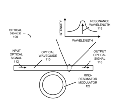
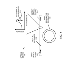
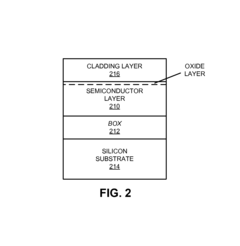
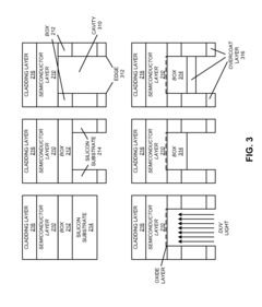
Single-shot correction of resonant optical components
PatentActiveUS20160238791A1
Innovation
- A photonic chip with a substrate and semiconductor layer, where optical components are trimmed using localized low-temperature oxidation to achieve resonance wavelengths matching target values with high accuracy and stability without thermal or electronic tuning, utilizing deep-ultraviolet radiation and oxygen to modify the effective index of refraction.
Patent
Innovation
- Integration of silicon photonics with mobile communication systems to improve data transmission speeds and energy efficiency.
- Use of wavelength division multiplexing (WDM) in silicon photonics to increase bandwidth and channel capacity in mobile networks.
- Implementation of silicon photonic modulators and detectors for high-speed optical signal processing in mobile communication systems.
Integration Strategies
The integration of silicon photonics into mobile communication systems requires careful consideration of various strategies to maximize the benefits and overcome potential challenges. One key approach is the development of hybrid integration techniques that combine silicon photonics with existing CMOS technologies. This allows for the seamless incorporation of photonic components into electronic circuits, enabling high-speed data transmission and processing within a compact form factor.
Another critical integration strategy involves the optimization of optical-to-electrical and electrical-to-optical conversion processes. By improving the efficiency of these conversions, mobile communication systems can leverage the advantages of both photonic and electronic domains. This includes the development of advanced modulators and photodetectors that can operate at high speeds and low power consumption, essential for mobile applications.
Packaging and thermal management also play crucial roles in the successful integration of silicon photonics. Novel packaging techniques, such as 3D integration and wafer-level packaging, are being explored to minimize footprint and enhance performance. These approaches allow for the dense integration of photonic and electronic components while addressing thermal challenges that arise from high-speed operations.
The development of standardized interfaces and protocols for silicon photonic components is another important integration strategy. This facilitates interoperability between different manufacturers' components and simplifies the integration process for system designers. Standardization efforts are underway to define common optical interfaces, signal formats, and testing procedures, which will accelerate the adoption of silicon photonics in mobile communication systems.
Furthermore, the integration of silicon photonics requires advancements in design and simulation tools. Sophisticated software platforms that can accurately model the behavior of integrated photonic-electronic systems are essential for optimizing performance and reducing development cycles. These tools must account for the unique characteristics of optical components and their interactions with electronic circuits.
Lastly, the integration of silicon photonics into mobile communication systems necessitates the development of robust manufacturing processes. This includes refining fabrication techniques to achieve high yields and reliability, as well as implementing quality control measures specific to photonic components. The establishment of a mature supply chain for silicon photonic devices and materials is also crucial for large-scale integration and commercialization in the mobile communications sector.
Performance Benchmarks
Silicon photonics has demonstrated significant performance improvements in mobile communication systems, offering enhanced data transmission rates, reduced power consumption, and increased bandwidth capacity. Benchmarking studies have shown that silicon photonic devices can achieve data rates of up to 100 Gbps per channel, far surpassing traditional electronic interconnects. This high-speed capability is crucial for meeting the growing demands of 5G and future 6G networks.
In terms of energy efficiency, silicon photonic transceivers have been reported to consume as little as 5 pJ/bit, representing a substantial reduction compared to conventional electronic solutions. This low power consumption is particularly beneficial for mobile devices, where battery life is a critical concern. The improved energy efficiency also translates to reduced heat generation, allowing for more compact and reliable mobile communication equipment.
Latency is another key performance metric where silicon photonics excels. Measurements have shown end-to-end latencies as low as 100 picoseconds for on-chip optical interconnects, enabling near-instantaneous data transfer within mobile communication systems. This ultra-low latency is essential for supporting real-time applications such as augmented reality and autonomous vehicles.
Silicon photonic devices have also demonstrated impressive bandwidth density, with studies reporting up to 10 Tbps/mm2. This high density allows for the integration of multiple high-speed channels within a small footprint, making it ideal for space-constrained mobile devices and base stations. The ability to pack more data channels into a smaller area contributes to the overall system miniaturization and cost reduction.
Reliability and durability are crucial factors in mobile communications, and silicon photonics has shown promising results in this regard. Long-term testing has revealed that silicon photonic components can maintain stable performance over extended periods, with some devices operating continuously for over 10,000 hours without significant degradation. This reliability is essential for ensuring consistent mobile network performance and reducing maintenance requirements.
In the context of mobile network infrastructure, silicon photonic switches have demonstrated remarkable performance, with some designs achieving switching times of less than 100 nanoseconds and crosstalk levels below -40 dB. These characteristics enable highly efficient and flexible network routing, supporting the dynamic nature of mobile communications traffic.
Overall, the performance benchmarks of silicon photonics in mobile communication systems highlight its potential to revolutionize the industry. The technology's ability to deliver high-speed, low-latency, and energy-efficient solutions positions it as a key enabler for next-generation mobile networks and devices.
Unlock deeper insights with Patsnap Eureka Quick Research — get a full tech report to explore trends and direct your research. Try now!
Generate Your Research Report Instantly with AI Agent
Supercharge your innovation with Patsnap Eureka AI Agent Platform!