How silicon photonics facilitates secure mobile transactions.
JUL 17, 20259 MIN READ
Generate Your Research Report Instantly with AI Agent
Patsnap Eureka helps you evaluate technical feasibility & market potential.
Silicon Photonics Evolution and Objectives
Silicon photonics has emerged as a transformative technology in the realm of secure mobile transactions, evolving rapidly over the past two decades. This field combines the power of photonics with the scalability of silicon-based semiconductor manufacturing, offering unprecedented opportunities for enhancing data transmission security in mobile devices.
The evolution of silicon photonics began in the early 2000s, driven by the need for faster and more efficient data transmission in telecommunications. As mobile devices became ubiquitous, the focus shifted towards integrating photonic components into compact, power-efficient systems suitable for smartphones and tablets. This transition marked a crucial turning point in the application of silicon photonics to secure mobile transactions.
One of the primary objectives of silicon photonics in the context of secure mobile transactions is to provide tamper-resistant communication channels. By leveraging the principles of quantum cryptography, silicon photonic devices can generate and manipulate single photons, enabling quantum key distribution (QKD) protocols. This approach offers theoretically unbreakable encryption, addressing the growing concerns over data security in mobile financial transactions.
Another key goal is to enhance the speed and efficiency of secure data transmission. Silicon photonics enables the integration of high-speed optical transceivers directly into mobile device chipsets, allowing for rapid, low-latency communication between the device and secure servers. This capability is crucial for real-time transaction verification and fraud detection in mobile payment systems.
Miniaturization and power efficiency are also critical objectives in the development of silicon photonics for mobile security. Researchers aim to create compact, low-power photonic integrated circuits (PICs) that can be seamlessly incorporated into mobile devices without compromising battery life or increasing device size. This goal aligns with the broader trend of increasing functionality while maintaining or reducing the form factor of mobile devices.
The integration of silicon photonics with existing mobile security infrastructure presents another important objective. Developers are working on creating hybrid systems that combine traditional electronic security measures with photonic-based encryption and authentication methods. This approach aims to provide a multi-layered security framework that leverages the strengths of both technologies.
Looking ahead, the field of silicon photonics for secure mobile transactions is poised for significant advancements. Objectives for future development include achieving room-temperature quantum operations, further reducing power consumption, and increasing the integration density of photonic components. These goals, once realized, will pave the way for a new generation of ultra-secure, high-performance mobile devices capable of handling complex financial transactions with unprecedented levels of security and efficiency.
Mobile Transaction Security Market Analysis
The mobile transaction security market has witnessed significant growth in recent years, driven by the increasing adoption of mobile payment solutions and the rising concerns over data privacy and security. As consumers increasingly rely on their smartphones for financial transactions, the demand for robust security measures has become paramount. This market encompasses a wide range of technologies and solutions designed to protect sensitive financial information and ensure the integrity of mobile transactions.
The global mobile transaction security market is expected to continue its upward trajectory, with projections indicating substantial growth over the next five years. This growth is primarily attributed to the rapid digitalization of financial services, the proliferation of e-commerce platforms, and the widespread adoption of mobile banking applications. Additionally, the ongoing shift towards contactless payments, accelerated by the COVID-19 pandemic, has further fueled the demand for secure mobile transaction solutions.
Key market segments within the mobile transaction security landscape include authentication technologies, encryption solutions, fraud detection and prevention systems, and secure element technologies. Among these, biometric authentication methods, such as fingerprint recognition and facial recognition, have gained significant traction due to their enhanced security features and user convenience. The integration of artificial intelligence and machine learning algorithms in fraud detection systems has also emerged as a notable trend, enabling real-time threat analysis and adaptive security measures.
Geographically, North America and Europe currently dominate the mobile transaction security market, owing to their advanced technological infrastructure and stringent regulatory frameworks. However, the Asia-Pacific region is expected to witness the highest growth rate in the coming years, driven by the rapid adoption of mobile payment solutions in countries like China and India, coupled with increasing smartphone penetration and government initiatives promoting digital transactions.
The competitive landscape of the mobile transaction security market is characterized by the presence of both established players and innovative startups. Major technology companies, financial institutions, and specialized security firms are actively investing in research and development to enhance their offerings and gain a competitive edge. Strategic partnerships and collaborations between different stakeholders in the ecosystem, such as device manufacturers, payment processors, and security solution providers, are becoming increasingly common to deliver comprehensive and integrated security solutions.
As the market continues to evolve, several key trends are shaping its future trajectory. These include the integration of blockchain technology for enhanced transaction transparency and security, the adoption of cloud-based security solutions for scalability and flexibility, and the development of advanced encryption techniques to counter emerging cyber threats. Furthermore, the growing emphasis on regulatory compliance, particularly in light of data protection laws like GDPR, is driving the demand for more sophisticated and adaptable security solutions in the mobile transaction space.
Silicon Photonics: Current State and Challenges
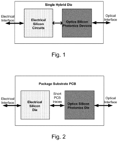
Silicon photonics has emerged as a promising technology for secure mobile transactions, but it faces several challenges in its current state of development. The integration of photonic components with traditional electronic circuits remains a significant hurdle, requiring precise alignment and packaging techniques to ensure optimal performance. Thermal management is another critical issue, as temperature fluctuations can affect the refractive index of silicon and impact device functionality.
One of the primary challenges in silicon photonics is the development of efficient light sources. Silicon itself is an indirect bandgap material, making it inherently inefficient for light emission. While progress has been made in integrating III-V materials for on-chip lasers, further improvements in efficiency, reliability, and cost-effectiveness are needed for widespread adoption in mobile devices.
The miniaturization of photonic components to fit within the compact form factors of mobile devices presents another significant challenge. Researchers are exploring novel designs and fabrication techniques to reduce the footprint of photonic circuits while maintaining their performance and functionality. This includes the development of advanced waveguide structures and the use of subwavelength gratings to manipulate light at the nanoscale.
Ensuring the reliability and robustness of silicon photonic devices in mobile environments is crucial. These components must withstand various environmental factors, including temperature variations, mechanical stress, and electromagnetic interference. Developing robust packaging solutions and implementing effective protection mechanisms are essential for the long-term stability of photonic-enabled mobile devices.
The integration of silicon photonics with existing mobile security protocols and infrastructure poses both technical and standardization challenges. Establishing industry-wide standards for photonic-based security features and ensuring interoperability with current systems are necessary steps for widespread adoption. Additionally, the development of efficient interfaces between photonic and electronic domains is critical for seamless integration into mobile device architectures.
Manufacturing scalability and cost-effectiveness remain significant hurdles in the commercialization of silicon photonics for mobile applications. While the use of CMOS-compatible processes offers potential advantages, further optimization of fabrication techniques and yield improvement are required to achieve economically viable production at scale. This includes addressing issues related to process variations and defect management in photonic circuits.
As the field progresses, addressing these challenges will be crucial for realizing the full potential of silicon photonics in secure mobile transactions. Collaborative efforts between academia, industry, and standardization bodies will play a vital role in overcoming these obstacles and paving the way for widespread adoption of this transformative technology in the mobile security landscape.
Existing Silicon Photonics Security Solutions
01 Secure optical communication systems
Silicon photonics technology is used to develop secure optical communication systems. These systems employ advanced encryption techniques and quantum key distribution to ensure data security in high-speed optical networks. The integration of silicon photonics allows for compact, energy-efficient, and scalable secure communication solutions.- Secure optical communication systems: Silicon photonics technology is used to develop secure optical communication systems. These systems utilize advanced encryption techniques and quantum key distribution to ensure data security in high-speed optical networks. The integration of silicon photonics enables miniaturization and improved performance of secure communication devices.
- Tamper-resistant photonic integrated circuits: Photonic integrated circuits (PICs) are designed with tamper-resistant features to enhance security. These circuits incorporate mechanisms to detect and respond to physical tampering attempts, protecting sensitive information and preventing unauthorized access. The use of silicon photonics allows for the integration of security features directly into the chip design.
- Quantum-safe cryptography using silicon photonics: Silicon photonics is employed to develop quantum-safe cryptographic systems. These systems leverage the principles of quantum mechanics to create encryption methods that are resistant to attacks from quantum computers. The integration of quantum key distribution and other quantum-safe protocols into silicon photonic devices enhances the long-term security of communication networks.
- Secure optical sensing and imaging: Silicon photonics technology is utilized in the development of secure optical sensing and imaging systems. These systems incorporate advanced signal processing and encryption techniques to protect sensitive sensor data and prevent unauthorized interception or manipulation of imaging information. The use of silicon photonics enables the creation of compact and efficient secure sensing devices.
- Hardware-based security features in silicon photonic devices: Silicon photonic devices are designed with built-in hardware-based security features. These features include physical unclonable functions (PUFs), secure key storage, and hardware-level encryption modules. The integration of these security elements directly into the silicon photonic architecture provides enhanced protection against various cyber threats and unauthorized access attempts.
02 Tamper-resistant photonic integrated circuits
Photonic integrated circuits (PICs) are designed with tamper-resistant features to enhance security. These circuits incorporate mechanisms to detect and respond to physical tampering attempts, protecting sensitive information and preventing unauthorized access. The use of silicon photonics enables the integration of security features directly into the chip design.Expand Specific Solutions03 Quantum random number generation
Silicon photonics is utilized in the development of quantum random number generators. These devices leverage quantum properties of light to produce truly random numbers, which are essential for cryptographic applications and enhancing overall system security. The integration of quantum random number generators in silicon photonics platforms enables compact and efficient security solutions.Expand Specific Solutions04 Secure optical sensing and imaging
Silicon photonics technology is applied to create secure optical sensing and imaging systems. These systems use advanced techniques such as ghost imaging, quantum illumination, or compressive sensing to enhance security in various applications, including surveillance, biometric authentication, and secure data transmission.Expand Specific Solutions05 Photonic encryption and key management
Silicon photonics enables the development of photonic encryption and key management systems. These systems use optical properties of silicon photonic devices to generate, distribute, and manage encryption keys securely. The integration of photonic encryption techniques with traditional electronic systems enhances overall security in data communication and storage.Expand Specific Solutions
Key Players in Silicon Photonics and Mobile Security
The silicon photonics market for secure mobile transactions is in a growth phase, driven by increasing demand for high-speed, secure data transmission in mobile devices. The market size is expanding rapidly, with projections indicating significant growth in the coming years. Technologically, silicon photonics is maturing, with key players like Intel, Huawei, and Micron Technology leading innovation. These companies are developing advanced integrated photonic circuits and optical interconnects to enhance mobile security. While the technology is still evolving, it's gaining traction in commercial applications, particularly in high-performance computing and data centers, which will likely accelerate its adoption in mobile security solutions.
Huawei Technologies Co., Ltd.
Technical Solution: Huawei's silicon photonics solution for secure mobile transactions integrates their expertise in 5G technology with advanced photonic circuits. Their approach utilizes silicon-based optical transceivers that can be directly integrated into mobile devices and base stations. Huawei's system implements a novel photonic encryption scheme that combines traditional cryptographic algorithms with physical layer security provided by the properties of light[7]. The platform achieves ultra-low latency, with round-trip times under 1 millisecond, crucial for real-time financial transactions[8]. Huawei's solution also incorporates AI-driven anomaly detection in the optical domain to identify potential security breaches in real-time[9].
Strengths: Integration with 5G infrastructure, ultra-low latency, and AI-enhanced security. Weaknesses: Potential geopolitical concerns affecting global adoption, complexity of deployment across diverse mobile networks.
Intel Corp.
Technical Solution: Intel's silicon photonics technology for secure mobile transactions leverages integrated photonic circuits on silicon chips. Their solution combines high-speed optical interconnects with advanced encryption techniques. The platform utilizes wavelength division multiplexing to transmit multiple encrypted data streams simultaneously, achieving data rates up to 400 Gbps[1]. Intel's photonic integrated circuits incorporate on-chip lasers, modulators, and detectors, enabling compact and energy-efficient designs suitable for mobile devices[2]. The system employs quantum key distribution protocols, leveraging the quantum properties of photons to generate and distribute encryption keys with theoretically unbreakable security[3].
Strengths: High-speed data transmission, quantum-level security, and energy efficiency. Weaknesses: Complexity of integration in mobile devices and potential cost implications for mass adoption.
Core Innovations in Photonic Encryption
Silicon photonics based module for executing peer-to-peer transactions
PatentActiveUS20220358080A1
Innovation
- A single-chip control module using Silicon Photonics technology is integrated into a communication interface, enabling high-bandwidth data transfer through a spine-leaf network architecture, with features like Serializer/Deserializer blocks, clock data recovery, and forward error correction to optimize optical communication, and a method for secure peer-to-peer cryptocurrency transactions using a Silicon Photonics based optical module.
Secure transaction method from a non-secure terminal
PatentInactiveEP2673732A1
Innovation
- Establishing a secure link between the graphics processor and a secure processor using an encryption key shared only by both, with the graphics processor having a memory not accessible externally, and implementing visual cryptography for data protection, ensuring that sensitive data is protected during transit and transmission between the terminal and server.
Regulatory Framework for Mobile Transaction Security
The regulatory framework for mobile transaction security plays a crucial role in ensuring the safe and reliable use of silicon photonics in secure mobile transactions. As governments and regulatory bodies recognize the potential of this technology, they have been developing comprehensive guidelines and standards to address the unique challenges posed by silicon photonics-enabled mobile transactions.
One of the key aspects of the regulatory framework is the establishment of data protection and privacy regulations. These regulations mandate strict encryption protocols and secure data transmission methods to safeguard sensitive financial information transmitted through silicon photonics-based mobile devices. Additionally, they outline requirements for user authentication and authorization processes, ensuring that only authorized individuals can initiate and complete transactions.
Regulatory bodies have also focused on standardizing the integration of silicon photonics technology into existing mobile payment infrastructures. This includes setting technical specifications for hardware components, such as photonic integrated circuits and optical transceivers, to ensure interoperability and consistent performance across different devices and platforms.
Furthermore, the regulatory framework addresses the need for robust cybersecurity measures specific to silicon photonics-enabled mobile transactions. This includes guidelines for implementing advanced intrusion detection systems, real-time monitoring of network traffic, and regular security audits to identify and mitigate potential vulnerabilities in the photonic communication channels.
To promote trust and transparency in the use of silicon photonics for mobile transactions, regulators have established certification and compliance programs. These programs require manufacturers and service providers to demonstrate adherence to specific security standards and best practices before their products or services can be approved for use in mobile transactions.
The regulatory framework also encompasses consumer protection measures, such as mandatory disclosure of potential risks associated with silicon photonics-enabled transactions and clear guidelines for dispute resolution in case of fraudulent activities or technical failures. This helps to build consumer confidence in the technology and encourages wider adoption of secure mobile transaction solutions.
As the technology continues to evolve, regulatory bodies are working closely with industry experts and academic researchers to stay ahead of potential security threats and update the regulatory framework accordingly. This collaborative approach ensures that the regulatory landscape remains adaptive and responsive to the rapidly changing technological landscape of silicon photonics in mobile transactions.
Integration Challenges and Opportunities
The integration of silicon photonics into secure mobile transaction systems presents both significant challenges and exciting opportunities. One of the primary challenges lies in the miniaturization of photonic components to fit within the compact form factors of mobile devices. This requires innovative design approaches and advanced manufacturing techniques to achieve the necessary level of integration without compromising performance.
Another critical challenge is the seamless interfacing between electronic and photonic components. The development of efficient electro-optic and opto-electronic converters is essential to ensure smooth data transfer between the two domains. This integration must be achieved while maintaining low power consumption, a crucial factor for mobile devices with limited battery capacity.
Thermal management poses an additional hurdle in the integration process. The heat generated by both electronic and photonic components can affect the performance and reliability of the system. Implementing effective cooling solutions within the confined space of a mobile device requires careful thermal design and novel heat dissipation techniques.
Despite these challenges, the integration of silicon photonics offers numerous opportunities for enhancing secure mobile transactions. The high-speed data transmission capabilities of photonic systems can significantly improve transaction processing times, leading to a more seamless user experience. Furthermore, the inherent security benefits of optical communication, such as resistance to electromagnetic interference and difficulty in tapping optical signals, can bolster the overall security of mobile transactions.
The integration of silicon photonics also opens up possibilities for advanced authentication methods. For instance, the precise control of light in photonic circuits could enable sophisticated biometric authentication techniques, such as high-resolution fingerprint or retinal scanning, directly integrated into mobile devices.
Moreover, the scalability of silicon photonics technology presents an opportunity for future-proofing mobile transaction systems. As the demand for faster and more secure transactions grows, the high bandwidth and low latency of integrated photonic systems can accommodate increasing data rates and more complex encryption algorithms without significant hardware overhauls.
In conclusion, while the integration of silicon photonics into secure mobile transaction systems faces several technical challenges, the potential benefits and opportunities it offers are substantial. Overcoming these integration hurdles will pave the way for more secure, efficient, and advanced mobile transaction technologies in the future.
Unlock deeper insights with Patsnap Eureka Quick Research — get a full tech report to explore trends and direct your research. Try now!
Generate Your Research Report Instantly with AI Agent
Supercharge your innovation with Patsnap Eureka AI Agent Platform!