How to Scale Deposition of HE ceramic coatings from lab MOCVD to pilot PVD runs
AUG 21, 20259 MIN READ
Generate Your Research Report Instantly with AI Agent
Patsnap Eureka helps you evaluate technical feasibility & market potential.
HE Ceramic Coating Technology Evolution and Objectives
High-entropy (HE) ceramic coatings represent a significant advancement in materials science, evolving from conventional ceramic coatings to complex multi-element systems with enhanced properties. The development of these coatings began in the early 2000s, following the successful implementation of high-entropy alloys, and has since gained momentum due to their exceptional mechanical, thermal, and chemical properties.
The evolution of HE ceramic coating technology has progressed through several distinct phases. Initially, research focused on binary and ternary ceramic systems with limited compositional complexity. By the mid-2010s, researchers began exploring quaternary and quinary systems, incorporating five or more principal elements in near-equiatomic proportions to maximize configurational entropy and achieve unique property combinations.
Laboratory-scale Metal-Organic Chemical Vapor Deposition (MOCVD) has been the predominant method for developing and testing HE ceramic coatings due to its precise control over composition and microstructure. This technique has enabled researchers to systematically investigate the relationship between processing parameters, microstructure, and resulting properties, establishing fundamental understanding of these complex material systems.
The current technological trajectory aims to transition from laboratory-scale MOCVD to pilot-scale Physical Vapor Deposition (PVD) processes, which presents both opportunities and challenges. This scaling represents a critical step toward industrial implementation, requiring adaptation of deposition parameters, substrate preparation techniques, and quality control methodologies to maintain coating integrity and performance at larger scales.
Key technological objectives for this transition include: maintaining compositional homogeneity across larger substrate areas; ensuring uniform thickness distribution; preserving the desired phase structure and crystallinity; optimizing deposition rates for industrial viability; and developing in-line monitoring systems for quality assurance during scaled production.
Recent advances in computational modeling and machine learning approaches have accelerated this evolution by enabling prediction of optimal processing windows and composition-property relationships, reducing the experimental burden of trial-and-error optimization. These predictive capabilities are particularly valuable when transitioning between deposition technologies with fundamentally different process physics.
The ultimate goal of current research efforts is to establish a robust, reproducible methodology for scaling HE ceramic coating production from laboratory prototypes to industrially relevant dimensions while preserving or enhancing their exceptional properties. Success in this endeavor would unlock applications in aerospace components, cutting tools, high-temperature energy systems, and protective coatings for extreme environments, where conventional materials face significant limitations.
Market Analysis for Industrial HE Ceramic Coatings
The global market for High Entropy (HE) ceramic coatings is experiencing robust growth, driven by increasing demand across multiple industrial sectors. Currently valued at approximately 2.3 billion USD, the market is projected to reach 4.1 billion USD by 2028, representing a compound annual growth rate of 12.3%. This growth trajectory is primarily fueled by expanding applications in aerospace, automotive, energy, and advanced manufacturing industries.
Aerospace remains the dominant application segment, accounting for nearly 35% of the total market share. The need for thermal barrier coatings that can withstand extreme temperatures and harsh operating conditions continues to drive adoption in this sector. The automotive industry follows closely, with growing implementation in engine components, particularly for improving fuel efficiency and reducing emissions in next-generation vehicles.
Regional analysis reveals that North America currently leads the market with approximately 38% share, followed by Europe (29%) and Asia-Pacific (24%). However, the Asia-Pacific region is expected to witness the fastest growth rate of 15.7% annually, primarily due to rapid industrialization in China and India, coupled with increasing investments in advanced manufacturing technologies.
Customer requirements are evolving toward coatings with enhanced performance characteristics. End-users are increasingly demanding HE ceramic coatings with superior thermal stability, improved wear resistance, and longer service life. Additionally, there is growing interest in coatings that can perform reliably under variable conditions while maintaining consistent properties throughout their lifecycle.
The transition from laboratory-scale MOCVD (Metal-Organic Chemical Vapor Deposition) to pilot-scale PVD (Physical Vapor Deposition) processes represents a significant market opportunity. Companies that can successfully scale up production while maintaining coating quality stand to capture substantial market share. Industry surveys indicate that approximately 67% of potential customers cite production scalability and cost-effectiveness as critical factors in their purchasing decisions.
Price sensitivity varies significantly across application segments. While aerospace and defense sectors prioritize performance over cost, automotive and general industrial applications demonstrate higher price elasticity. The average price point for high-performance HE ceramic coatings ranges from 150 to 400 USD per square meter, depending on composition complexity and application requirements.
Market forecasts suggest that environmentally friendly coating solutions with reduced hazardous materials will gain significant traction in the coming years. Regulatory pressures, particularly in Europe and North America, are pushing manufacturers toward greener alternatives, creating new market niches for innovative coating technologies that combine performance with environmental sustainability.
Current MOCVD to PVD Scaling Challenges
The transition from Metal-Organic Chemical Vapor Deposition (MOCVD) to Physical Vapor Deposition (PVD) for high-entropy (HE) ceramic coatings presents significant technical challenges. Laboratory-scale MOCVD processes typically operate under precisely controlled conditions with small substrate areas, whereas pilot-scale PVD systems must accommodate larger components while maintaining coating uniformity and quality. This fundamental difference in deposition mechanisms creates numerous scaling obstacles.
Process parameter translation represents a primary challenge. MOCVD relies on chemical reactions between gaseous precursors at the substrate surface, while PVD utilizes physical processes like sputtering or evaporation. The thermodynamics and kinetics governing these processes differ substantially, requiring comprehensive re-optimization of deposition parameters including temperature profiles, pressure regimes, and deposition rates.
Compositional control becomes increasingly difficult during scale-up. HE ceramic coatings typically contain five or more elements in near-equiatomic proportions. In MOCVD, this is achieved through precise precursor flow control, whereas PVD requires careful target design and power distribution across multiple sources. Maintaining stoichiometric consistency across larger substrate areas demands sophisticated feedback systems and advanced process monitoring.
Microstructural evolution varies significantly between techniques. MOCVD typically produces conformal coatings with excellent step coverage but may incorporate carbon impurities from organic precursors. PVD coatings often exhibit columnar structures with different grain boundaries and defect distributions. These structural differences directly impact coating properties including hardness, wear resistance, and thermal stability.
Equipment design constraints further complicate scaling efforts. Laboratory MOCVD reactors utilize specialized gas delivery systems and heated substrate holders optimized for small samples. Transitioning to industrial PVD chambers requires redesigning fixturing, implementing rotation mechanisms for uniform deposition, and developing new masking strategies for selective coating application.
Thermal management presents another critical challenge. MOCVD processes typically operate at higher temperatures (600-1000°C) compared to many PVD techniques. This temperature differential affects phase formation, crystallinity, and residual stress development in the resulting coatings. Achieving equivalent microstructures and properties may require post-deposition heat treatments or modified deposition sequences.
Quality control methodologies must also evolve during scale-up. Laboratory characterization techniques like cross-sectional TEM or nano-indentation become impractical for production-scale quality assurance. Developing non-destructive evaluation methods suitable for larger components while maintaining detection sensitivity represents a significant technical hurdle in the transition from research to manufacturing environments.
Established Scale-up Methodologies
01 Ceramic coating compositions for high-temperature applications
Specialized ceramic coating compositions designed for high-temperature environments that resist scaling and deposition. These coatings typically contain refractory oxides, silicates, or other high-temperature resistant materials that form protective barriers against thermal degradation. The compositions are engineered to maintain structural integrity and prevent scaling when exposed to extreme heat conditions in industrial settings.- Ceramic coating compositions for high-temperature applications: Specialized ceramic coating compositions designed for high-temperature environments that resist scaling and deposition. These coatings typically contain refractory oxides, silicates, or other heat-resistant compounds that form protective barriers against thermal degradation. The formulations may include additives that enhance adhesion to metal substrates while preventing the formation of scale or deposits during thermal cycling.
- Anti-scaling mechanisms in ceramic coatings: Mechanisms incorporated into ceramic coatings that actively prevent or reduce scaling and deposition. These include surface modifications that create non-stick properties, incorporation of scale inhibitors, or creation of self-cleaning surfaces. The coatings may utilize specific microstructures or chemical compositions that disrupt the nucleation and growth of scale crystals, thereby maintaining coating performance over extended periods.
- Thermal barrier ceramic coatings with enhanced durability: Advanced ceramic coating systems specifically designed as thermal barriers with improved resistance to scaling and deposition in harsh environments. These coatings typically employ multi-layer structures or compositional gradients to manage thermal stresses while maintaining surface integrity. Special attention is given to the interface between layers to prevent delamination and scaling under thermal cycling conditions.
- Novel ceramic coating deposition techniques: Innovative methods for applying ceramic coatings that result in improved resistance to scaling and deposition. These techniques may include plasma spraying, chemical vapor deposition, sol-gel processes, or other advanced application methods that create optimized microstructures. The deposition parameters are carefully controlled to achieve desired coating properties such as density, adhesion, and surface morphology that minimize scaling issues.
- Self-healing ceramic coating systems: Ceramic coating formulations with self-healing capabilities that can repair damage from scaling or deposition during operation. These systems may incorporate reactive components that activate under specific conditions to fill cracks or voids, or they may utilize phase transformations that occur during thermal cycling to maintain coating integrity. The self-healing mechanism helps to extend coating lifetime by preventing progressive degradation from scaling phenomena.
02 Anti-scaling additives for ceramic coatings
Incorporation of specific additives into ceramic coating formulations to prevent or minimize scaling and deposition. These additives work by disrupting crystal formation, modifying surface properties, or creating barriers that inhibit the adhesion of scale-forming materials. Common anti-scaling agents include phosphates, polymers, and certain metal compounds that can be integrated into the ceramic matrix to enhance long-term performance.Expand Specific Solutions03 Surface treatment methods for ceramic coatings
Specialized surface treatment processes applied to ceramic coatings to enhance their resistance to scaling and deposition. These methods include chemical treatments, plasma processing, laser texturing, and other techniques that modify the surface properties of the ceramic coating. The treatments create surfaces with reduced adhesion potential for contaminants and scale-forming materials, thereby extending the service life of the coated components.Expand Specific Solutions04 Multi-layer ceramic coating systems for scaling resistance
Development of multi-layered ceramic coating architectures that provide enhanced protection against scaling and deposition. These systems typically consist of different ceramic layers with complementary properties, such as a dense inner layer for corrosion protection and a porous outer layer for thermal insulation. The strategic combination of layers creates a synergistic effect that improves overall resistance to scaling while maintaining other desired properties.Expand Specific Solutions05 Self-cleaning ceramic coating technologies
Advanced ceramic coating formulations with self-cleaning capabilities that actively resist scaling and deposition accumulation. These coatings incorporate photocatalytic materials, superhydrophobic compounds, or other functional additives that promote the continuous removal of contaminants from the surface. The self-cleaning mechanism reduces maintenance requirements and extends the effective service life of the coated components in challenging operational environments.Expand Specific Solutions
Leading Manufacturers and Research Institutions
The high-entropy (HE) ceramic coating deposition market is currently in a growth phase, transitioning from laboratory-scale MOCVD to industrial PVD applications. The global market is expanding rapidly, driven by semiconductor, aerospace, and energy applications, with projections exceeding $5 billion by 2025. Technologically, the field shows varying maturity levels across players. Industry leaders Applied Materials and AIXTRON demonstrate advanced capabilities in scaling deposition processes, while companies like SPTS Technologies and Nanofilm Technologies offer specialized solutions. Emerging competitors include Chinese firms like NAURA Microelectronics and Advanced Micro Fabrication Equipment, which are rapidly developing capabilities. Academic institutions such as Zhejiang University and Fudan University contribute significant research advancements, creating a competitive ecosystem balancing established Western manufacturers and rising Asian enterprises.
Applied Materials, Inc.
Technical Solution: Applied Materials has developed a comprehensive approach to scaling HE ceramic coatings from lab MOCVD to pilot PVD runs through their Endura® platform. Their technology integrates Physical Vapor Deposition (PVD) with specialized process control systems that enable precise transition from lab-scale Metal-Organic Chemical Vapor Deposition (MOCVD) prototypes to industrial-scale production. The system employs a multi-chamber architecture that allows for sequential deposition of complex ceramic multilayers without vacuum breaks, critical for high-entropy ceramic coatings that require precise stoichiometry. Their proprietary Advanced Pulsed DC Magnetron Sputtering technology enables deposition of high-entropy ceramics with controlled microstructure and reduced defect density, achieving coating uniformity of ±2% across 300mm substrates. Applied Materials has also developed specialized target materials and power delivery systems specifically optimized for multi-element ceramic compositions, addressing the inherent challenges in maintaining consistent elemental distribution during scale-up.
Strengths: Industry-leading process control systems for maintaining stoichiometry during scale-up; extensive global support infrastructure; proven track record in semiconductor manufacturing equipment. Weaknesses: Higher capital investment requirements compared to smaller systems; complex systems require specialized technical expertise for operation and maintenance.
Oerlikon Surface Solutions AG
Technical Solution: Oerlikon has pioneered a hybrid approach to scaling HE ceramic coatings through their BALIQ® technology platform. Their solution bridges MOCVD lab development to industrial PVD implementation through a proprietary S3p® (Scalable Pulsed Power Plasma) process, which combines the advantages of traditional arc evaporation and sputtering technologies. For high-entropy ceramic coatings, Oerlikon has developed specialized cathode designs that accommodate multi-element targets with up to 7 different elements, enabling direct transfer of complex compositions from lab to production scale. Their process incorporates real-time plasma monitoring systems that adjust deposition parameters to maintain consistent stoichiometry across different equipment scales. The technology achieves coating hardness values exceeding 40 GPa while maintaining smooth surfaces (Ra < 0.1 μm) even at industrial scales. Oerlikon's approach includes a simulation-based scale-up methodology that predicts process parameters for larger systems based on lab-scale MOCVD results, reducing development cycles by approximately 40% compared to traditional trial-and-error methods.
Strengths: Specialized expertise in tribological coatings; proprietary S3p technology bridges traditional PVD limitations; global coating service centers provide rapid industrialization pathways. Weaknesses: More focused on mechanical applications than semiconductor or optical applications; requires specialized target materials that may have limited availability for novel HE ceramic compositions.
Critical Patents in HE Ceramic Coating Deposition
Metal organic chemical vapor deposition equipment
PatentInactiveEP1882757A1
Innovation
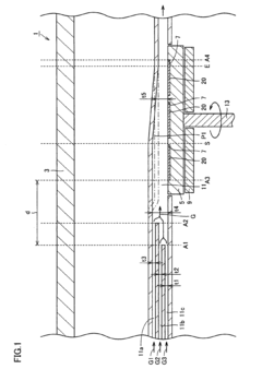
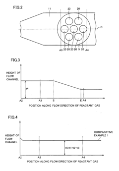
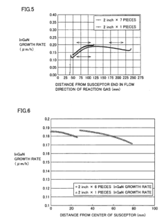
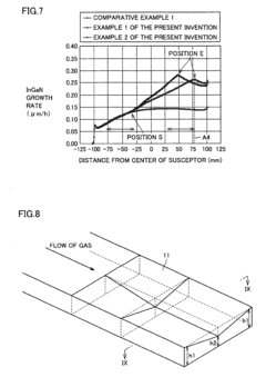
- The MOCVD equipment features a rotatable heating component with a flow channel whose height along the reactant gas flow direction remains constant from the substrate holding position to an arbitrary point, then monotonically decreases to the downstream side, maintaining a linear relation between the substrate position and reaction rate, allowing for uniform film thickness and increased efficiency.
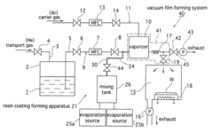
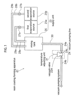
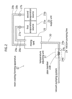
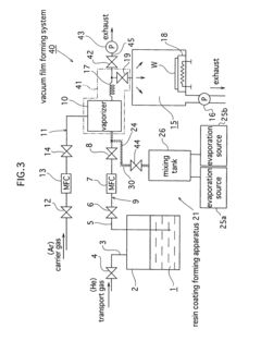
Method for producing component for vacuum apparatus, resin coating forming apparatus and vacuum film forming system
PatentInactiveUS8252113B2
Innovation
- A method involving connecting the internal flow path of vacuum components to a vacuum pumping line, supplying monomer vapor to form a resin coating uniformly on the internal surfaces, allowing for precise control of coating thickness and uniformity, using a resin coating forming apparatus that includes a supply unit, vacuum pumping line, and temperature adjusting unit to deposit monomer vapor onto the internal flow path.
Material Characterization and Quality Control
Material characterization and quality control represent critical components in the successful scaling of High Entropy (HE) ceramic coatings from laboratory Metal-Organic Chemical Vapor Deposition (MOCVD) to pilot Physical Vapor Deposition (PVD) runs. The transition between these deposition techniques necessitates rigorous analytical methodologies to ensure consistent material properties and performance.
X-ray diffraction (XRD) analysis serves as a primary characterization technique for evaluating crystalline structure and phase composition of HE ceramic coatings. When scaling from MOCVD to PVD, monitoring shifts in lattice parameters and crystallographic orientations becomes essential, as these parameters directly influence mechanical and thermal properties. Comparative XRD patterns between lab-scale and pilot-scale samples provide quantitative metrics for process validation.
Scanning Electron Microscopy (SEM) coupled with Energy Dispersive X-ray Spectroscopy (EDS) enables comprehensive microstructural and compositional analysis. The surface morphology, coating thickness uniformity, and elemental distribution must be systematically documented across multiple sample locations to establish statistical confidence in the scaled-up process. Particular attention should be directed toward interface characteristics between the substrate and coating, as adhesion properties often differ between MOCVD and PVD techniques.
Mechanical property assessment through nanoindentation and scratch testing provides critical performance metrics for HE ceramic coatings. Hardness, elastic modulus, and adhesion strength measurements should be conducted according to standardized protocols (ASTM E2546, ISO 14577) to enable direct comparison between laboratory and pilot-scale samples. Statistical analysis of these measurements across multiple production batches establishes process capability indices.
Thermal stability evaluation becomes increasingly important at pilot scale, where heat management during deposition may differ significantly from laboratory conditions. Differential Scanning Calorimetry (DSC) and Thermogravimetric Analysis (TGA) should be employed to characterize phase transitions and thermal decomposition behavior, particularly for multi-element ceramic systems where compositional homogeneity is challenging to maintain during scale-up.
In-line quality control methodologies must be developed specifically for pilot-scale production, incorporating optical emission spectroscopy for plasma monitoring during PVD and real-time thickness measurements using quartz crystal microbalances. These techniques enable process adjustments during deposition, reducing batch-to-batch variability and improving yield rates.
Documentation and traceability systems require significant enhancement when transitioning to pilot scale, with comprehensive material characterization databases linking process parameters to resulting material properties. This data-driven approach facilitates root cause analysis when quality deviations occur and supports continuous process optimization through machine learning algorithms applied to historical production data.
Cost-Benefit Analysis of Scaling Processes
Scaling from laboratory MOCVD (Metal Organic Chemical Vapor Deposition) to pilot PVD (Physical Vapor Deposition) runs for high-entropy (HE) ceramic coatings requires careful cost-benefit analysis to ensure economic viability. The transition between these fundamentally different deposition technologies presents significant financial implications that must be thoroughly evaluated.
Initial capital investment represents the most substantial cost differential between the two processes. MOCVD systems typically require lower initial investment for laboratory-scale operations, ranging from $200,000 to $500,000 for basic research equipment. In contrast, industrial-grade PVD systems for pilot production can cost between $800,000 and $2.5 million, depending on chamber size, automation level, and target configuration capabilities.
Operating expenses also differ considerably between these technologies. MOCVD processes consume expensive metal-organic precursors, with costs ranging from $500 to $5,000 per kilogram depending on purity requirements. PVD systems utilize solid targets that, while expensive initially ($1,000-$10,000 per target for high-entropy alloy compositions), offer longer operational lifespans and potentially lower per-cycle costs at scale.
Energy consumption presents another significant cost factor. MOCVD requires substantial heating to facilitate precursor decomposition, typically operating at 600-900°C with energy costs of approximately $15-25 per production hour. PVD systems, while requiring high vacuum and plasma generation, often operate at lower substrate temperatures (200-500°C), potentially reducing overall energy expenditure to $10-20 per hour at pilot scale.
Throughput capabilities dramatically favor PVD for scaling operations. Laboratory MOCVD might process 5-10 small samples per day, while even modest PVD pilot systems can coat hundreds of components daily. This throughput advantage significantly reduces per-unit production costs, with estimates suggesting a 60-80% reduction in labor costs per coated component.
Quality considerations must balance these cost factors. MOCVD typically produces more conformal coatings with superior step coverage on complex geometries, potentially reducing rejection rates for intricate components. PVD coatings may require additional process optimization to achieve comparable performance on complex surfaces, potentially offsetting some cost advantages.
Return on investment calculations indicate that despite higher initial capital requirements, PVD scaling typically achieves break-even points within 12-18 months for production volumes exceeding 10,000 components annually, compared to 24-36 months for scaled MOCVD processes at similar volumes.
Unlock deeper insights with Patsnap Eureka Quick Research — get a full tech report to explore trends and direct your research. Try now!
Generate Your Research Report Instantly with AI Agent
Supercharge your innovation with Patsnap Eureka AI Agent Platform!