

Multi-Bit Storage Techniques In Analog In-Memory Computing Arrays
SEP 2, 20259 MIN READ
Generate Your Research Report Instantly with AI Agent
PatSnap Eureka helps you evaluate technical feasibility & market potential.
Multi-Bit Storage Evolution and Objectives
Analog in-memory computing (AIMC) arrays have evolved significantly over the past decades, transitioning from simple single-bit storage to sophisticated multi-bit capabilities. The journey began in the 1970s with the introduction of floating-gate transistors for non-volatile memory applications, which laid the groundwork for multi-level cell (MLC) technologies. By the 1990s, flash memory had incorporated 2-bit storage per cell, marking the first commercial implementation of multi-bit storage.
The evolution accelerated in the 2000s with the emergence of resistive random-access memory (RRAM), phase-change memory (PCM), and magnetic random-access memory (MRAM) technologies. These novel memory architectures offered inherent analog characteristics suitable for multi-bit storage, with PCM demonstrating up to 4 bits per cell by 2010 through precise resistance level control.
The convergence with neuromorphic computing around 2015 represented a pivotal moment, as researchers recognized that the analog nature of emerging memory devices aligned perfectly with the computational needs of neural networks. This synergy catalyzed research into multi-bit storage specifically optimized for in-memory computing applications, where memory elements not only store information but also perform computations.
Recent advancements have focused on improving the precision, reliability, and energy efficiency of multi-bit storage in AIMC arrays. Techniques such as adaptive programming algorithms, temperature compensation, and drift mitigation have been developed to address the inherent variability and non-idealities of analog devices. The state-of-the-art now demonstrates 8-bit effective precision in some experimental platforms, though commercial implementations typically remain at 4-6 bits per cell.
The primary objectives for multi-bit storage in AIMC arrays center around several key dimensions. First, increasing storage density to maximize the computational capacity per unit area, with targets exceeding 8 bits per cell while maintaining acceptable error rates. Second, improving programming accuracy to ensure reliable representation of weights in neural network applications. Third, enhancing retention characteristics to maintain multi-bit precision over extended periods without refresh operations.
Energy efficiency represents another critical objective, with research aiming to reduce programming energy while maintaining precision. Speed optimization focuses on decreasing the latency of multi-bit programming operations, particularly for applications requiring frequent weight updates. Finally, scalability objectives address the challenges of maintaining multi-bit precision as array sizes increase to accommodate larger neural network models, with particular emphasis on mitigating line resistance effects and device-to-device variability.
Market Analysis for Analog In-Memory Computing
The analog in-memory computing (AIMC) market is experiencing significant growth driven by the increasing demand for energy-efficient AI hardware solutions. Current market projections indicate that the broader AI hardware market, which includes AIMC technologies, will reach approximately $115 billion by 2025, with a compound annual growth rate exceeding 20%. Within this broader market, analog computing solutions are expected to capture an increasing share as organizations seek alternatives to traditional von Neumann architectures.
The primary market drivers for AIMC technologies include the exponential growth in AI workloads, escalating data center energy costs, and the expanding edge computing ecosystem. Data centers currently consume over 1% of global electricity, with AI training and inference representing a rapidly growing portion of this consumption. This creates a compelling economic case for AIMC solutions, which can potentially reduce energy consumption by 10-100x compared to digital alternatives for certain workloads.
Multi-bit storage techniques in AIMC arrays are particularly valuable in this market context, as they directly address the density-accuracy tradeoff that has limited commercial adoption. The ability to store multiple bits per memory cell can increase computational density while maintaining acceptable accuracy levels for production AI systems. This capability is especially relevant for edge applications where device footprint and power constraints are significant limiting factors.
Market segmentation reveals three primary customer categories for multi-bit AIMC technologies: cloud service providers seeking data center efficiency improvements, edge device manufacturers requiring low-power AI capabilities, and specialized high-performance computing users in sectors such as scientific research, finance, and autonomous systems. Each segment values different aspects of the technology, from energy efficiency to computational density to inference speed.
Regional market analysis shows North America leading in AIMC research and investment, with approximately 45% of related patents and venture funding. Asia-Pacific represents the fastest-growing market, particularly in China, South Korea, and Taiwan, where semiconductor manufacturing expertise aligns well with AIMC hardware requirements. Europe maintains a strong position in research but lags in commercialization efforts.
The total addressable market for multi-bit AIMC solutions is expected to reach $8-12 billion by 2027, representing a specialized but high-value segment within the broader AI accelerator ecosystem. Early adoption is occurring in computer vision applications, natural language processing, and scientific computing workloads where the performance-per-watt advantages of analog approaches are most pronounced.
Technical Barriers in Multi-Bit Storage Implementation
Despite the promising potential of multi-bit storage in analog in-memory computing arrays, several significant technical barriers impede widespread implementation. The primary challenge lies in the non-linearity of resistive memory devices, which creates inconsistent resistance levels across different cells and even within the same cell over time. This variability makes it difficult to establish and maintain distinct resistance states necessary for reliable multi-bit storage.
Device-to-device variation presents another substantial hurdle, as manufacturing processes cannot yet guarantee uniform characteristics across all memory cells in an array. These variations result in different cells exhibiting different resistance ranges and transition behaviors, complicating the programming algorithms required for consistent multi-bit storage.
Temporal stability issues further exacerbate implementation challenges. Resistance states in many memristive devices tend to drift over time due to various physical mechanisms including ion migration and structural relaxation. This drift becomes increasingly problematic as the number of bits per cell increases, since the resistance windows between adjacent states narrow, making them more susceptible to overlap due to drift.
The programming precision required for multi-bit storage represents another significant barrier. While single-bit storage requires distinguishing between only two states, multi-bit storage necessitates precise control over multiple intermediate resistance levels. Current pulse-based programming techniques often lack the fine-grained control needed to reliably achieve these intermediate states without extensive iterative programming procedures.
Read noise and disturbance effects compound these challenges. The read operation itself can introduce noise that makes it difficult to accurately determine the stored resistance state, particularly when multiple bits require distinguishing between closely spaced resistance levels. Moreover, repeated read operations can gradually disturb the stored state, a phenomenon known as read disturbance, which becomes more problematic as the number of resistance states increases.
Energy efficiency concerns also emerge as significant barriers. Programming operations for multi-bit storage typically require more complex pulse sequences and verification steps, substantially increasing energy consumption compared to binary storage. This energy overhead can negate some of the density advantages that multi-bit storage offers.
Finally, the integration of multi-bit storage with peripheral circuitry presents formidable challenges. Sensing circuits must be capable of distinguishing between multiple resistance levels with high precision, requiring more sophisticated analog-to-digital converters and reference schemes than those used in binary storage systems. These circuits occupy additional chip area and consume more power, potentially offsetting the area advantages gained through multi-bit storage.
Current Multi-Bit Storage Architectures
01 Multi-level cell (MLC) technology for increased storage density
Multi-level cell technology enables storing multiple bits of information in a single memory cell, significantly increasing storage capacity compared to traditional single-bit-per-cell approaches. This technique uses precise voltage level control to represent multiple states in each cell, effectively doubling or tripling storage capacity without increasing the physical size of the memory array. Advanced error correction and signal processing algorithms are employed to maintain data integrity despite the reduced margins between voltage levels.- Multi-level cell (MLC) technology for increased storage density: Multi-level cell technology allows storage devices to store multiple bits of information in a single memory cell, significantly increasing storage capacity compared to traditional single-level cell designs. By encoding multiple bits per cell through different voltage or charge levels, MLC technology enables higher data density without increasing the physical size of the storage medium. This approach is widely implemented in flash memory and solid-state drives to maximize storage capacity while maintaining reasonable performance characteristics.
- Error correction and data integrity techniques for multi-bit storage: Advanced error correction coding (ECC) and data integrity mechanisms are essential for reliable multi-bit storage systems. As storage density increases with multi-bit techniques, the likelihood of errors also increases, necessitating robust error detection and correction algorithms. These techniques include parity checking, cyclic redundancy checks, and more sophisticated methods like Low-Density Parity-Check (LDPC) codes. Implementing these error correction techniques ensures data reliability while maintaining the increased storage capacity benefits of multi-bit storage technologies.
- Advanced encoding and compression methods for multi-bit storage: Sophisticated encoding and data compression algorithms enhance the effective capacity of multi-bit storage systems. These methods transform data before storage to reduce redundancy and optimize space utilization. Techniques include variable-length encoding, dictionary-based compression, and specialized algorithms designed for specific data types. By implementing these encoding and compression methods, storage systems can achieve higher effective capacities without requiring physical expansion of the storage medium, further complementing the benefits of multi-bit cell technologies.
- 3D stacking and vertical architecture for multi-bit storage: Three-dimensional stacking and vertical architecture designs significantly increase storage capacity in multi-bit systems. By arranging memory cells in vertical structures rather than traditional planar layouts, these technologies enable dramatic increases in storage density within the same physical footprint. Vertical architectures include 3D NAND flash configurations and stacked die arrangements that maximize the utilization of available space. These approaches, combined with multi-bit storage techniques, provide multiplicative benefits for overall storage capacity.
- Wear leveling and endurance management for multi-bit storage: Wear leveling and endurance management techniques are crucial for maintaining the longevity and reliability of multi-bit storage systems. As multi-bit cells are typically more susceptible to wear-out than single-bit cells, sophisticated algorithms distribute write operations evenly across the storage medium to prevent premature failure of frequently-used cells. These techniques include dynamic wear leveling, bad block management, and write amplification reduction strategies. By implementing these management approaches, multi-bit storage systems can maintain their increased capacity advantages over longer operational lifetimes.
02 Error correction techniques for multi-bit storage
Specialized error correction techniques are essential for reliable multi-bit storage systems. These methods include advanced ECC algorithms, parity checking, and redundancy schemes designed specifically to address the higher error rates associated with storing multiple bits per cell. The error correction systems dynamically adjust based on cell degradation patterns and can allocate different levels of protection to different data types based on importance. These techniques enable maintaining data integrity while pushing the boundaries of storage density.Expand Specific Solutions03 Memory controller architectures for multi-bit storage management
Specialized memory controller architectures are designed to manage the complexities of multi-bit storage systems. These controllers implement sophisticated algorithms for wear leveling, read/write optimization, and voltage level management. They incorporate dedicated hardware for rapid signal processing and state detection, enabling real-time decision making about optimal bit placement and retrieval. The controllers also manage the translation between logical data structures and the physical multi-bit storage implementation, providing transparent operation to higher system levels.Expand Specific Solutions04 Signal processing techniques for multi-bit discrimination
Advanced signal processing techniques enable reliable discrimination between multiple bit states in high-density storage media. These include adaptive sensing algorithms, noise cancellation methods, and precision analog-to-digital conversion systems. The techniques employ statistical modeling to account for cell-to-cell variations and environmental factors affecting signal integrity. Machine learning approaches are increasingly used to optimize detection thresholds and improve the accuracy of multi-bit state identification, allowing for greater bit density while maintaining acceptable error rates.Expand Specific Solutions05 3D stacking and integration for multi-bit storage systems
Three-dimensional integration techniques significantly enhance storage capacity by stacking multiple layers of multi-bit storage cells. This approach combines the density benefits of multi-bit storage with vertical integration to multiply overall capacity. Advanced manufacturing processes enable reliable interconnections between layers while managing thermal considerations. The 3D architecture requires specialized addressing schemes and control logic to efficiently access and manage data across the three-dimensional structure. This combination of multi-bit storage and 3D integration represents the cutting edge of high-density storage technology.Expand Specific Solutions
Industry Leaders in In-Memory Computing
The multi-bit storage techniques in analog in-memory computing arrays market is currently in an early growth phase, with significant research momentum but limited commercial deployment. The market size is expanding rapidly, projected to reach substantial value as AI applications drive demand for efficient computing solutions. Technologically, the field shows varying maturity levels across players: IBM and Samsung lead with advanced research publications and patents, while Intel, Micron, and SK Hynix focus on hardware implementation. Apple and Qualcomm are exploring integration with mobile computing platforms. Academic institutions like Tsinghua University and Fudan University contribute fundamental research. Emerging players like Neo Semiconductor are developing specialized solutions, while established memory manufacturers including TSMC and Macronix are adapting existing technologies for this application, creating a competitive landscape balancing innovation with practical implementation.
International Business Machines Corp.
Technical Solution: IBM has pioneered multi-bit storage techniques in analog in-memory computing arrays through their Phase-Change Memory (PCM) technology. Their approach enables storing multiple bits per cell by precisely controlling resistance levels in PCM devices. IBM's research demonstrates reliable multi-level cell operation with up to 4 bits per cell in PCM arrays specifically designed for analog AI computation. Their architecture integrates these multi-bit storage cells with computational units that perform matrix-vector multiplications directly within memory, significantly reducing data movement. IBM has developed specialized programming algorithms that compensate for device variability and drift, ensuring consistent multi-bit precision over time. Their recent implementations show that these multi-bit analog arrays can achieve over 8 TOPS/W (Tera Operations Per Second per Watt) for AI inference tasks, representing a 10-15x improvement over conventional digital approaches. IBM has also demonstrated integration of these arrays in neuromorphic computing systems that can perform both training and inference with significantly reduced energy consumption compared to traditional von Neumann architectures.
Strengths: Superior energy efficiency compared to digital approaches; high computational density; reduced memory-processor bottleneck; mature technology with proven reliability. Weaknesses: Susceptibility to noise and temperature variations; requires complex programming schemes to maintain precision; limited endurance compared to digital memory; challenges in scaling to very large arrays while maintaining multi-bit precision.
Samsung Electronics Co., Ltd.
Technical Solution: Samsung has developed advanced multi-bit storage techniques for analog in-memory computing using their proprietary MRAM (Magnetoresistive Random Access Memory) and RRAM (Resistive Random Access Memory) technologies. Their approach focuses on achieving precise multi-level resistance states in memory cells while maintaining reliability and endurance. Samsung's MRAM-based analog computing arrays utilize spin-transfer torque mechanisms to store multiple bits per cell by controlling the magnetic domain configurations with high precision. For their RRAM implementation, Samsung employs a unique filament formation control method that enables up to 8 distinct resistance levels per cell, effectively storing 3 bits of information in each memory element. Their architecture incorporates peripheral circuitry designed to compensate for device-to-device variations and temporal drift, ensuring consistent analog computation accuracy. Samsung has demonstrated these multi-bit analog arrays in edge AI applications, achieving energy efficiency improvements of approximately 20x compared to conventional digital processors for neural network inference tasks. Their technology also features adaptive programming schemes that dynamically adjust write parameters based on cell characteristics, extending device lifetime while maintaining multi-bit precision.
Strengths: High integration density; compatibility with existing semiconductor manufacturing processes; good retention characteristics; balanced performance across speed, energy, and density metrics. Weaknesses: Higher write energy compared to some competing technologies; limited endurance under frequent reprogramming; susceptibility to read disturbance effects; challenges in maintaining precise resistance levels at advanced technology nodes.
Key Patents in Analog Memory Cell Design
Programming Schemes for Multi-Level Analog Memory Cells
PatentActiveUS20120297270A1
Innovation
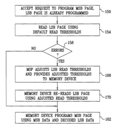
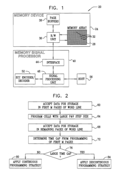
- The implementation of a Memory Signal Processor (MSP) that identifies Discontinuous Programming scenarios and selects appropriate storage strategies, such as modifying programming parameters or using cached data to compute new programming levels, to mitigate error probability and increase programming speed.
Computing-in-memory device including digital-to-analog converter based on memory structure
PatentActiveUS12347520B2
Innovation
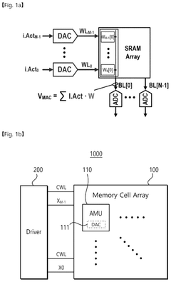
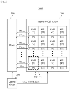
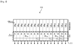
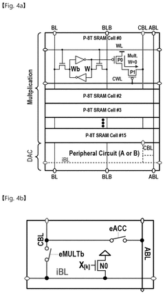
- A computing-in-memory device is developed, which includes a memory cell array with an analog multiplication unit that performs MAC operations on pre-stored weights and multi-bit input data converted into an analog voltage using a digital-to-analog converter (DAC) integrated within the memory.
Power Efficiency Considerations
Power efficiency represents a critical consideration in the development and deployment of multi-bit storage techniques for analog in-memory computing arrays. The fundamental advantage of analog in-memory computing lies in its ability to eliminate the energy-intensive data movement between processing and memory units that plagues conventional von Neumann architectures. However, this advantage can be compromised if the multi-bit storage mechanisms themselves consume excessive power.
Current multi-bit storage implementations face several power-related challenges. The programming operations for precise multi-level states typically require iterative write-verify schemes that consume significant energy compared to binary storage. These operations often involve multiple pulse applications with intermediate verification steps, increasing both programming time and energy consumption. For resistive memory technologies like RRAM and PCM, the SET operations that transition devices to low-resistance states are particularly power-intensive, sometimes requiring current limiting mechanisms to prevent device damage.
The read operations in multi-bit storage systems present another power efficiency concern. Higher precision readout circuits necessary for distinguishing between multiple levels consume more power than binary readout schemes. Additionally, the signal-to-noise ratio requirements for reliable multi-bit storage necessitate higher read currents, further increasing power consumption during operation.
Temperature sensitivity introduces additional power management challenges. Many analog storage elements exhibit temperature-dependent characteristics that affect state retention and read accuracy. Compensation mechanisms, such as temperature sensors and adaptive reference schemes, add to the system's power budget and complexity.
Recent research has focused on several promising approaches to improve power efficiency. Optimized programming algorithms that minimize the number of write-verify iterations while maintaining accuracy have demonstrated energy reductions of 30-50% compared to conventional methods. Novel device structures incorporating selector elements with sharp nonlinear I-V characteristics help reduce sneak path currents in crossbar arrays, significantly decreasing standby power consumption.
Circuit-level innovations include low-power sensing amplifiers specifically designed for multi-bit operations and adaptive programming schemes that adjust pulse parameters based on device characteristics. These approaches have shown potential to reduce read energy by up to 40% while maintaining the required precision for multi-bit storage.
Looking forward, emerging device technologies with inherently lower switching energies, such as ferroelectric FETs and magnetic devices, offer promising pathways to further power efficiency improvements in multi-bit storage systems. The continued development of these technologies, combined with advanced circuit techniques and programming algorithms, will be essential for realizing the full potential of analog in-memory computing arrays in energy-constrained applications.
Reliability and Error Correction Mechanisms
Reliability and error correction mechanisms are critical components in multi-bit storage analog in-memory computing (AIMC) arrays due to the inherent variability and noise susceptibility of analog devices. These mechanisms ensure computational accuracy and system robustness despite the non-ideal characteristics of the physical implementation.
The primary reliability challenges in multi-bit AIMC arrays stem from device-to-device variations, temporal drift, and environmental sensitivity. Device-to-device variations cause inconsistent conductance levels across the array, leading to computational errors. Temporal drift manifests as gradual changes in stored values over time, particularly pronounced in resistive memory technologies like RRAM and PCM. Environmental factors such as temperature fluctuations and power supply variations further exacerbate these reliability issues.
Error correction codes (ECCs) have been adapted specifically for analog memory systems. Unlike traditional digital ECCs, these specialized codes account for the unique error patterns in analog storage. Hamming codes and BCH codes have been modified to handle soft errors in multi-bit cells, while more advanced LDPC codes provide superior error correction capabilities for higher bit precision requirements.
Redundancy techniques represent another approach to error mitigation. Spatial redundancy involves storing multiple copies of critical data across different array locations, while temporal redundancy implements repeated computations with majority voting. These techniques, while effective, come with area and performance overheads that must be carefully balanced against reliability requirements.
Adaptive programming schemes dynamically adjust write parameters based on device characteristics and environmental conditions. These schemes employ closed-loop verification during programming operations, ensuring that target conductance states are achieved despite variability. Some advanced implementations incorporate machine learning algorithms to predict and compensate for device aging effects.
Calibration and compensation techniques address systematic errors in AIMC arrays. Regular calibration routines measure device characteristics and update correction factors stored in lookup tables. These compensation mechanisms can be implemented at various levels, from individual cells to entire arrays, with different granularity-performance tradeoffs.
Error-aware training methodologies have emerged as a promising approach for neural network applications. By incorporating device error models during the training phase, networks can be made inherently robust to the specific error patterns of the underlying hardware. This co-design of algorithms and hardware represents a holistic approach to reliability enhancement in AIMC systems.
Unlock deeper insights with PatSnap Eureka Quick Research — get a full tech report to explore trends and direct your research. Try now!
Generate Your Research Report Instantly with AI Agent
Supercharge your innovation with PatSnap Eureka AI Agent Platform!