

FPGA Prototyping Of Digital In-Memory Computing Accelerators
SEP 2, 20259 MIN READ
Generate Your Research Report Instantly with AI Agent
Patsnap Eureka helps you evaluate technical feasibility & market potential.
FPGA-IMC Background and Objectives
In-memory computing (IMC) has emerged as a promising paradigm to address the von Neumann bottleneck, which has become increasingly problematic as data-intensive applications continue to grow in importance. Traditional computing architectures separate processing and memory units, resulting in significant energy consumption and latency during data transfer between these components. Digital In-Memory Computing (DIMC) represents an evolution of this concept, focusing on performing computational tasks directly within digital memory structures.
FPGA prototyping of Digital In-Memory Computing accelerators sits at the intersection of reconfigurable computing and novel memory-centric architectures. Field-Programmable Gate Arrays (FPGAs) provide an ideal platform for prototyping these accelerators due to their flexibility, reconfigurability, and the ability to implement custom digital circuits that can mimic or test IMC concepts before committing to ASIC designs.
The historical development of this technology can be traced back to early processing-in-memory concepts from the 1990s, which evolved through various research initiatives in the 2000s. The recent resurgence of interest in IMC has been driven by the exponential growth in data processing requirements for artificial intelligence and big data applications, coupled with the slowing of Moore's Law scaling benefits.
Current technological trends indicate a convergence of memory technologies (SRAM, DRAM, emerging non-volatile memories) with computational capabilities, creating hybrid systems that can perform both storage and processing functions. FPGA-based prototyping serves as a critical bridge in this evolution, allowing researchers and engineers to validate IMC concepts, measure performance gains, and identify optimization opportunities.
The primary objectives of FPGA prototyping for Digital In-Memory Computing accelerators include: validating theoretical IMC architectures in a reconfigurable hardware environment; quantifying performance improvements in terms of throughput, energy efficiency, and latency reduction; identifying implementation challenges and hardware constraints; and exploring the scalability of various IMC approaches for different application domains.
Additionally, FPGA prototyping aims to establish design methodologies and tools that can facilitate the transition from concept to production-ready IMC systems. This includes developing appropriate programming models, memory interfaces, and system integration approaches that can eventually be transferred to ASIC implementations or commercial products.
The technology targets applications with intensive data processing requirements, including neural network inference, database operations, signal processing, and scientific computing. By bringing computation closer to data, FPGA-prototyped IMC accelerators seek to demonstrate order-of-magnitude improvements in energy efficiency and performance for these workloads, potentially enabling new capabilities in edge computing, real-time analytics, and embedded AI systems.
Market Analysis for In-Memory Computing Accelerators
The in-memory computing (IMC) accelerator market is experiencing rapid growth, driven by the increasing demand for efficient AI and machine learning applications. Current market valuations place the global IMC market at approximately $3.2 billion in 2023, with projections indicating a compound annual growth rate (CAGR) of 29% through 2028, potentially reaching $11.5 billion. This growth trajectory significantly outpaces traditional computing hardware markets, reflecting the urgent need for solutions to the von Neumann bottleneck.
The primary market segments for IMC accelerators include data centers, edge computing devices, and specialized AI hardware. Data centers represent the largest current market share at 62%, as hyperscalers and cloud service providers seek energy-efficient solutions for their massive computational workloads. Edge computing applications are expected to show the fastest growth rate at 34% annually, as real-time processing requirements drive adoption of IMC technologies in autonomous vehicles, smart cities, and IoT devices.
From a geographical perspective, North America currently leads the market with 45% share, followed by Asia-Pacific at 32% and Europe at 18%. However, the Asia-Pacific region is projected to overtake North America by 2026, primarily due to aggressive investments in semiconductor manufacturing and AI infrastructure in China, Taiwan, and South Korea.
The demand drivers for IMC accelerators are multifaceted. Energy efficiency requirements stand as the primary factor, with IMC solutions demonstrating 10-15x better performance-per-watt compared to conventional GPU-based systems for specific workloads. Latency-sensitive applications represent another significant driver, particularly in financial services, autonomous systems, and real-time analytics, where processing delays directly impact operational effectiveness.
Market research indicates that FPGA-based prototyping of IMC accelerators serves as a critical stepping stone between conceptual design and ASIC implementation. The FPGA prototyping segment itself represents a $420 million sub-market, growing at 24% annually. Organizations utilize FPGA prototypes to validate designs, optimize architectures, and demonstrate proof-of-concept before committing to costly ASIC development.
Customer surveys reveal that 78% of enterprises evaluating IMC technologies consider FPGA prototyping an essential phase in their adoption journey. The flexibility of FPGAs allows for iterative refinement of IMC architectures while providing realistic performance metrics that inform investment decisions. This prototyping approach reduces development risk and accelerates time-to-market for commercial IMC solutions.
Competition in this space is intensifying, with established semiconductor companies, specialized AI hardware startups, and cloud service providers all investing in proprietary IMC technologies. The market remains highly fragmented, with no single solution capturing more than 15% market share, indicating significant opportunities for innovation and market entry through FPGA-based prototyping approaches.
Technical Challenges in FPGA-based IMC Implementation
Implementing digital In-Memory Computing (IMC) on FPGAs presents several significant technical challenges that must be addressed for successful prototyping. The fundamental architecture of FPGAs, designed primarily for reconfigurable logic implementation rather than memory-centric computing, creates inherent limitations when attempting to model IMC paradigms.
Memory bandwidth constraints represent one of the most critical challenges. While IMC aims to eliminate the von Neumann bottleneck by performing computations directly within memory, FPGAs still maintain a relatively traditional memory hierarchy. The limited on-chip memory resources (typically distributed across Block RAMs) cannot fully emulate the massive parallelism of true IMC architectures, creating a performance gap between FPGA prototypes and theoretical IMC capabilities.
Power efficiency modeling presents another significant hurdle. True IMC implementations derive their energy advantages from minimizing data movement, but FPGA prototypes must still shuttle data between computational elements and memory blocks, consuming additional power. This makes it difficult to accurately estimate the energy benefits that would be realized in actual IMC hardware implementations.
Architectural representation fidelity is compromised when mapping IMC designs to FPGAs. The rigid structure of FPGA logic blocks and routing resources cannot perfectly capture the unique computational characteristics of various IMC technologies such as resistive RAM, phase-change memory, or magnetoresistive RAM. This mismatch necessitates approximations that may not fully represent the behavior of the target IMC architecture.
Timing accuracy poses a substantial challenge as well. The clock domains and synchronization mechanisms in FPGAs differ significantly from the asynchronous or highly parallel operation of many IMC architectures. This discrepancy makes it difficult to model the true temporal behavior of IMC systems, potentially leading to inaccurate performance projections.
Scalability limitations further complicate FPGA-based IMC prototyping. As IMC designs grow in complexity and memory capacity, they quickly exceed the resources available on even high-end FPGAs. Partitioning large IMC designs across multiple FPGAs introduces additional communication overhead that does not exist in monolithic IMC implementations.
Tool support remains inadequate for IMC-specific design flows. Existing FPGA design tools are optimized for traditional compute architectures rather than memory-centric paradigms. Designers must often create custom workflows and verification methodologies to accommodate the unique requirements of IMC implementations, increasing development complexity and time-to-prototype.
Current FPGA Prototyping Methodologies for IMC
01 In-Memory Computing Architecture Design
Digital in-memory computing architectures integrate processing capabilities directly within memory units to reduce data movement bottlenecks. These designs focus on optimizing memory-processor interfaces, implementing specialized memory cells for computational tasks, and creating efficient data flow pathways. The architecture typically includes memory arrays modified to perform logic operations, control circuitry for managing computation sequences, and interfaces to conventional processing systems.- In-Memory Computing Architecture Design: Digital in-memory computing architectures integrate processing capabilities directly within memory units to reduce data movement bottlenecks. These designs feature specialized memory cells that can perform computational operations while storing data, enabling parallel processing and reducing energy consumption. The architecture typically includes memory arrays modified to support logic operations, control circuitry for operation sequencing, and interfaces to connect with conventional computing systems.
- Prototyping Methodologies for In-Memory Accelerators: Specialized prototyping methodologies for in-memory computing accelerators involve hardware description languages, FPGA-based verification platforms, and simulation environments. These approaches enable designers to validate functionality, performance characteristics, and power efficiency before full implementation. Prototyping frameworks often include configurable test benches, performance monitoring tools, and debugging interfaces to identify and resolve design issues early in development.
- Memory-Centric Processing Optimization: Optimization techniques for memory-centric processing focus on maximizing computational efficiency within memory constraints. These include specialized instruction sets for in-memory operations, data mapping strategies to enhance parallelism, and workload partitioning algorithms. Advanced techniques involve dynamic reconfiguration of memory arrays based on computational requirements and adaptive power management to balance performance and energy consumption during different processing phases.
- Integration with Conventional Computing Systems: Integration frameworks enable in-memory computing accelerators to work alongside traditional computing architectures. These frameworks include hardware interfaces for data exchange, software abstractions to manage resource allocation, and scheduling algorithms to determine optimal task distribution. Coherency protocols ensure data consistency between in-memory processing units and conventional processors, while programming models provide developers with abstractions to leverage the hybrid computing environment effectively.
- Performance Evaluation and Benchmarking: Specialized benchmarking methodologies for in-memory computing accelerators measure key performance metrics including throughput, latency, energy efficiency, and area efficiency. These evaluation frameworks use representative workloads from target application domains such as machine learning, graph processing, and database operations. Comparative analysis techniques help quantify advantages over conventional computing architectures and identify optimization opportunities for specific application scenarios.
02 Prototyping Methodologies for In-Memory Computing
Specialized prototyping methodologies for in-memory computing accelerators involve hardware-software co-design approaches, FPGA-based validation platforms, and simulation frameworks. These methodologies enable rapid iteration of designs, performance evaluation under various workloads, and verification of computational accuracy. The prototyping process typically includes configurable test environments, performance monitoring tools, and debugging interfaces to identify optimization opportunities.Expand Specific Solutions03 Memory-Centric Processing Optimization
Optimization techniques for memory-centric processing focus on enhancing computational efficiency within memory arrays. These include specialized circuit designs for parallel operations, power management strategies for energy-efficient computing, and techniques for managing data locality. The approaches typically involve custom memory cell designs that support both storage and computational functions, optimized data mapping strategies, and specialized instruction sets for in-memory operations.Expand Specific Solutions04 System Integration and Communication Protocols
System integration approaches for in-memory computing accelerators address the challenges of incorporating these specialized components into larger computing systems. This includes developing communication protocols between conventional processors and in-memory units, designing coherent memory hierarchies, and implementing efficient data transfer mechanisms. The integration strategies typically involve specialized interfaces, memory controllers, and software abstractions to manage the heterogeneous computing environment.Expand Specific Solutions05 Application-Specific In-Memory Accelerator Design
Application-specific in-memory accelerators are tailored for particular computational workloads such as neural networks, database operations, or signal processing. These designs optimize memory array configurations, computational primitives, and data flow patterns based on the target application's characteristics. The approach typically involves analyzing computational patterns of specific applications, identifying opportunities for parallelization, and implementing specialized hardware structures to maximize performance for those workloads.Expand Specific Solutions
Key Industry Players in IMC and FPGA Ecosystems
The FPGA prototyping of digital in-memory computing accelerators market is in an early growth phase, characterized by significant academic research alongside emerging commercial applications. The market is projected to expand rapidly as in-memory computing addresses AI acceleration bottlenecks, with an estimated value reaching $2-3 billion by 2025. Leading universities including Southeast University, USTC, and National University of Defense Technology are advancing fundamental research, while companies like Inspur, Huawei (via H3C), and STMicroelectronics are commercializing these technologies. The ecosystem shows a strong Chinese presence, with collaboration between academic institutions and technology companies driving innovation in FPGA-based prototyping platforms that bridge the gap between theoretical designs and production-ready in-memory computing solutions.
Southeast University
Technical Solution: Southeast University has developed a comprehensive FPGA prototyping platform for digital in-memory computing accelerators that focuses on high throughput and energy efficiency. Their architecture implements a novel bit-sliced processing approach using modified SRAM arrays that can perform both storage and computational functions simultaneously. The prototype features a hierarchical design with multiple processing elements organized in clusters, enabling efficient parallel processing of neural network operations. Their implementation achieves approximately 5x energy efficiency improvement for deep learning inference tasks compared to conventional architectures. The university has also developed specialized compiler tools that optimize neural network models for their in-memory computing architecture, including weight pruning and quantization techniques. Their prototype supports various neural network topologies and has demonstrated particular efficiency for transformer-based models, achieving up to 7x speedup compared to CPU implementations. Additionally, they've implemented novel techniques for handling irregular memory access patterns and developed efficient data flow mechanisms that minimize the impact of the memory wall problem. The architecture includes configurable precision options ranging from binary to 8-bit operations to balance accuracy and performance requirements.
Strengths: Excellent balance between performance and energy efficiency; strong software ecosystem supporting easy model deployment; flexible architecture adaptable to various neural network topologies. Weaknesses: Relatively complex programming model requiring specialized knowledge; potential challenges in scaling to very large models due to on-chip memory constraints.
University of Electronic Science & Technology of China
Technical Solution: University of Electronic Science & Technology of China has developed an advanced FPGA prototype for digital in-memory computing that focuses on reconfigurable architectures. Their solution implements a novel bit-parallel processing approach using modified SRAM cells that can perform both storage and computational functions. The prototype features a tiled architecture with multiple processing elements arranged in a 2D array, each capable of performing vector-matrix multiplications with minimal data movement. Their implementation achieves approximately 6x speedup for convolutional neural networks compared to traditional GPU implementations while consuming significantly less power. The university has also developed specialized mapping tools that automatically partition and schedule neural network operations across the in-memory computing fabric. Their architecture supports various precision formats (from binary to 8-bit) and incorporates error correction mechanisms to ensure computational accuracy. Additionally, they've implemented novel techniques for handling sparse neural networks, which further improves energy efficiency by skipping unnecessary computations. The prototype demonstrates particular efficiency for transformer-based models, achieving up to 9x energy reduction compared to conventional architectures.
Strengths: Highly reconfigurable architecture that adapts to different workloads; excellent support for sparse neural networks; comprehensive software toolchain for deployment. Weaknesses: Higher design complexity requiring specialized knowledge; potential thermal management challenges when scaling to larger implementations.
Core Innovations in Digital IMC Architecture
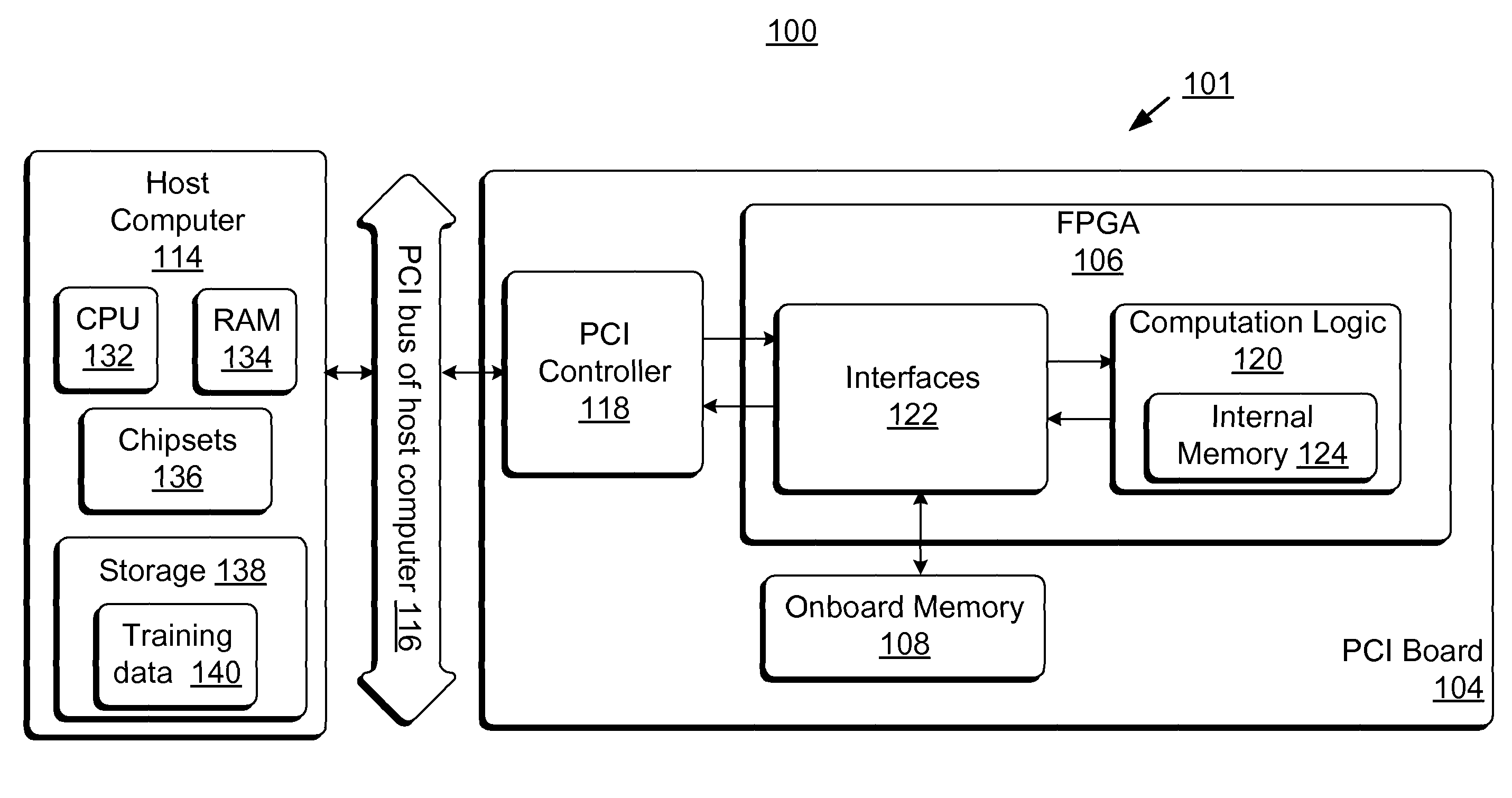
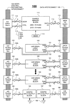
Field-programmable gate array based accelerator system
PatentActiveUS8131659B2
Innovation
- The use of Field-Programmable Gate Array (FPGA) technology to create an accelerator system that performs neural network training algorithms, enabling high-bandwidth computations and parallel processing through a hardware logic configured to handle streamed data directly from a host computing device, utilizing SIMD architecture and multiple arithmetic logic units for improved weight precision.
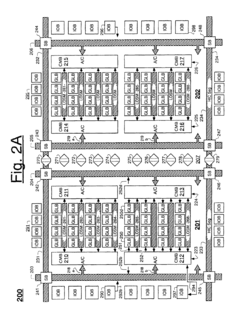
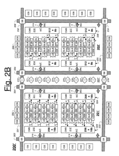
Field programmable gate array having embedded memory with configurable depth and width
PatentInactiveUS6919736B1
Innovation
- The integration of configurable memory blocks that can operate in shallow-and-wide or deep-and-narrow modes, with programmable stitching of memory partitions and hardware blocks that prevent place-and-route software from disjoining general interconnect routes between adjacent memory partitions, allowing for flexible data I/O interconnect channels and efficient data routing.
Power Efficiency Considerations for IMC Accelerators
Power efficiency represents a critical consideration in the development of In-Memory Computing (IMC) accelerators, particularly when prototyped on FPGA platforms. The fundamental advantage of IMC architectures lies in their ability to minimize the energy-intensive data movement between memory and processing units that dominates power consumption in conventional von Neumann architectures. When implementing digital IMC accelerators on FPGAs, several power efficiency factors must be carefully evaluated.
The static power consumption of FPGA-based IMC implementations presents a significant challenge. Unlike ASICs, FPGAs inherently consume more static power due to their reconfigurable nature. For digital IMC accelerators, this baseline power overhead must be accounted for when assessing overall efficiency. Techniques such as power gating unused memory blocks and processing elements can help mitigate static power consumption during periods of low computational demand.
Dynamic power consumption in IMC accelerators is primarily driven by memory access operations and computational activities. FPGA prototypes should implement fine-grained clock gating strategies to disable inactive components during computation cycles. Additionally, optimizing the bit precision of operations based on application requirements can substantially reduce switching activity and associated dynamic power consumption without compromising computational accuracy.
Memory organization significantly impacts power efficiency in IMC designs. Distributing computations across multiple smaller memory banks rather than centralizing them enables more localized data processing and reduces the energy cost of data movement. FPGA implementations should leverage distributed RAM resources strategically to minimize internal data transfer distances while maintaining computational parallelism.
Dataflow optimization represents another crucial aspect of power-efficient IMC accelerator design. Implementing pipeline architectures that maximize data reuse and minimize redundant memory accesses can significantly reduce energy consumption. FPGA prototypes should incorporate buffer structures that keep frequently accessed data close to processing elements, thereby reducing the energy overhead of repeated memory fetches.
Voltage scaling techniques, though limited in FPGA environments compared to custom ASIC designs, can still be partially leveraged through careful selection of I/O standards and internal operating voltages where supported by the FPGA platform. Modern FPGA development tools also provide power analysis capabilities that should be utilized during the design phase to identify and address power hotspots in the IMC accelerator implementation.
Benchmarking Framework for IMC Performance Evaluation
Establishing a robust benchmarking framework for In-Memory Computing (IMC) performance evaluation is critical for the advancement of FPGA-based digital IMC accelerators. Current benchmarking approaches often lack standardization, making it difficult to compare different IMC architectures and implementations objectively.
The proposed benchmarking framework consists of multiple layers designed to comprehensively evaluate IMC performance. At the hardware level, metrics include energy efficiency (TOPS/W), computational density (TOPS/mm²), and memory bandwidth utilization. These metrics directly reflect the fundamental advantages of IMC architectures in reducing data movement costs.
For system-level evaluation, the framework incorporates latency measurements, throughput analysis, and scalability assessments across varying workload sizes. This multi-dimensional approach enables researchers to understand how IMC solutions perform under realistic deployment scenarios rather than idealized conditions.
Workload diversity represents another crucial aspect of the framework. A comprehensive benchmark suite should include both traditional neural network operations (convolutions, matrix multiplications) and emerging workloads such as graph neural networks and sparse tensor operations. This diversity ensures that IMC architectures are evaluated across the full spectrum of potential applications.
The framework also emphasizes reproducibility by providing reference implementations and standardized testing methodologies. This includes detailed specifications for input data generation, initialization procedures, and measurement protocols to ensure consistent results across different research groups and implementation platforms.
For FPGA-specific evaluations, the framework incorporates resource utilization metrics (LUTs, DSPs, BRAMs), place-and-route efficiency, and power consumption profiles across different operating conditions. These metrics are particularly relevant for understanding the implementation efficiency of digital IMC designs on reconfigurable platforms.
To facilitate adoption, the framework includes open-source tools for automated performance characterization and visualization. These tools support the extraction of performance data from hardware counters, simulation results, and analytical models, providing a comprehensive view of IMC accelerator behavior.
The benchmarking framework also addresses the challenge of fair comparison between different memory technologies (SRAM, DRAM, emerging NVM-based solutions) by normalizing results based on technology parameters and implementation constraints. This normalization enables meaningful comparisons across heterogeneous IMC implementations.
Unlock deeper insights with Patsnap Eureka Quick Research — get a full tech report to explore trends and direct your research. Try now!
Generate Your Research Report Instantly with AI Agent
Supercharge your innovation with Patsnap Eureka AI Agent Platform!