

Device-To-Architecture Co-Design In Phase-Change In-Memory Computing
SEP 2, 20259 MIN READ
Generate Your Research Report Instantly with AI Agent
Patsnap Eureka helps you evaluate technical feasibility & market potential.
PCM Computing Background and Objectives
Phase-change memory (PCM) computing represents a revolutionary paradigm in the landscape of computing architectures, emerging from the convergence of memory and processing capabilities. The evolution of PCM technology dates back to the 1960s when Stanford Ovshinsky first discovered the phase-change phenomenon in chalcogenide materials. However, it wasn't until the early 2000s that significant advancements in material science and fabrication techniques propelled PCM into practical applications.
The technological trajectory of PCM has been characterized by continuous improvements in switching speed, endurance, and energy efficiency. Initially developed as a non-volatile memory solution, PCM has evolved beyond simple storage to become a promising platform for in-memory computing, addressing the fundamental bottleneck in von Neumann architectures—the separation of memory and processing units.
Current trends in PCM development focus on multi-level cell capabilities, 3D integration, and enhanced reliability through novel material compositions. The integration of PCM with conventional CMOS technology has opened pathways for hybrid computing systems that leverage the strengths of both technologies.
The primary objective of device-to-architecture co-design in PCM computing is to optimize the entire computing stack—from material properties and device physics to circuit design and system architecture—in a holistic manner. This approach aims to maximize computational efficiency while minimizing energy consumption, a critical consideration in the era of data-intensive applications and edge computing.
Specific technical goals include developing PCM cells with improved resistance contrast, faster switching speeds, and enhanced endurance for computational operations. At the architectural level, objectives encompass creating efficient mapping strategies for neural network operations, developing specialized instruction sets for in-memory computing, and designing scalable interconnect solutions for large-scale PCM arrays.
The long-term vision for PCM computing extends to neuromorphic applications, where the inherent properties of phase-change materials—particularly their ability to emulate synaptic behavior—could enable more efficient implementation of artificial neural networks and brain-inspired computing paradigms.
As we advance toward exascale computing and beyond, PCM-based in-memory computing represents a promising approach to overcome the energy and performance limitations of conventional architectures, potentially enabling new classes of applications in artificial intelligence, scientific computing, and real-time data analytics.
Market Analysis for In-Memory Computing Solutions
The in-memory computing (IMC) market is experiencing rapid growth, driven by the increasing demand for high-performance computing solutions across various industries. The global IMC market was valued at approximately $2.5 billion in 2022 and is projected to reach $9.8 billion by 2028, representing a compound annual growth rate (CAGR) of 25.6%. This growth is primarily fueled by the exponential increase in data generation and the need for real-time processing capabilities.
Phase-change memory (PCM) based in-memory computing solutions are gaining significant traction within this market due to their unique advantages in terms of non-volatility, scalability, and multi-level cell capabilities. The PCM segment of the IMC market is expected to grow at a CAGR of 29.3% through 2028, outpacing other memory technologies.
Key application areas driving market demand include artificial intelligence, machine learning, big data analytics, and edge computing. The AI/ML segment alone accounts for approximately 38% of the total IMC market, with financial services, healthcare, and telecommunications being the primary vertical industries adopting these solutions.
Geographically, North America currently holds the largest market share at 42%, followed by Asia-Pacific at 31% and Europe at 21%. However, the Asia-Pacific region is expected to witness the highest growth rate over the forecast period, primarily due to increasing investments in AI infrastructure and digital transformation initiatives in countries like China, South Korea, and Japan.
The demand for PCM-based IMC solutions is particularly strong in applications requiring low-power operation and high computational density. Edge computing applications are expected to represent the fastest-growing segment, with a projected CAGR of 34.2% through 2028, as organizations increasingly process data closer to the source to reduce latency and bandwidth usage.
Customer requirements are evolving toward integrated solutions that combine hardware acceleration with specialized software frameworks. End-users are seeking systems that can deliver 10-100x performance improvements over conventional computing architectures while maintaining energy efficiency. The total cost of ownership (TCO) has become a critical factor in adoption decisions, with organizations expecting ROI within 18-24 months of deployment.
Market challenges include competition from alternative technologies such as resistive RAM (ReRAM) and magnetoresistive RAM (MRAM), as well as concerns regarding standardization and integration with existing computing infrastructures. However, the unique advantages of PCM in terms of endurance, retention, and multi-level cell capabilities position it favorably in the competitive landscape.
Technical Challenges in PCM In-Memory Computing
Phase-Change Memory (PCM) in-memory computing faces several significant technical challenges that impede its widespread adoption and commercial viability. The non-linear and stochastic behavior of PCM devices presents a fundamental obstacle, as these characteristics introduce variability in computational results, affecting accuracy and reliability. This variability stems from cycle-to-cycle variations during programming operations and device-to-device differences due to manufacturing inconsistencies.
The endurance limitation of PCM devices represents another critical challenge. Current PCM technologies typically support 10^6 to 10^8 write cycles before failure, which falls short of the requirements for intensive computing applications that demand billions of operations. This limitation necessitates sophisticated wear-leveling techniques and error correction mechanisms, adding complexity to system design.
Power consumption remains a significant concern in PCM-based computing systems. The high current required for phase transitions, particularly during the SET operation (crystallization), can lead to substantial energy consumption. This challenge becomes particularly acute in large-scale arrays where numerous cells operate simultaneously, potentially negating the energy efficiency advantages that in-memory computing promises.
Scaling issues present multifaceted challenges for PCM technology. As device dimensions shrink to accommodate higher density requirements, thermal crosstalk between adjacent cells becomes more pronounced, potentially causing unintended phase changes in neighboring cells. Additionally, smaller cell sizes result in reduced programming volumes, exacerbating variability concerns and reliability issues.
The integration of PCM with CMOS technology introduces complex design considerations. The voltage and current requirements for PCM operations often differ significantly from standard CMOS logic levels, necessitating specialized interface circuits. Furthermore, the thermal budget constraints during fabrication must accommodate both technologies, adding manufacturing complexity.
Architectural challenges extend beyond device-level concerns. Designing efficient data mapping schemes that optimize the utilization of PCM arrays while minimizing write operations requires sophisticated algorithms. Additionally, developing programming schemes that balance accuracy, speed, and energy efficiency represents a complex optimization problem that remains partially solved.
The lack of standardized design methodologies and tools specifically tailored for PCM-based computing systems further complicates development efforts. Current electronic design automation (EDA) tools are primarily optimized for conventional computing architectures, creating a gap in the design ecosystem for novel in-memory computing paradigms based on PCM technology.
Current Device-Architecture Co-Design Approaches
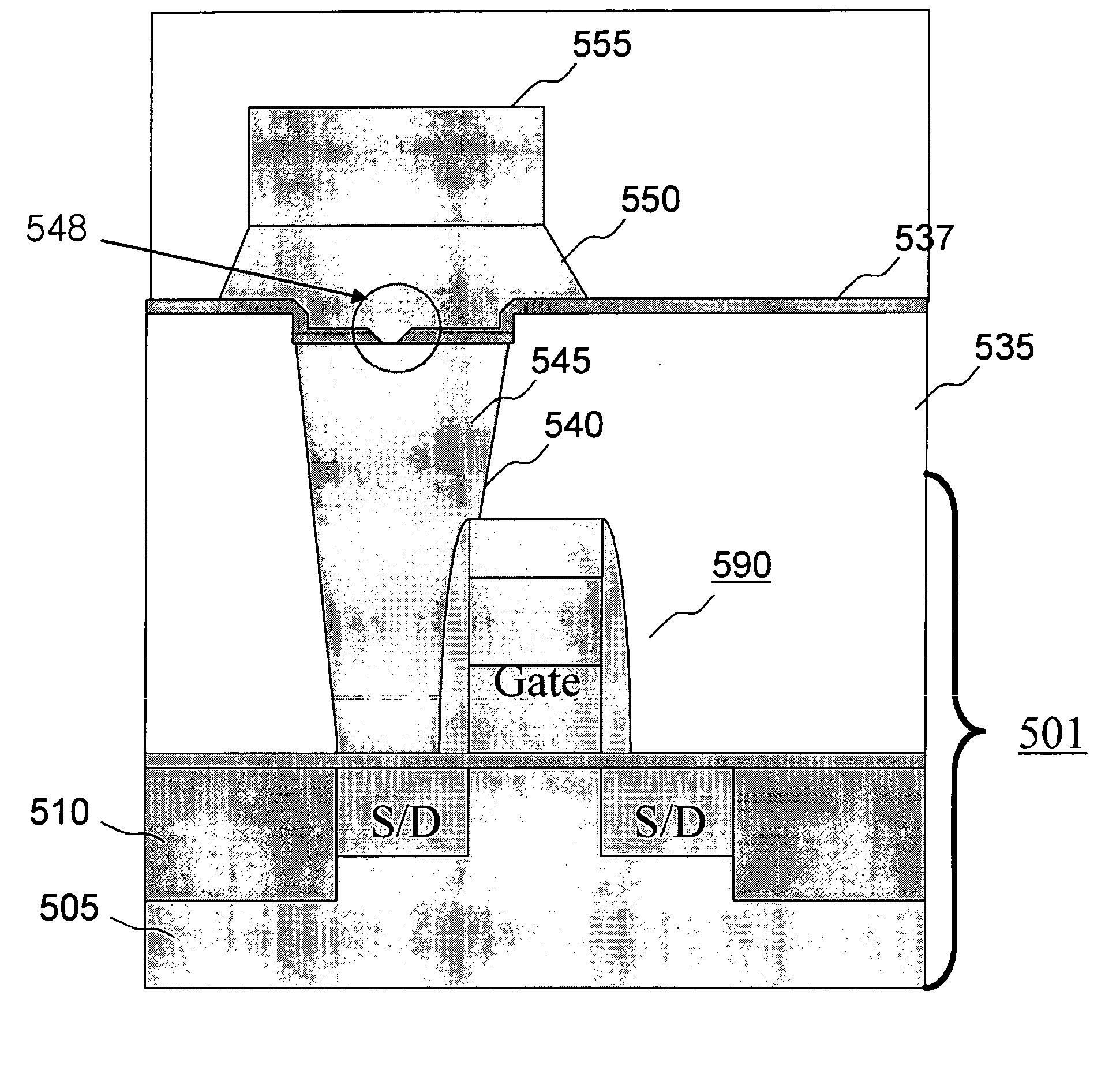
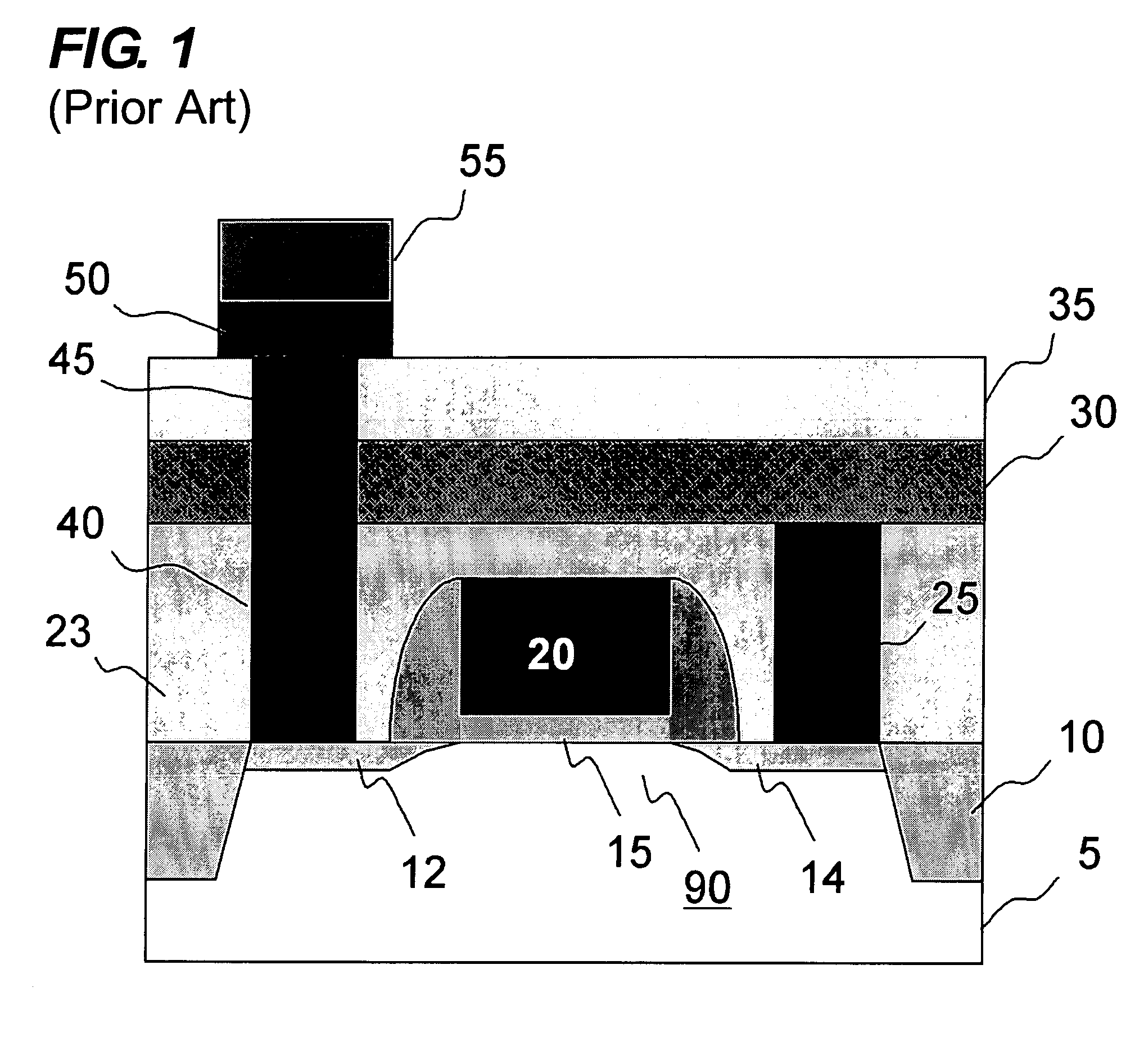
01 Phase-change memory device structures
Phase-change memory devices utilize specific structural designs to optimize performance and functionality. These structures include various electrode configurations, cell geometries, and material interfaces that affect the phase transition process. The designs focus on improving thermal efficiency, reducing power consumption, and enhancing reliability of the phase-change process. Advanced structural elements such as confined cell architectures and multi-layer electrode arrangements enable better control over the phase-change mechanism.- Phase-change memory device structures: Phase-change memory devices utilize specific structural designs to optimize performance and functionality. These structures include various electrode configurations, cell geometries, and material interfaces that affect the phase transition process. The designs focus on improving thermal efficiency, reducing power consumption, and enhancing reliability of the phase-change process. Key structural innovations include confined cell architectures, multi-layer electrode designs, and specialized contact interfaces that control heat distribution during programming operations.
- Memory architecture and integration techniques: Integration of phase-change memory into computing architectures requires specialized design approaches that address the unique characteristics of these devices. This includes developing memory arrays, addressing schemes, and peripheral circuitry optimized for phase-change operation. The architecture designs focus on efficient data access patterns, reduced latency, and improved scalability. Integration techniques also address challenges related to thermal management, signal integrity, and compatibility with existing semiconductor manufacturing processes.
- In-memory computing implementations: In-memory computing leverages phase-change materials to perform computational tasks directly within the memory array, reducing data movement between processing and storage units. These implementations utilize the analog nature of phase-change materials to enable operations such as matrix multiplication, neural network processing, and logic functions. The designs focus on creating efficient computational primitives that exploit the resistance states of phase-change materials, enabling parallel processing capabilities while minimizing energy consumption and improving computational density.
- Material innovations for phase-change memory: Advanced materials play a crucial role in optimizing phase-change memory performance for computing applications. Material innovations focus on chalcogenide compounds with tailored properties, including modified crystallization temperatures, switching speeds, and retention characteristics. These materials are engineered to provide multi-level resistance states, improved endurance, and reduced drift in resistance values over time. Doping strategies and compositional tuning are employed to enhance specific properties required for in-memory computing applications.
- Co-design methodologies and system optimization: Co-design methodologies integrate device-level characteristics with architectural considerations to create optimized phase-change memory computing systems. These approaches involve simultaneous optimization of circuit designs, programming algorithms, and system architectures based on the physical properties of phase-change materials. The methodologies address challenges such as variability management, error correction, and performance-energy tradeoffs. System-level optimizations include specialized instruction sets, memory controllers, and programming models that leverage the unique capabilities of phase-change memory for computational tasks.
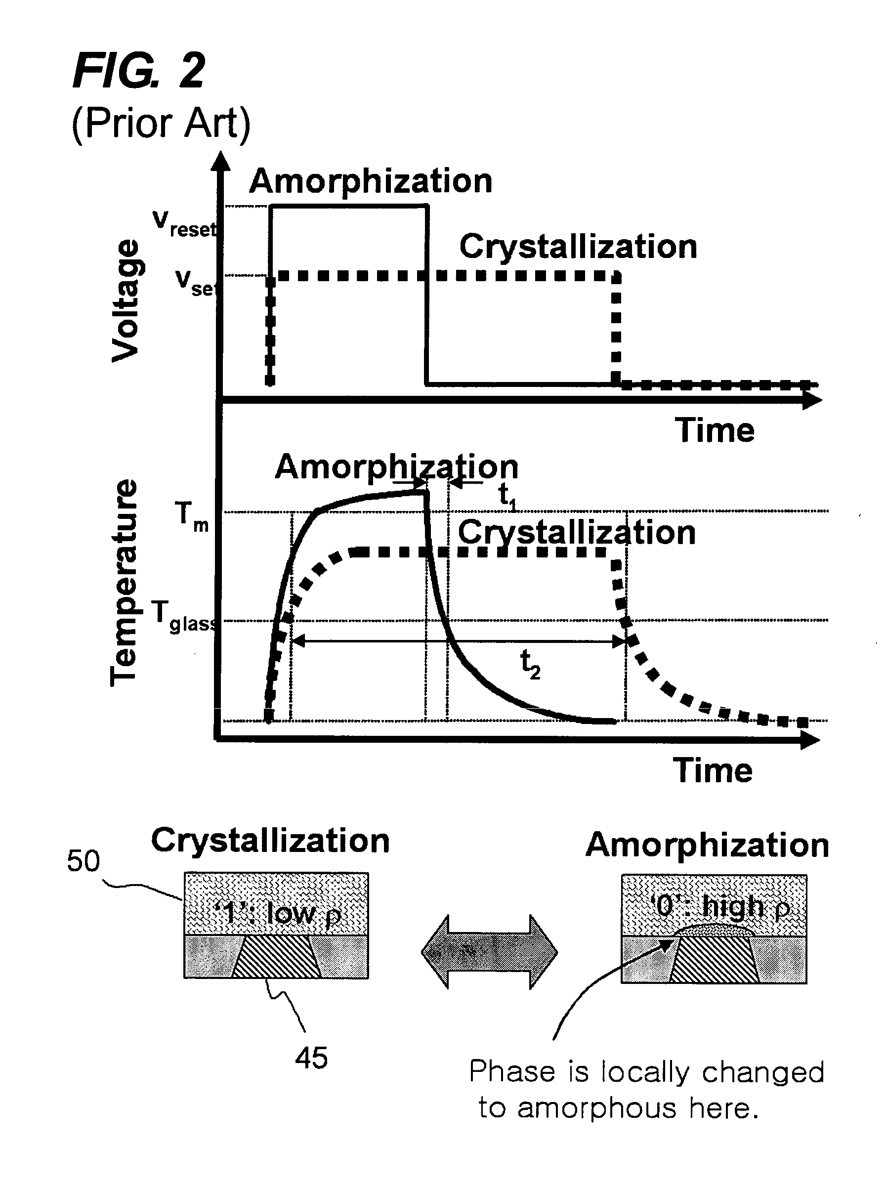
02 Memory operation and control mechanisms
Specialized control mechanisms are implemented to manage the operation of phase-change memory devices. These include programming algorithms that control the heating and cooling rates during phase transitions, read operations that detect resistance states, and verification schemes that ensure reliable data storage. Advanced control techniques incorporate pulse shaping, current regulation, and temperature management to optimize the phase-change process and extend device endurance.Expand Specific Solutions03 Integration with computing architectures
Phase-change memory devices are designed to integrate with various computing architectures to enable in-memory computing capabilities. This co-design approach involves creating memory structures that can perform computational tasks directly within the memory array, reducing data movement between memory and processing units. The integration includes interface designs, addressing schemes, and signal processing elements that allow phase-change memory to function both as storage and as computational elements in neuromorphic, logic-in-memory, and other novel computing paradigms.Expand Specific Solutions04 Material composition and engineering
The performance of phase-change memory devices heavily depends on the composition and engineering of phase-change materials. Research focuses on developing materials with optimal crystallization speed, thermal stability, and resistance contrast between amorphous and crystalline states. Advanced material engineering includes doping strategies, interface engineering, and multi-compound formulations to enhance switching characteristics, reduce power consumption, and improve endurance. Chalcogenide-based materials, particularly germanium-antimony-tellurium (GST) compounds, are commonly used with various modifications to achieve desired performance metrics.Expand Specific Solutions05 Novel computing paradigms and applications
Phase-change memory enables novel computing paradigms beyond traditional von Neumann architectures. These include neuromorphic computing systems that mimic brain functionality, in-memory computing that performs calculations directly within memory arrays, and hybrid computing approaches that combine the advantages of different memory technologies. Applications range from artificial intelligence acceleration to edge computing and Internet of Things devices, where the non-volatile nature and computational capabilities of phase-change memory provide significant advantages in terms of power efficiency and processing speed.Expand Specific Solutions
Key Industry Players in PCM Computing
The phase-change in-memory computing (PCM) market is currently in a growth stage, characterized by increasing research activities and commercial interest. The global market for this technology is expanding, driven by demands for more efficient computing architectures for AI and big data applications. Technologically, PCM is advancing toward maturity with key players like IBM, Samsung, and SK Hynix leading research and development efforts. IBM has established a strong patent portfolio in device-to-architecture co-design approaches, while Samsung and TSMC are leveraging their semiconductor manufacturing expertise to scale PCM solutions. Academic institutions such as KAIST and industrial collaborations with companies like Micron Technology and Macronix are accelerating innovation in this field. The technology shows promise for commercial viability, though challenges in manufacturing scalability and system integration remain.
International Business Machines Corp.
Technical Solution: IBM has pioneered phase-change in-memory computing (PCM) through their device-to-architecture co-design approach. Their solution integrates phase-change memory materials (typically Ge2Sb2Te5) with specialized computing architectures to perform computations directly within memory, eliminating the von Neumann bottleneck. IBM's PCM technology enables multi-level cell storage by precisely controlling crystallization states, allowing analog computation for AI workloads. Their architecture incorporates peripheral circuitry specifically designed to handle the unique characteristics of PCM devices, including programming current control and read sensing schemes. IBM has demonstrated PCM-based neural networks achieving 200x energy efficiency improvements compared to conventional computing approaches[1]. Their co-design methodology addresses reliability challenges through error correction techniques and redundancy schemes tailored to PCM's specific wear-out mechanisms and variability characteristics[3].
Strengths: Industry-leading expertise in PCM materials science and integration; extensive patent portfolio; demonstrated neural network implementations with significant energy efficiency gains. Weaknesses: PCM endurance limitations still present challenges for write-intensive applications; temperature sensitivity requires additional compensation circuitry, increasing complexity.
Samsung Electronics Co., Ltd.
Technical Solution: Samsung has developed a comprehensive device-to-architecture co-design approach for phase-change in-memory computing focused on vertical integration. Their solution incorporates proprietary chalcogenide materials with optimized switching characteristics and specialized peripheral circuits designed to maximize computational efficiency. Samsung's architecture features a crossbar array structure with selector devices that minimize sneak path currents, enabling higher density and improved parallel computing capabilities. Their PCM technology implements precision programming algorithms that achieve up to 8 distinct resistance levels per cell, significantly enhancing the computational density for neural network applications[5]. Samsung has also pioneered 3D stacking techniques for PCM devices, increasing storage density while maintaining computational capabilities. Their co-design approach includes specialized sensing circuits that compensate for device-to-device variations and drift effects, improving the reliability of in-memory computing operations over extended periods[7].
Strengths: Vertical integration from materials to systems provides complete solution control; manufacturing expertise enables high-volume production; advanced 3D integration capabilities. Weaknesses: Higher power consumption compared to some competing technologies; resistance drift over time requires complex compensation algorithms that add computational overhead.
Critical Patents and Research in PCM Co-Design
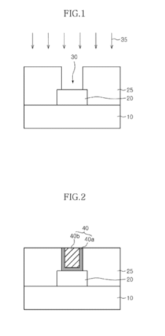
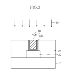
Phase-change memory device and manufacturing method thereof
PatentInactiveUS20050018526A1
Innovation
- A method involving the formation of a lower electrode with a surrounding dielectric layer, a thin dielectric layer with a micro pore or damaged spot to create a localized current path, and depositing phase-change material to fill the pore or damaged spot, simplifying the process and enhancing productivity.
Phase-change memory device and method of fabricating the same
PatentActiveUS8802536B2
Innovation
- A phase-change memory device is fabricated using a semiconductor substrate with a first material-rich phase-change layer formed along the inner surface of the phase-change area via atomic layer deposition, followed by a second phase-change layer deposited using a Ge-Sb-Te material to enhance coating uniformity and deposition selectivity, ensuring uniform filling of the phase-change area.

Energy Efficiency and Performance Benchmarking
Phase-change memory (PCM) based in-memory computing architectures represent a significant advancement in addressing the von Neumann bottleneck. When evaluating these systems, energy efficiency and performance metrics serve as critical benchmarks for determining their viability in real-world applications. Current PCM-based computing solutions demonstrate remarkable energy efficiency advantages compared to conventional computing architectures, with some implementations achieving 10-100x improvements in energy consumption for specific computational tasks.
Performance benchmarking of PCM-based in-memory computing systems reveals varying efficiency across different computational workloads. Matrix-vector multiplications and neural network inference operations show particularly promising results, with energy consumption as low as 0.3-2 pJ per multiply-accumulate operation in optimized architectures. This efficiency stems from the elimination of data movement between separate memory and processing units, which typically accounts for 60-80% of energy consumption in traditional computing systems.
Systematic benchmarking methodologies have been developed specifically for phase-change in-memory computing, incorporating metrics such as computational density (operations per unit area), energy-delay product, and throughput under various operating conditions. These frameworks enable fair comparisons between different device-architecture combinations and highlight the trade-offs between performance parameters.
Temperature sensitivity remains a significant challenge in PCM-based systems, with performance metrics showing notable variation across operating temperature ranges. Recent co-design approaches have implemented adaptive programming schemes that adjust programming parameters based on temperature feedback, maintaining consistent performance across varying environmental conditions.
Endurance considerations also impact long-term energy efficiency, as resistance drift in PCM cells necessitates periodic refresh operations that consume additional energy. Advanced co-design strategies incorporate wear-leveling algorithms and optimized refresh schedules that minimize the energy overhead while maintaining computational accuracy over extended operational periods.
Scaling analysis indicates that energy efficiency improvements become more pronounced as the technology scales down, with projected efficiency gains of up to 1000x for large-scale matrix operations in future implementations. However, these projections depend heavily on successful mitigation of device-level challenges such as cell-to-cell variability and resistance drift.
Comparative analysis against competing technologies, including RRAM and MRAM-based computing architectures, positions PCM-based solutions favorably in applications requiring high precision and moderate operating speeds, while other technologies may offer advantages in ultra-low power or high-speed domains.
Manufacturing Scalability and Integration Challenges
Phase-change in-memory computing faces significant manufacturing scalability and integration challenges that must be addressed for widespread commercial adoption. Current fabrication processes for phase-change memory (PCM) devices require precise control of material deposition, particularly for the chalcogenide materials like Ge2Sb2Te5 (GST) that form the active switching medium. The integration of these materials with CMOS processes presents compatibility issues, as PCM fabrication typically requires higher temperatures than standard CMOS back-end-of-line processes can tolerate.
The scaling of PCM cells to smaller dimensions introduces additional manufacturing complexities. As device dimensions shrink below 20nm, the thermal confinement necessary for efficient programming becomes increasingly difficult to maintain. This results in higher programming currents relative to cell size, creating challenges for power efficiency and thermal management. Furthermore, the variability in switching characteristics increases at smaller nodes, affecting the reliability and uniformity of computational operations in in-memory computing applications.
Integration density represents another critical challenge. While PCM offers higher density than SRAM, achieving the integration levels necessary for complex in-memory computing architectures requires advanced 3D stacking techniques. Current manufacturing capabilities limit the number of PCM layers that can be reliably stacked, constraining the overall computational capacity of these systems. The yield rates for multi-layer PCM arrays remain significantly lower than those for conventional memory technologies.
The co-design approach necessitates close collaboration between device engineers and architecture designers, creating organizational challenges in manufacturing environments where these teams traditionally operate separately. Establishing effective communication channels and shared design tools between these groups is essential but often difficult to implement in practice. This interdisciplinary requirement extends to manufacturing processes, where equipment and methodologies must be adapted to support the unique requirements of device-architecture co-optimized designs.
Cost considerations further complicate the manufacturing landscape. The specialized materials and processing steps required for PCM fabrication currently result in higher per-bit costs compared to conventional memory technologies. Economic viability demands either cost reduction through manufacturing innovation or the targeting of high-value applications where the computational benefits outweigh the cost premium. The industry is actively pursuing both paths, with significant research focused on process simplification and material alternatives.
Unlock deeper insights with Patsnap Eureka Quick Research — get a full tech report to explore trends and direct your research. Try now!
Generate Your Research Report Instantly with AI Agent
Supercharge your innovation with Patsnap Eureka AI Agent Platform!