

What Challenges Limit Large-Scale Adoption Of In-Memory Computing Processors
SEP 2, 20259 MIN READ
Generate Your Research Report Instantly with AI Agent
PatSnap Eureka helps you evaluate technical feasibility & market potential.
In-Memory Computing Evolution and Objectives
In-memory computing (IMC) represents a paradigm shift in computer architecture that addresses the von Neumann bottleneck by integrating computation and memory functions within the same physical space. This technology has evolved significantly over the past decades, transitioning from theoretical concepts to practical implementations across various computing platforms.
The evolution of in-memory computing began in the 1990s with early research into computational memory structures. By the early 2000s, researchers had developed primitive processing-in-memory (PIM) architectures that demonstrated the potential for significant performance improvements in specific applications. The mid-2010s marked a turning point with the emergence of commercially viable resistive RAM (ReRAM), phase-change memory (PCM), and magnetoresistive RAM (MRAM) technologies that enabled more sophisticated in-memory computing capabilities.
Recent advancements have focused on developing specialized in-memory computing processors for artificial intelligence applications, particularly neural network inference and training. These processors leverage analog computing principles to perform matrix multiplications directly within memory arrays, dramatically reducing energy consumption and increasing computational throughput for AI workloads.
The primary objective of in-memory computing research is to overcome the memory wall—the growing disparity between processor and memory speeds that limits overall system performance. By eliminating data movement between separate processing and memory units, IMC aims to achieve orders-of-magnitude improvements in energy efficiency and computational density for data-intensive applications.
Additional technical objectives include developing scalable architectures that maintain computational accuracy across large arrays, creating programming models that abstract hardware complexities, and designing hybrid systems that effectively combine traditional and in-memory computing paradigms. Researchers are also working to extend the application scope of IMC beyond AI to include database operations, scientific computing, and real-time signal processing.
The long-term vision for in-memory computing encompasses fully integrated heterogeneous computing systems where different computational tasks are dynamically assigned to the most appropriate computing substrate—whether traditional CPUs, GPUs, or various forms of in-memory processors. This approach promises to deliver unprecedented performance and energy efficiency for next-generation computing applications, from edge devices to data centers.
As the technology continues to mature, the focus is increasingly shifting toward addressing practical implementation challenges while maintaining the fundamental advantages that make in-memory computing a promising solution for the post-Moore's Law computing era.
Market Analysis for In-Memory Computing Solutions
The in-memory computing (IMC) processor market has experienced significant growth in recent years, driven by increasing demands for real-time data processing and analytics. The global market for IMC solutions was valued at approximately $2.3 billion in 2022 and is projected to reach $6.7 billion by 2027, representing a compound annual growth rate (CAGR) of 23.8%. This growth trajectory reflects the expanding application landscape across various industries seeking to overcome traditional von Neumann architecture bottlenecks.
Financial services represent the largest market segment, accounting for nearly 30% of IMC adoption. Banks and financial institutions leverage these solutions for real-time fraud detection, risk assessment, and algorithmic trading where microsecond advantages translate to significant competitive edges. The telecommunications sector follows closely at 22% market share, utilizing IMC for network optimization, customer experience management, and real-time service quality monitoring.
Healthcare and life sciences constitute a rapidly growing segment (18% market share) where IMC accelerates genomic sequencing, drug discovery simulations, and patient data analytics. Manufacturing and retail sectors collectively represent approximately 15% of the market, implementing IMC for supply chain optimization and real-time inventory management.
Geographically, North America leads adoption with 42% market share, followed by Europe (28%) and Asia-Pacific (23%). The Asia-Pacific region demonstrates the highest growth rate at 27.3% CAGR, driven by China's aggressive investments in semiconductor technologies and artificial intelligence infrastructure.
Market analysis reveals several key demand drivers. First, the exponential growth in data volume and velocity necessitates processing architectures that eliminate memory-processor bottlenecks. Second, the proliferation of edge computing applications requires low-latency, energy-efficient computing solutions that IMC can provide. Third, advancements in AI and machine learning algorithms demand computational frameworks capable of handling complex matrix operations efficiently.
Customer pain points primarily center around integration complexity with existing systems, concerns regarding data persistence during power failures, and the high initial investment costs. The total cost of ownership remains a significant barrier, with IMC solutions typically commanding a 40-60% premium over traditional computing architectures.
The competitive landscape features established players like IBM, Intel, and Samsung alongside specialized startups such as Mythic, Syntiant, and GrAI Matter Labs. Recent market consolidation through acquisitions signals industry maturation, with larger semiconductor companies acquiring innovative startups to expand their IMC portfolios.
Technical Barriers and Global Development Status
In-memory computing processors face significant technical barriers that hinder their widespread adoption. The integration of memory and processing units on the same chip introduces complex thermal management challenges. As computational density increases, heat dissipation becomes problematic, potentially causing performance degradation and reliability issues. Current cooling technologies struggle to efficiently manage heat in these densely packed architectures, limiting operational frequencies and overall system performance.
Power consumption remains another critical barrier. Despite promising energy efficiency for specific workloads, in-memory computing processors often require substantial power during intensive operations. This creates challenges for deployment in energy-constrained environments such as edge devices and mobile platforms, where battery life and thermal constraints are paramount considerations.
Manufacturing complexity presents substantial obstacles to mass production. The fabrication of hybrid memory-processing elements demands specialized processes that differ from conventional CMOS manufacturing. This results in lower yields, higher production costs, and difficulties in scaling to high-volume production. The need for precise integration of memory materials with logic circuits requires advanced fabrication techniques that are not yet fully mature for commercial-scale implementation.
Programming models and software ecosystems for in-memory computing remain underdeveloped. Traditional computing paradigms and programming languages are designed for the von Neumann architecture, creating a significant gap in developer tools and frameworks optimized for in-memory computing. This software barrier impedes adoption as organizations face steep learning curves and substantial code refactoring requirements to leverage these new architectures effectively.
Globally, research and development in in-memory computing processors show geographic concentration. North America leads in fundamental research and startup innovation, with companies like IBM and Mythic pioneering commercial applications. Europe contributes significantly to theoretical advancements and algorithm development, particularly through research institutions in Switzerland, Germany, and the Netherlands.
The Asia-Pacific region, especially China, South Korea, and Japan, demonstrates growing investment in manufacturing capabilities and application-specific implementations. These countries are rapidly developing expertise in materials science and fabrication techniques essential for in-memory computing. However, a notable development gap exists between research prototypes and commercially viable products across all regions.
Standardization efforts remain fragmented, with competing architectural approaches and no clear consensus on evaluation metrics or benchmarking methodologies. This fragmentation complicates technology assessment and investment decisions, further slowing industry-wide adoption despite promising research outcomes.
Current Architectural Approaches and Implementations
01 In-Memory Processing Architecture
In-memory computing processors utilize architectures where processing occurs directly within memory units, eliminating the traditional bottleneck of data transfer between memory and CPU. This approach significantly reduces latency and power consumption while increasing computational throughput for data-intensive applications. These architectures integrate processing elements with memory arrays, enabling parallel operations on large datasets without moving data through conventional memory hierarchies.- Architecture and design of in-memory computing processors: In-memory computing processors are designed with specialized architectures that integrate processing capabilities directly within memory units, reducing data movement between memory and processing units. These architectures enable parallel processing of data, significantly improving computational efficiency for data-intensive applications. Key design elements include memory cell arrays that can perform logical and arithmetic operations, specialized interconnects, and control logic that manages data flow within the memory structure.
- Performance optimization techniques for in-memory processors: Various techniques are employed to optimize the performance of in-memory computing processors for large-scale adoption. These include advanced memory management algorithms, data compression methods, and specialized instruction sets designed for in-memory operations. Additionally, techniques such as pipelining, caching strategies specific to in-memory architectures, and power management optimizations help balance computational efficiency with energy consumption, making these processors more viable for widespread commercial deployment.
- Integration with existing computing infrastructure: For large-scale adoption, in-memory computing processors must integrate seamlessly with existing computing infrastructure. This involves developing compatible interfaces with standard memory buses, creating software frameworks that abstract the complexity of in-memory computing, and ensuring compatibility with popular programming models. Solutions include hybrid architectures that combine traditional processing with in-memory capabilities, middleware that facilitates communication between in-memory systems and conventional software, and standardized APIs for application development.
- Application-specific optimizations for data-intensive workloads: In-memory computing processors are being optimized for specific data-intensive applications to drive large-scale adoption. These optimizations include specialized circuits for machine learning operations, database query acceleration, and real-time analytics. By tailoring the architecture to specific computational patterns found in these applications, in-memory processors can achieve orders of magnitude improvements in performance and energy efficiency compared to conventional architectures, making them particularly attractive for industries dealing with massive datasets.
- Scalability and manufacturing considerations: Large-scale adoption of in-memory computing processors depends on addressing scalability and manufacturing challenges. This includes developing fabrication techniques compatible with existing semiconductor manufacturing processes, designing architectures that can scale from small embedded systems to large data centers, and creating fault-tolerance mechanisms to handle the reliability issues inherent in dense memory arrays. Innovations in 3D stacking, non-volatile memory technologies, and defect-tolerant designs are helping overcome these challenges to enable mass production and deployment.
02 Scalability Solutions for Enterprise Deployment
Large-scale adoption of in-memory computing processors requires robust scalability solutions. These include distributed memory management systems, dynamic resource allocation mechanisms, and fault-tolerance protocols that maintain system reliability as deployments grow. Enterprise-grade implementations incorporate load balancing algorithms and memory virtualization techniques to efficiently handle varying workloads across multiple nodes while maintaining consistent performance.Expand Specific Solutions03 Energy Efficiency and Thermal Management
Advanced energy efficiency techniques are critical for widespread adoption of in-memory computing processors in data centers. These include dynamic voltage and frequency scaling, selective power gating of inactive memory regions, and intelligent thermal management systems. Optimized memory access patterns and specialized cooling solutions help maintain operational stability while reducing overall power consumption, making large-scale deployments economically viable.Expand Specific Solutions04 Software Frameworks and Programming Models
Specialized software frameworks and programming models facilitate the adoption of in-memory computing processors by abstracting hardware complexities. These frameworks provide high-level APIs, memory-aware compilers, and runtime systems that automatically optimize code for in-memory execution. Development tools support parallel programming paradigms and data locality optimizations, enabling efficient utilization of in-memory architectures without requiring extensive hardware knowledge from application developers.Expand Specific Solutions05 Integration with AI and Big Data Workloads
In-memory computing processors are increasingly optimized for artificial intelligence and big data analytics workloads, driving their large-scale adoption. These processors incorporate specialized matrix operation units, tensor processing capabilities, and graph traversal accelerators directly within memory structures. Such integrations enable real-time processing of massive datasets for machine learning training and inference, natural language processing, and complex analytics that would be prohibitively slow with conventional computing architectures.Expand Specific Solutions
Leading Companies and Competitive Landscape
In-memory computing processors are currently in a transitional phase from early adoption to mainstream implementation, with the market expected to grow significantly as data processing demands increase. Technical maturity varies considerably across key players, with established semiconductor giants like Intel, IBM, and Micron leading commercial deployment, while companies such as NeuroBlade, Cambricon, and Synthara drive innovation in specialized architectures. Academic institutions including Tsinghua University and University of Michigan contribute fundamental research. Major adoption challenges include memory density limitations, power consumption concerns, software ecosystem fragmentation, and high implementation costs, creating a competitive landscape where companies must balance performance gains against practical deployment considerations.
Intel Corp.
Technical Solution: Intel has developed Optane DC Persistent Memory, a groundbreaking in-memory computing solution that bridges the gap between DRAM and storage. This technology creates a new memory tier that offers near-DRAM performance with storage-like capacity and persistence. Intel's approach combines specialized hardware with software optimizations through their Persistent Memory Development Kit (PMDK), enabling applications to directly access persistent memory as memory-mapped files. Their architecture addresses key challenges by providing data persistence during power loss events, significantly larger memory capacity than traditional DRAM (up to 512GB per module), and backward compatibility with existing systems. Intel has also focused on security enhancements with hardware-level encryption to protect data at rest, addressing confidentiality concerns in memory-centric architectures.
Strengths: Intel's solution offers an established ecosystem with strong software support and compatibility with existing x86 architectures. Their memory modules provide exceptional capacity-to-performance ratio compared to traditional DRAM. Weaknesses: Higher cost compared to conventional memory solutions, thermal management challenges at scale, and performance that, while impressive, still doesn't fully match DRAM speeds for all workloads.
NeuroBlade Ltd.
Technical Solution: NeuroBlade has developed a novel computational storage processor called XRAM that fundamentally reimagines in-memory computing by bringing computation directly to where data resides. Their architecture integrates thousands of processing cores alongside memory arrays on the same silicon die, creating a massively parallel processing engine that eliminates the traditional data movement bottleneck. NeuroBlade's solution particularly targets big data analytics workloads, where it claims performance improvements of 10-100x compared to conventional architectures. The company's technology employs a specialized instruction set optimized for data-intensive operations and includes a software stack that allows seamless integration with popular analytics frameworks like Apache Spark. Their approach addresses scaling challenges through a modular design that can be deployed from edge devices to data center racks, with each processing element handling a portion of the dataset locally.
Strengths: NeuroBlade's architecture dramatically reduces energy consumption by minimizing data movement, achieves exceptional parallelism for data-intensive workloads, and maintains software compatibility through intelligent abstraction layers. Weaknesses: Limited applicability outside analytics workloads, relatively new technology with less established ecosystem support, and potential challenges with programming model complexity for developers unfamiliar with their architecture.
Key Patents and Research Breakthroughs
In-memory computing processor, processing system, processing apparatus, deployment method of algorithm model
PatentPendingUS20230168891A1
Innovation
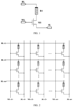
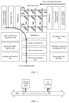
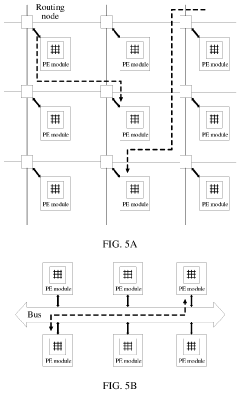
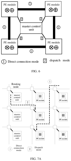
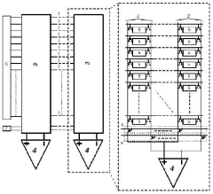
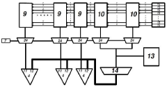
- The development of an in-memory computing processor with a hybrid dispatch architecture, comprising a master control unit and memristor processing modules that can calculate independently and communicate directly, supporting multiple computing modes such as direct connection, dispatch, and hybrid modes to optimize data interaction and reduce latency and power consumption.
A flash ADC based method and process for in-memory computation
PatentActiveIN202041033411A
Innovation
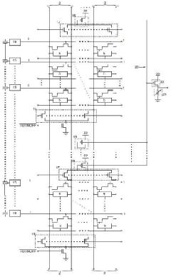
- A modified SRAM array is partitioned into weight and reference data-lines, with internally generated reference voltages transmitted through a multiplexer to a sense amplifier for parallel comparison, using a single ADC for all data-lines to reduce space and power consumption.
Power Efficiency and Thermal Management Challenges
Power efficiency and thermal management represent critical barriers to the widespread adoption of in-memory computing (IMC) processors. These processors, which integrate computation directly within memory arrays, inherently consume significant power due to their architectural design. The power consumption challenge stems from the high density of computational elements and memory cells operating simultaneously, creating substantial energy demands that exceed those of conventional von Neumann architectures in many implementations.
Current IMC designs face a fundamental trade-off between computational throughput and power efficiency. While moving computation to memory eliminates energy-intensive data movement, the parallel operation of numerous computing elements within memory arrays generates considerable heat. This thermal concentration creates hotspots that can compromise reliability, reduce component lifespan, and necessitate sophisticated cooling solutions that increase system complexity and cost.
The thermal management challenge is particularly acute in high-performance applications where IMC processors must sustain intensive computational workloads. Without adequate thermal solutions, these processors must operate at reduced clock frequencies or implement aggressive power throttling, significantly undermining their performance advantages. This limitation becomes especially problematic in data centers and edge computing environments where power budgets are strictly constrained.
Material limitations further compound these challenges. Current semiconductor materials used in IMC implementations exhibit thermal conductivity properties that impede efficient heat dissipation from densely packed computational elements. This physical constraint necessitates innovative cooling approaches beyond traditional heat sink and fan combinations, potentially including liquid cooling or phase-change materials that add complexity to system design.
Power delivery networks for IMC processors must also manage substantial current fluctuations during operation. The simultaneous activation of numerous computational units creates power demand spikes that stress voltage regulators and distribution networks. These transient power behaviors necessitate sophisticated power management circuitry that adds overhead to both chip area and energy consumption.
From a system integration perspective, the thermal and power challenges of IMC processors complicate their incorporation into existing computing infrastructures. Data centers and enterprise environments have established cooling and power distribution systems optimized for conventional processors, requiring significant modifications to accommodate the different thermal and power profiles of IMC architectures. This integration barrier represents a substantial hurdle for organizations considering large-scale IMC deployment.
Standardization and Ecosystem Development
The lack of standardization in the in-memory computing (IMC) processor industry represents a significant barrier to widespread adoption. Currently, each IMC solution operates within its proprietary ecosystem, creating fragmentation that complicates integration into existing technology stacks. This absence of unified standards affects hardware interfaces, programming models, and software development frameworks, forcing potential adopters to commit to specific vendor ecosystems with limited interoperability.
Hardware standardization remains particularly challenging, with diverse architectures ranging from resistive RAM to phase-change memory implementations. These varied approaches create incompatible physical interfaces and communication protocols, preventing the development of universal hardware integration methods. The resulting vendor lock-in concerns discourage many organizations from making substantial investments in IMC technology.
Software ecosystem limitations compound these challenges. The absence of standardized programming abstractions forces developers to learn vendor-specific languages and tools, significantly increasing development costs and technical debt. Most IMC solutions lack robust software development kits, debugging tools, and comprehensive documentation, creating steep learning curves that deter adoption even when the underlying technology shows promise.
Industry collaboration initiatives have emerged but remain insufficient. Several consortia have attempted to establish common frameworks, but competing commercial interests have slowed meaningful progress. The fragmented standardization efforts themselves create uncertainty about which standards might eventually prevail, causing many potential adopters to delay implementation decisions until clearer industry direction emerges.
Academic-industry partnerships represent a potential pathway forward, with several university research programs working alongside commercial entities to develop open reference architectures. These collaborations aim to create vendor-neutral specifications that could serve as de facto standards. However, these efforts require broader industry participation and commitment to succeed at scale.
The ecosystem challenge extends to the talent pipeline. The specialized knowledge required for IMC development is not widely taught in computer science curricula, creating a shortage of qualified engineers and researchers. This talent gap further constrains ecosystem development, as organizations struggle to find personnel capable of implementing and maintaining IMC solutions regardless of standardization progress.
Unlock deeper insights with PatSnap Eureka Quick Research — get a full tech report to explore trends and direct your research. Try now!
Generate Your Research Report Instantly with AI Agent
Supercharge your innovation with PatSnap Eureka AI Agent Platform!