

Latency Reduction Techniques In SRAM-Based In-Memory Computing Arrays
SEP 2, 20259 MIN READ
Generate Your Research Report Instantly with AI Agent
Patsnap Eureka helps you evaluate technical feasibility & market potential.
SRAM-Based IMC Evolution and Objectives
SRAM-based In-Memory Computing (IMC) has evolved significantly over the past decade, transforming from a theoretical concept to a practical solution addressing the von Neumann bottleneck. The evolution began in the early 2010s with rudimentary analog computing capabilities integrated into SRAM arrays, primarily focusing on simple multiply-accumulate operations for neural network acceleration.
By mid-2010s, researchers achieved notable breakthroughs in circuit design, enabling more complex operations within memory arrays while maintaining reasonable power consumption. This period marked the transition from proof-of-concept prototypes to functional test chips demonstrating tangible performance advantages for specific workloads.
The evolution accelerated around 2018-2020 with the introduction of hybrid digital-analog computing architectures that improved precision and reliability while preserving the latency benefits of in-memory computation. These developments coincided with the exponential growth in AI applications, creating a perfect technological convergence.
Current SRAM-based IMC technologies have reached a maturity level where they can deliver 10-100x improvements in energy efficiency and significant latency reductions compared to conventional computing architectures for specific workloads. However, they still face challenges in terms of precision, scalability, and programming model complexity.
The primary objective of latency reduction in SRAM-based IMC arrays is to minimize data movement between processing and memory units, which constitutes the fundamental bottleneck in conventional computing architectures. By performing computations directly within memory arrays, these systems aim to achieve sub-nanosecond operation latencies for critical computational kernels.
Secondary objectives include improving energy efficiency by eliminating redundant data transfers, enhancing scalability to support larger models and datasets, and maintaining compatibility with existing software frameworks to facilitate adoption.
Looking forward, the technology trajectory suggests continued refinement of circuit techniques to reduce peripheral overhead, development of more sophisticated in-memory operations beyond basic vector-matrix multiplications, and integration with emerging memory technologies to overcome current density and retention limitations.
The ultimate goal is to create a versatile computing platform that can dynamically adapt between conventional computing modes and in-memory computing modes based on workload characteristics, providing optimal performance across diverse applications while maintaining programmability and compatibility with existing software ecosystems.
Market Demand for Low-Latency Computing Solutions
The demand for low-latency computing solutions has experienced exponential growth across multiple sectors, driven primarily by the increasing complexity of computational tasks and the emergence of time-sensitive applications. In data centers, where milliseconds can translate to millions in revenue loss, the push for reduced latency has become a strategic imperative. Financial institutions implementing high-frequency trading algorithms require processing speeds measured in nanoseconds to maintain competitive advantage, creating a premium market segment for ultra-low-latency solutions.
Edge computing applications represent another significant market driver, with IDC projecting the global edge computing market to reach $250 billion by 2024. The proliferation of IoT devices—expected to surpass 75 billion connected units by 2025—necessitates processing capabilities that minimize data transfer delays. Autonomous vehicles, smart cities, and industrial automation systems all demand real-time processing to ensure operational safety and efficiency.
The artificial intelligence and machine learning sector has emerged as perhaps the most voracious consumer of low-latency computing resources. Training complex neural networks and executing inference operations in real-time applications have pushed traditional computing architectures to their limits. This has catalyzed interest in specialized hardware solutions, including SRAM-based in-memory computing arrays that can significantly reduce the data movement bottleneck.
Healthcare applications present another growing market segment, with medical imaging, real-time patient monitoring, and surgical robotics all requiring minimal processing delays. The telemedicine market, accelerated by recent global events, demands solutions that can process and transmit high-definition video and sensor data with imperceptible latency.
Market analysis indicates that companies are willing to invest substantially in technologies that reduce computational latency. A recent survey of enterprise technology decision-makers revealed that 78% consider latency reduction a high or critical priority for their infrastructure investments over the next three years. This willingness to invest is reflected in the premium pricing sustainable for solutions that demonstrably reduce processing delays.
The telecommunications sector's transition to 5G and eventually 6G networks further amplifies demand for low-latency computing solutions. Network infrastructure must process vast data volumes with minimal delay to deliver on the promise of sub-millisecond latency for next-generation applications. This creates significant opportunities for SRAM-based in-memory computing arrays that can serve as accelerators within the network infrastructure.
Current Challenges in SRAM-Based IMC Latency
SRAM-based In-Memory Computing (IMC) arrays face significant latency challenges that impede their widespread adoption in high-performance computing systems. The fundamental issue stems from the inherent trade-off between computational density and operational speed. As more computing elements are integrated within memory arrays, the parasitic capacitance and resistance increase proportionally, leading to longer charging and discharging times for bitlines and wordlines.
One critical challenge is the analog-to-digital conversion (ADC) bottleneck. In SRAM-based IMC architectures, computation results often need conversion from analog to digital domains, introducing substantial latency overhead. Current ADC implementations consume significant power and occupy considerable chip area, creating a performance bottleneck that can account for up to 60% of the total operational latency in some IMC designs.
Peripheral circuit delays present another major challenge. The sense amplifiers, write drivers, and control logic surrounding the SRAM array contribute to latency through signal propagation delays. These components must be carefully designed to minimize delay while maintaining reliability, creating complex engineering trade-offs that are difficult to optimize simultaneously.
Voltage scaling limitations further exacerbate latency issues. While reducing operating voltage could potentially decrease switching times, SRAM cells become increasingly unstable at lower voltages due to process variations. This stability-performance trade-off restricts the minimum operational voltage, thereby limiting potential latency improvements through voltage scaling techniques.
Process variation effects introduce unpredictable latency variations across the array. Manufacturing inconsistencies cause threshold voltage variations among transistors, resulting in non-uniform access times across different cells within the same array. This variability necessitates conservative timing margins, effectively increasing overall latency to accommodate worst-case scenarios.
Thermal management challenges also impact latency performance. As computational density increases, power density rises correspondingly, leading to localized heating. These thermal hotspots degrade transistor performance and increase leakage current, both of which contribute to increased operational latency. Current thermal management solutions add complexity and can themselves introduce additional latency overhead.
The interconnect architecture between SRAM cells represents another significant latency challenge. As array sizes scale up, the length and complexity of interconnects increase, adding resistance and capacitance to signal paths. This RC delay becomes increasingly dominant in larger arrays, creating a fundamental scaling limitation for SRAM-based IMC systems seeking to minimize latency while maximizing computational capacity.
Current Latency Reduction Methodologies
01 Architectural designs to reduce latency in SRAM-based computing arrays
Various architectural designs can be implemented to reduce latency in SRAM-based in-memory computing arrays. These designs include optimized memory hierarchies, parallel processing structures, and specialized circuit configurations that minimize data movement between memory and processing units. By integrating computation directly within the memory array, these architectures significantly reduce the time required for data transfer, thereby decreasing overall latency in computational tasks.- Architectural designs for reducing latency in SRAM-based computing arrays: Various architectural designs can be implemented to reduce latency in SRAM-based in-memory computing arrays. These designs include optimized memory cell structures, improved sense amplifiers, and specialized circuit configurations that enable faster data processing within the memory array. By integrating computational elements directly into the memory structure, these architectures minimize data movement between memory and processing units, significantly reducing access latency and improving overall system performance.
- Parallel processing techniques in SRAM-based computing: Parallel processing techniques can be employed in SRAM-based in-memory computing arrays to reduce latency. These techniques involve simultaneous execution of multiple operations across different memory cells or arrays, enabling more efficient data processing. By leveraging the inherent parallelism of memory arrays, computational tasks can be distributed and executed concurrently, significantly reducing the overall processing time and improving system throughput for complex operations.
- Advanced memory access protocols for latency reduction: Advanced memory access protocols can be implemented to reduce latency in SRAM-based in-memory computing arrays. These protocols optimize how data is read from and written to memory cells, reducing the time required for memory operations. Techniques such as burst mode access, pipelining, and predictive fetching can be employed to streamline data flow and minimize wait times. These protocols are particularly effective when combined with specialized hardware that supports rapid memory addressing and efficient data transfer.
- Circuit-level optimizations for SRAM computing arrays: Circuit-level optimizations can significantly reduce latency in SRAM-based in-memory computing arrays. These optimizations include enhanced sense amplifiers, reduced bit-line capacitance, and improved voltage regulation circuits. By fine-tuning the electrical characteristics of memory cells and peripheral circuits, the time required for read, write, and computational operations can be minimized. Additionally, specialized circuit designs that support analog computing within digital memory structures can enable more efficient execution of certain algorithms directly within the memory array.
- Integration of processing elements within SRAM arrays: Integrating processing elements directly within SRAM arrays can substantially reduce latency in in-memory computing systems. This approach places computational units in close proximity to memory cells, minimizing the physical distance that data needs to travel. By embedding logic gates, arithmetic units, or even more complex processors within the memory structure, operations can be performed where the data resides rather than transferring it to external processing units. This integration eliminates the traditional memory bottleneck and enables faster execution of data-intensive applications.
02 Advanced memory cell designs for in-memory computing
Specialized SRAM cell designs can enhance in-memory computing performance by reducing latency. These designs incorporate additional transistors or modified circuit topologies that enable computational operations directly within the memory cells. By performing computations where data is stored, these advanced cell designs eliminate the need to move data to separate processing units, significantly reducing latency for operations such as vector multiplication, neural network inference, and other data-intensive tasks.Expand Specific Solutions03 Pipeline optimization techniques for SRAM-based computing
Pipeline optimization techniques can be employed to reduce latency in SRAM-based in-memory computing arrays. These techniques include instruction-level parallelism, data prefetching, and optimized scheduling algorithms that maximize throughput while minimizing idle cycles. By carefully orchestrating the flow of data and operations through the computing array, these pipeline optimizations can significantly reduce the overall latency of computational tasks performed within SRAM structures.Expand Specific Solutions04 Power management strategies to improve latency
Power management strategies can be implemented to improve latency in SRAM-based in-memory computing arrays. These strategies include dynamic voltage and frequency scaling, selective activation of memory blocks, and power-aware scheduling algorithms. By optimizing power consumption, these techniques can reduce thermal constraints and allow for higher operating frequencies, thereby decreasing computational latency while maintaining energy efficiency in SRAM-based computing systems.Expand Specific Solutions05 Novel sensing and computing mechanisms for SRAM arrays
Novel sensing and computing mechanisms can be integrated into SRAM arrays to reduce latency in in-memory computing applications. These mechanisms include analog computing elements, specialized sense amplifiers, and bit-line computing circuits that enable computational operations to be performed during the memory access cycle. By leveraging these innovative sensing techniques, SRAM-based computing arrays can execute complex operations with significantly reduced latency compared to conventional memory-processor architectures.Expand Specific Solutions
Key Industry Players in IMC Technology
The in-memory computing SRAM array latency reduction market is currently in a growth phase, with increasing demand driven by AI and edge computing applications. The market is expected to reach significant scale as companies address power and performance constraints in data-intensive applications. Leading semiconductor manufacturers like Micron, Intel, TSMC, and Samsung are advancing the technology, while specialized players such as Everspin Technologies and Encharge AI focus on innovative memory architectures. Research institutions including Huazhong University of Science & Technology and Tsinghua University contribute fundamental breakthroughs. The technology is approaching commercial maturity with several companies demonstrating working prototypes, though challenges in scaling and integration remain before widespread adoption.
Micron Technology, Inc.
Technical Solution: Micron has developed advanced SRAM-based in-memory computing arrays that incorporate several latency reduction techniques. Their Compute-in-Memory (CiM) architecture integrates computation directly within SRAM arrays, eliminating data movement between memory and processing units. Micron's implementation uses a hybrid approach combining analog and digital computing within SRAM cells, allowing for parallel vector-matrix multiplications directly in memory. Their technology employs specialized sensing circuits with reduced bit-line capacitance and optimized voltage margins to decrease sensing delays. Additionally, Micron has implemented hierarchical bit-line structures and segmentation techniques that reduce the effective capacitance of bit-lines, significantly decreasing charging and discharging times during read/write operations. Their latest designs incorporate dynamic voltage scaling that adjusts operating voltages based on workload requirements, optimizing the power-performance tradeoff while maintaining low latency for critical operations.
Strengths: Micron's solutions excel in energy efficiency by minimizing data movement, achieving up to 10x reduction in energy consumption compared to conventional architectures. Their hybrid analog-digital approach provides flexibility across different workloads. Weaknesses: The analog computing components may suffer from precision limitations and are susceptible to process variations and temperature fluctuations, potentially requiring additional calibration circuits.
International Business Machines Corp.
Technical Solution: IBM has pioneered several innovative approaches to reduce latency in SRAM-based in-memory computing arrays. Their Phase-Change Memory (PCM) and SRAM hybrid architecture combines the density advantages of PCM with the speed of SRAM for accelerating AI workloads. For pure SRAM-based solutions, IBM has developed an advanced in-memory computing architecture that implements bit-line computing techniques with analog multiplication directly within memory arrays. Their design incorporates specialized peripheral circuits that enable parallel multiply-accumulate operations across multiple SRAM columns simultaneously. IBM's latency reduction techniques include adaptive sensing schemes that dynamically adjust sensing time based on data patterns, reducing average read latency. They've also implemented hierarchical word-line structures that decrease word-line RC delay and improve access times. Additionally, IBM has developed specialized circuit techniques to mitigate bit-line noise and improve sensing margins, allowing for faster and more reliable read operations even at lower operating voltages.
Strengths: IBM's solutions demonstrate excellent scalability and can be integrated with existing CMOS manufacturing processes. Their hybrid architectures provide flexibility across different workloads and memory requirements. Weaknesses: The complexity of IBM's designs may lead to increased manufacturing costs and potential yield issues. Some of their analog computing approaches may face challenges with precision and reproducibility across different operating conditions.
Critical Patents in SRAM-Based IMC Optimization
Area-efficient scalable memory read-data multiplexing and latching
PatentActiveUS20230137508A1
Innovation
- The implementation of a 2-to-1 multiplexor and an interruptible latch in a midblock, along with a complementary tristatable driver, allows for efficient multiplexing and latching of read-data from SRAM blocks, reducing the number of logic gates and eliminating pre-charging requirements, thereby improving power and area efficiency.
Memory HUB and access method having internal row caching
PatentWO2004013897A2
Innovation
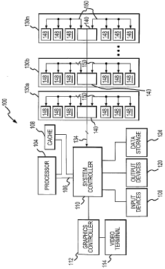
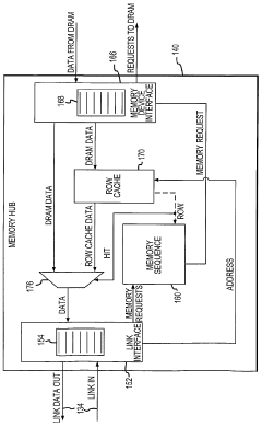
- A memory hub architecture with a link interface, memory device interface, and a row cache memory that stores read data and generates memory requests to reduce latency, allowing for efficient data transfer and cache coherency through a sequencer that manages access to memory cells and pre-fetches data from memory devices.
Power-Latency Tradeoffs in IMC Architectures
In-Memory Computing (IMC) architectures inherently face a fundamental trade-off between power consumption and operational latency. This relationship represents one of the most critical design considerations when implementing SRAM-based IMC arrays. The power-latency balance directly impacts both the energy efficiency and computational throughput of these systems, ultimately determining their viability for various applications.
Traditional SRAM-based IMC designs often prioritize either power efficiency or speed, rarely achieving optimal performance in both dimensions simultaneously. When optimizing for reduced latency, techniques such as parallel computing, higher operating voltages, and aggressive sensing schemes are typically employed. However, these approaches invariably lead to increased power consumption, sometimes exponentially so, particularly when operating at near-threshold or sub-threshold voltage levels.
Conversely, power-optimized IMC architectures implement techniques like voltage scaling, power gating, and reduced precision computing. While these methods effectively reduce energy consumption, they typically introduce additional delays in computation cycles, thereby increasing overall latency. This inverse relationship creates a design space where architects must carefully position their solutions based on application requirements.
Recent research has explored several promising approaches to navigate this trade-off more effectively. Adaptive voltage scaling techniques allow dynamic adjustment of operating parameters based on computational workload, enabling systems to shift along the power-latency curve as needed. Similarly, hybrid architectures that combine different memory technologies (e.g., SRAM for latency-critical operations and non-volatile memory for power-critical functions) offer another pathway to balance these competing demands.
The application context significantly influences the optimal power-latency balance. Edge computing devices with strict energy constraints may favor power efficiency at the expense of some computational delay. In contrast, high-performance computing environments might justify higher power consumption to achieve minimal processing latency, particularly for time-sensitive applications like real-time inference.
Quantitative analysis reveals that the power-latency relationship in SRAM-based IMC arrays often follows a non-linear curve, with diminishing returns when pushing extremes in either direction. This non-linearity suggests that moderate design choices may offer the best overall system efficiency, particularly when considering metrics like energy-delay product (EDP) that account for both factors simultaneously.
Scalability Considerations for IMC Arrays
As SRAM-based In-Memory Computing (IMC) arrays transition from research prototypes to commercial implementations, scalability becomes a critical consideration. The ability to scale these architectures effectively determines their viability in real-world applications where computational demands continuously increase.
The primary scalability challenge for IMC arrays stems from the inherent trade-off between array size and performance metrics. As array dimensions increase, parasitic capacitances and resistances grow proportionally, leading to increased latency and power consumption. This relationship creates a non-linear scaling curve where performance degradation accelerates beyond certain array sizes.
Architectural approaches to address scalability include hierarchical array structures that partition computation across multiple smaller arrays rather than scaling a single large array. This approach maintains reasonable latency characteristics while increasing overall computational capacity. Implementing pipeline structures between array segments can further mitigate latency issues in scaled implementations.
Process technology selection significantly impacts scalability potential. Advanced nodes (7nm and below) offer reduced parasitic effects but introduce new challenges in maintaining SRAM cell stability and reliability. The voltage scaling limitations of SRAM cells in advanced nodes create additional constraints when designing for both performance and energy efficiency at scale.
Interconnect optimization becomes increasingly important as arrays scale. Novel 3D integration techniques, such as through-silicon vias (TSVs) and monolithic 3D integration, offer promising paths to reduce interconnect lengths and associated latencies when scaling beyond conventional 2D limitations. These approaches can maintain reasonable signal propagation times even as computational capacity increases.
Memory hierarchy design must evolve alongside array scaling. Implementing multi-level caching strategies specifically optimized for IMC workloads can help manage data movement bottlenecks that emerge at scale. This includes specialized buffer designs that account for the unique access patterns of IMC operations.
Power delivery networks face significant challenges in scaled IMC arrays due to simultaneous activation of multiple computational elements. Distributed power delivery architectures with localized regulation can help maintain voltage stability across large arrays, preventing latency variations caused by voltage droops during computation-intensive operations.
Ultimately, successful scaling of SRAM-based IMC arrays requires a holistic approach that considers circuit-level optimizations, architectural innovations, and system-level integration strategies simultaneously. The most promising path forward appears to be heterogeneous integration of optimized array blocks rather than monolithic scaling of individual arrays.
Unlock deeper insights with Patsnap Eureka Quick Research — get a full tech report to explore trends and direct your research. Try now!
Generate Your Research Report Instantly with AI Agent
Supercharge your innovation with Patsnap Eureka AI Agent Platform!