

Analog Versus Digital Implementations Of In-Memory Computing Accelerators
SEP 2, 20259 MIN READ
Generate Your Research Report Instantly with AI Agent
Patsnap Eureka helps you evaluate technical feasibility & market potential.
IMC Technology Background and Objectives
In-Memory Computing (IMC) has emerged as a revolutionary paradigm in computing architecture, addressing the fundamental bottleneck in traditional von Neumann architectures where data transfer between memory and processing units significantly limits performance and energy efficiency. This technology background traces back to the early 2010s when researchers began exploring alternatives to overcome the memory wall problem that increasingly constrained computational performance in data-intensive applications.
The evolution of IMC has been driven by the exponential growth in data generation and processing requirements across various domains including artificial intelligence, machine learning, edge computing, and big data analytics. Traditional computing architectures have struggled to keep pace with these demands, particularly in terms of energy efficiency and processing speed for matrix operations that form the backbone of modern computational workloads.
IMC technology fundamentally aims to eliminate or significantly reduce data movement by performing computations directly within memory arrays, thereby addressing both latency and energy consumption challenges. The technology has progressed along two distinct implementation paths: analog and digital approaches, each with unique characteristics, advantages, and limitations.
Analog IMC implementations leverage physical properties such as Ohm's law to perform matrix multiplications in a single step, offering potentially higher computational density and energy efficiency. These implementations often utilize emerging non-volatile memory technologies such as Resistive RAM (RRAM), Phase Change Memory (PCM), and Magnetoresistive RAM (MRAM) as the foundation for computational memory arrays.
Digital IMC approaches, conversely, maintain the discrete nature of digital computation while bringing processing capabilities closer to memory. These implementations typically incorporate digital logic within or adjacent to memory arrays, preserving computational accuracy and programmability while still reducing data movement compared to conventional architectures.
The technical objectives of IMC research and development focus on several key areas: maximizing computational efficiency measured in operations per watt, increasing computational density to support larger models and datasets, ensuring computational accuracy particularly for analog implementations, developing programming models and software stacks that abstract hardware complexities, and addressing integration challenges with existing systems and workflows.
The trajectory of IMC technology is increasingly influenced by the growing demands of edge computing and AI applications, where energy constraints and real-time processing requirements necessitate novel computational approaches. As the technology matures, the industry is witnessing a convergence of research efforts toward hybrid solutions that combine the strengths of both analog and digital implementations to address diverse application requirements.
Market Demand Analysis for IMC Accelerators
The global market for In-Memory Computing (IMC) accelerators is experiencing robust growth, driven primarily by the increasing demand for high-performance computing solutions across various industries. As traditional von Neumann architectures face bottlenecks in processing massive datasets, IMC technology has emerged as a promising solution by eliminating the data movement between memory and processing units.
Market research indicates that the IMC accelerator market is projected to grow at a compound annual growth rate of over 25% from 2023 to 2030. This growth is particularly pronounced in data-intensive applications such as artificial intelligence, machine learning, big data analytics, and edge computing, where processing speed and energy efficiency are critical factors.
The demand for IMC accelerators is segmented across different implementation approaches, with both analog and digital solutions gaining traction. Analog IMC implementations are attracting significant interest due to their superior energy efficiency and computational density advantages. These systems can perform matrix multiplications and other complex operations directly within memory arrays, resulting in substantial performance improvements for neural network inference tasks.
Digital IMC implementations, while generally less energy-efficient than their analog counterparts, offer higher precision and better compatibility with existing digital systems. This has created a distinct market segment where precision and integration capabilities outweigh pure performance metrics, particularly in applications requiring high computational accuracy.
Industry verticals showing the strongest demand include cloud service providers seeking to optimize their AI infrastructure, autonomous vehicle manufacturers requiring real-time processing capabilities, and telecommunications companies deploying edge computing solutions. Healthcare and financial services sectors are also emerging as significant consumers of IMC technology, driven by the need to process sensitive data locally with minimal latency.
Regional analysis reveals that North America currently dominates the IMC accelerator market, followed by Asia-Pacific and Europe. However, the Asia-Pacific region is expected to witness the fastest growth rate due to increasing investments in AI research and development, particularly in China, Japan, and South Korea.
Customer requirements are increasingly diverging based on specific use cases. Enterprise customers typically prioritize reliability, precision, and seamless integration with existing systems, favoring digital IMC implementations. Research institutions and specialized AI companies often prioritize raw performance and energy efficiency, creating stronger demand for analog IMC solutions.
The market is also being shaped by evolving regulatory frameworks around data privacy and energy consumption standards, which may influence the adoption rates of different IMC implementations across various regions and industries.
Analog vs Digital IMC: Current State and Challenges
In-Memory Computing (IMC) accelerators have emerged as a promising solution to address the von Neumann bottleneck in traditional computing architectures. Currently, both analog and digital implementations of IMC exist, each with distinct advantages and challenges. The global landscape shows significant research activity across North America, Europe, and Asia, with major research institutions and technology companies actively pursuing breakthroughs in this domain.
Analog IMC implementations leverage the inherent properties of resistive memory devices to perform computations directly within memory arrays. These implementations excel in energy efficiency and computational density, achieving orders of magnitude improvement over conventional architectures for specific workloads. However, they face substantial challenges related to device variability, limited precision, and susceptibility to noise and temperature fluctuations. The non-ideal behavior of analog devices introduces errors that can propagate through neural network computations, potentially degrading overall accuracy.
Digital IMC approaches, conversely, maintain the discrete nature of computation while bringing processing closer to memory. These implementations typically utilize SRAM or embedded DRAM with digital logic integrated within the memory array. While they sacrifice some of the energy efficiency and density benefits of analog implementations, they offer higher precision, better reliability, and greater compatibility with existing digital design workflows. Digital IMC solutions also benefit from established manufacturing processes and quality control mechanisms.
A critical technical challenge for both approaches is the scalability of the crossbar arrays that form the backbone of many IMC architectures. As array sizes increase, issues such as IR drop, sneak paths, and signal integrity become increasingly problematic, particularly for analog implementations. Digital implementations face challenges related to area overhead and power consumption of the integrated logic components.
The memory technology selection presents another significant challenge. Emerging non-volatile memories (NVMs) like RRAM, PCM, and MRAM offer promising characteristics for IMC but still struggle with endurance, retention, and manufacturing variability issues. SRAM-based solutions provide better reliability but at the cost of volatility and lower density.
Programming models and software frameworks for IMC accelerators remain underdeveloped, creating a gap between hardware capabilities and practical applications. This is particularly challenging for analog implementations, which require specialized mapping techniques to account for their unique characteristics and limitations.
The industry is witnessing a convergence trend where hybrid analog-digital approaches are being explored to leverage the strengths of both paradigms. These hybrid solutions aim to combine the energy efficiency of analog computation with the precision and programmability of digital systems, potentially offering a more balanced approach to IMC implementation.
Current Analog and Digital IMC Implementation Approaches
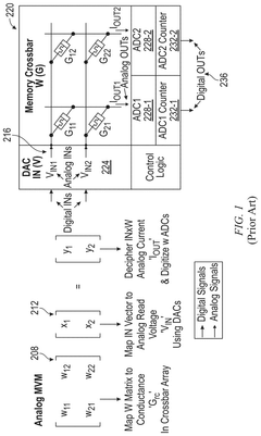
01 Analog Implementation of In-Memory Computing Accelerators
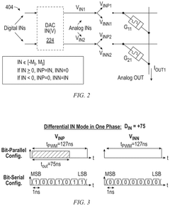
Analog implementations of in-memory computing accelerators leverage continuous signal processing to perform computations directly within memory arrays. These designs typically offer higher energy efficiency and computational density compared to digital approaches, making them suitable for neural network applications. Analog implementations often utilize resistive memory elements like memristors or phase-change memory to store weights and perform matrix multiplications through physical processes such as Ohm's law and Kirchhoff's current law.- Analog Implementation of In-Memory Computing Accelerators: Analog implementations of in-memory computing accelerators leverage continuous signal processing to perform computations directly within memory arrays. These designs typically use resistive or capacitive elements to represent weights and perform matrix operations through physical phenomena like Ohm's law. Analog approaches offer advantages in power efficiency and computation density for neural network applications, though they face challenges with precision and noise sensitivity.
- Digital Implementation of In-Memory Computing Accelerators: Digital in-memory computing accelerators perform discrete computations using binary logic directly within or near memory arrays. These implementations typically use SRAM, DRAM, or emerging memory technologies with integrated digital processing elements. Digital approaches provide benefits in accuracy, programmability, and compatibility with existing digital systems, though they may consume more power and area compared to analog counterparts for certain workloads.
- Hybrid Analog-Digital Architectures: Hybrid architectures combine both analog and digital processing elements to leverage the advantages of each approach. These systems typically use analog computation for the most computationally intensive operations while employing digital circuits for control, precision enhancement, and post-processing. This approach aims to balance the energy efficiency of analog computing with the precision and flexibility of digital systems, particularly for neural network inference applications.
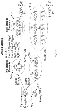
- Memory Technology Selection for In-Memory Computing: The choice of memory technology significantly impacts in-memory computing accelerator performance. Emerging non-volatile memories like resistive RAM, phase-change memory, and magnetoresistive RAM offer advantages for analog computing due to their inherent ability to store multiple states and perform operations in place. Traditional SRAM and DRAM can be modified for digital in-memory computing by adding computational elements within memory arrays or in close proximity to reduce data movement.
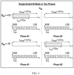
- Signal Processing and Data Conversion Techniques: Signal processing and data conversion techniques are crucial for in-memory computing accelerators, particularly at the interface between analog and digital domains. These include specialized analog-to-digital converters, digital-to-analog converters, and signal conditioning circuits that address challenges like noise, non-linearity, and process variations. Advanced techniques such as stochastic computing and approximate computing can be employed to optimize the performance-accuracy tradeoff in these systems.
02 Digital Implementation of In-Memory Computing Accelerators
Digital in-memory computing accelerators implement computational functions using discrete binary logic directly within or near memory arrays. These implementations offer higher precision, better noise immunity, and compatibility with existing digital design flows compared to analog approaches. Digital in-memory computing typically employs SRAM or embedded DRAM with integrated logic to perform operations like bitwise computations, addition, and multiplication without transferring data to a separate processing unit.Expand Specific Solutions03 Hybrid Analog-Digital Architectures
Hybrid architectures combine analog and digital processing elements to leverage the advantages of both approaches. These implementations typically use analog computing for the core matrix operations where efficiency is paramount, while employing digital circuits for control logic, data conversion, and post-processing to ensure accuracy and programmability. Hybrid designs often incorporate ADCs and DACs at strategic points in the processing pipeline to manage the interface between analog and digital domains.Expand Specific Solutions04 Memory Technology Selection for In-Memory Computing
The choice of memory technology significantly impacts the implementation approach for in-memory computing accelerators. Various memory technologies including SRAM, DRAM, flash, resistive RAM (RRAM), phase-change memory (PCM), and magnetic RAM (MRAM) offer different trade-offs in terms of density, speed, power consumption, and compatibility with computational functions. The selection depends on application requirements, with emerging non-volatile memories enabling new capabilities for persistent in-memory computing.Expand Specific Solutions05 Application-Specific Optimization Techniques
In-memory computing accelerators can be optimized for specific applications through specialized circuit designs and algorithmic approaches. These optimizations include precision scaling, sparsity exploitation, and workload-specific memory hierarchies. For machine learning applications, techniques such as weight pruning, quantization, and efficient mapping of neural network layers to memory arrays can significantly improve performance and energy efficiency. Custom data flow architectures tailored to application characteristics further enhance the effectiveness of in-memory computing solutions.Expand Specific Solutions
Key Industry Players in IMC Accelerator Development
In-memory computing accelerators are evolving rapidly, with the market currently in a growth phase characterized by increasing adoption across AI and edge computing applications. The technology landscape shows a competitive divide between analog and digital implementations, each offering distinct advantages in performance-power tradeoffs. Major semiconductor players like IBM, Intel, and Qualcomm are advancing digital approaches with established manufacturing processes, while startups like Encharge AI pursue innovative analog solutions offering potentially higher energy efficiency. Academic institutions including Peking University and USC are contributing fundamental research, particularly in analog implementations. Memory manufacturers Micron and TSMC are strategically positioned to integrate computing capabilities directly into memory architectures. The market is expected to expand significantly as applications in edge AI, IoT, and data centers drive demand for more efficient computing solutions.
International Business Machines Corp.
Technical Solution: IBM在存内计算领域采用混合模拟-数字方法,开发了基于相变存储器(PCM)的存内计算架构。其技术方案结合了模拟计算的能效优势和数字计算的精确性,通过在PCM阵列中直接执行矩阵乘法运算,显著减少了数据移动。IBM的存内计算加速器在8位精度下实现了比传统GPU高出200倍的能效比[1]。该技术利用PCM单元的模拟特性存储权重,同时采用数字接口进行精确控制和读取,形成了独特的混合架构。IBM还开发了专门的编译器和软件栈,使深度学习框架能够无缝利用这种新型计算范式,特别适用于边缘AI应用场景[2]。
优势:能效比极高,在低功耗场景下表现卓越;PCM技术成熟度高;软件生态系统完善。劣势:在高精度计算场景下性能受限;模拟部分容易受到环境因素如温度波动的影响;与纯数字实现相比,系统复杂度更高,可能增加制造和维护成本。
Intel Corp.
Technical Solution: Intel的存内计算技术方案主要围绕其Optane技术和3D XPoint存储器展开,采用数字优先的混合实现方式。Intel开发了专用的存内计算处理单元(IMPU),将其集成到存储控制器中,实现了数据就近处理。其架构保持了数字计算的高精度特性,同时通过减少数据移动提升能效。Intel的方案特别注重与现有x86架构的兼容性,开发了扩展指令集使常规CPU能够高效调用存内计算功能[3]。在大规模数据分析应用中,Intel的存内计算加速器展示了高达15倍的性能提升和8倍的能效改善[4]。该技术还特别优化了对稀疏矩阵运算的支持,这在许多AI和科学计算应用中至关重要。
优势:与现有x86生态系统高度兼容;数字实现保证了计算精度;在大规模数据分析场景表现出色。劣势:相比纯模拟实现,能效提升空间有限;Optane技术商业化进展受阻;在极低功耗场景下不如模拟实现方案高效。
Core Patents and Technical Innovations in IMC
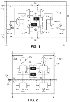
In-memory matrix multiplication with binary complement inputs
PatentPendingUS20250245286A1
Innovation
- Implement a matrix-vector multiplication device using binary complement inputs, a crossbar array with differential analog conductance, and a digital COMP counter to perform matrix-vector multiplication, eliminating the need for duplicate weights, differential ADCs, and P/N counters, and reducing the complexity of ADCs.
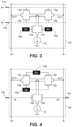
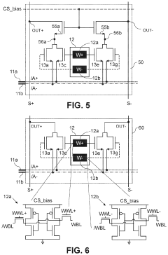
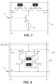
Analog in-memory computing based inference accelerator
PatentActiveUS11699482B2
Innovation
- The implementation of a compute cell with a memory unit storing ternary weights and a logic unit that selectively enables conductive paths for charging and discharging read bit lines based on the signs of the weights and input data, allowing for more dense storage and wider multiplication operations, thereby enhancing energy efficiency and reducing variations across compute cells.
Power Efficiency Comparison Between Analog and Digital IMC
Power efficiency represents a critical differentiator between analog and digital implementations of In-Memory Computing (IMC) accelerators. Analog IMC designs typically demonstrate superior power efficiency for specific workloads, particularly in neural network inference tasks. This advantage stems from their ability to perform multiply-accumulate operations directly within memory arrays using physical properties such as Ohm's law and Kirchhoff's current law, eliminating the need for data movement between separate processing and memory units.
Quantitative comparisons reveal that analog IMC implementations can achieve energy efficiencies of 10-100 TOPS/W (Tera Operations Per Second per Watt), significantly outperforming digital counterparts that typically deliver 1-10 TOPS/W for similar computational tasks. This order-of-magnitude improvement derives from the fundamental reduction in data movement energy costs, which can account for up to 90% of total system energy in conventional von Neumann architectures.
However, analog IMC's power efficiency advantages come with important caveats. The power efficiency of analog designs deteriorates significantly when high precision computation is required, as analog-to-digital and digital-to-analog conversion circuits consume substantial power at higher bit precisions. For applications requiring 8-bit or higher precision, the power efficiency gap between analog and digital implementations narrows considerably.
Digital IMC implementations, while generally less power-efficient for low-precision operations, offer more consistent performance across varying computational precision requirements. They maintain reasonable efficiency even as precision increases, making them more versatile for applications with dynamic precision needs. Additionally, digital designs benefit from established power management techniques such as dynamic voltage and frequency scaling, which are less straightforward to implement in analog systems.
Environmental factors also influence the power efficiency equation. Analog IMC implementations exhibit greater sensitivity to temperature variations, potentially requiring additional power for thermal management in deployment scenarios with unstable thermal conditions. This sensitivity can erode their theoretical power efficiency advantages in practical applications.
Recent hybrid approaches combining analog computation with digital control and conversion have emerged as promising solutions that balance the power efficiency benefits of analog computation with the precision and stability advantages of digital systems. These designs strategically allocate computational tasks between analog and digital domains to optimize overall system power efficiency while maintaining acceptable computational accuracy.
Fabrication and Integration Challenges for IMC Technologies
The fabrication and integration of In-Memory Computing (IMC) technologies present significant challenges that differ substantially between analog and digital implementations. Analog IMC devices, while offering higher computational density and energy efficiency, face considerable manufacturing hurdles related to process variations and device non-idealities. These variations can significantly impact computational accuracy and reliability, requiring sophisticated compensation techniques during fabrication.
Digital IMC implementations, conversely, benefit from established CMOS manufacturing processes but encounter challenges in achieving the same level of parallelism and energy efficiency as their analog counterparts. The integration of memory arrays with computational elements demands careful consideration of signal integrity, thermal management, and power distribution networks.
For emerging non-volatile memory (NVM) technologies used in IMC, such as RRAM, PCM, and MRAM, specialized fabrication processes must be developed to ensure compatibility with standard CMOS processes. This co-integration often requires additional masking steps and thermal budget management, increasing manufacturing complexity and cost. The back-end-of-line (BEOL) integration of these novel materials introduces challenges in maintaining the integrity of existing structures while accommodating new process requirements.
Scaling presents another critical challenge, particularly for analog IMC implementations. As device dimensions shrink, quantum effects and increased variability can compromise computational precision. Digital implementations face less severe scaling issues but must contend with increased interconnect delays and power density concerns at advanced nodes.
3D integration approaches offer promising solutions to overcome some fabrication challenges by enabling higher memory density and reduced interconnect lengths. However, these approaches introduce new complexities related to through-silicon vias (TSVs), thermal management, and yield optimization. Monolithic 3D integration, while theoretically advantageous for IMC architectures, remains challenging due to process temperature constraints and alignment precision requirements.
Testing and validation methodologies for IMC technologies require significant adaptation from conventional memory testing approaches. Analog IMC implementations particularly necessitate new test paradigms to verify computational accuracy across various operating conditions and throughout device lifetime. This includes characterization of device-to-device variations and development of appropriate redundancy schemes to maintain system-level reliability.
Ultimately, the choice between analog and digital IMC implementations involves careful consideration of these fabrication and integration challenges against application requirements for computational precision, energy efficiency, and system reliability.
Unlock deeper insights with Patsnap Eureka Quick Research — get a full tech report to explore trends and direct your research. Try now!
Generate Your Research Report Instantly with AI Agent
Supercharge your innovation with Patsnap Eureka AI Agent Platform!