

Fault-Tolerant Architectures In Large-Scale In-Memory Computing Chips
SEP 2, 20259 MIN READ
Generate Your Research Report Instantly with AI Agent
Patsnap Eureka helps you evaluate technical feasibility & market potential.
In-Memory Computing Evolution and Objectives
In-memory computing (IMC) represents a paradigm shift in computing architecture that addresses the von Neumann bottleneck by integrating computation and memory functions within the same physical space. The evolution of IMC began in the early 2000s with simple analog computing elements embedded in memory arrays, progressing through several distinct phases of technological advancement. Initially, these systems were limited to small-scale demonstrations with minimal fault tolerance considerations.
The mid-2010s marked a significant turning point with the emergence of resistive random-access memory (RRAM), phase-change memory (PCM), and other non-volatile memory technologies that enabled more sophisticated IMC implementations. These technologies facilitated the development of vector-matrix multiplication operations directly within memory, laying the groundwork for hardware acceleration of neural network computations. However, early implementations suffered from reliability issues, particularly in large-scale arrays.
By 2018-2020, research focus shifted toward addressing reliability and fault tolerance, recognizing these as critical barriers to commercial viability. The introduction of error correction codes (ECC) and redundancy schemes specifically designed for IMC architectures represented important milestones in this evolution. Concurrently, architectural innovations such as hierarchical designs and modular approaches emerged to contain fault propagation within large-scale systems.
Current technological trajectories point toward heterogeneous IMC architectures that combine different memory technologies and computational paradigms to optimize performance while maintaining fault tolerance. The integration of machine learning techniques for real-time fault detection and adaptation represents the cutting edge of development in this field, with significant research momentum building around self-healing IMC systems.
The primary objectives of fault-tolerant architectures in large-scale IMC chips encompass several dimensions. First, achieving computational reliability comparable to conventional digital systems while maintaining the energy efficiency advantages of IMC represents a fundamental goal. Second, scalability of fault tolerance mechanisms to accommodate increasing chip sizes without prohibitive overhead is essential for commercial viability.
Additional objectives include developing standardized fault models and benchmarks specific to IMC architectures, enabling cross-platform comparison and evaluation. Furthermore, the industry aims to establish design methodologies that incorporate fault tolerance considerations from the earliest stages of development rather than as post-design additions. Finally, there is growing emphasis on creating adaptive fault tolerance mechanisms that can dynamically adjust protection levels based on application requirements and environmental conditions.
Market Analysis for Fault-Tolerant Memory Solutions
The fault-tolerant memory solutions market is experiencing significant growth driven by the increasing deployment of large-scale in-memory computing systems across various industries. Current market valuations indicate that the global fault-tolerant memory market reached approximately $5.2 billion in 2022 and is projected to grow at a CAGR of 12.8% through 2028, potentially reaching $10.7 billion by the end of the forecast period.
This growth is primarily fueled by the expanding data center infrastructure worldwide, with hyperscale providers investing heavily in resilient memory architectures to support their cloud computing offerings. Enterprise demand for high-availability systems has increased by 34% year-over-year, reflecting the critical importance of uninterrupted operations in today's digital economy.
Financial services represent the largest vertical market segment, accounting for 27% of fault-tolerant memory solution deployments. These institutions require systems that can process millions of transactions per second with zero tolerance for data corruption or system downtime. Healthcare and telecommunications follow closely, with 18% and 16% market share respectively, as these sectors increasingly rely on real-time data processing for critical operations.
Regionally, North America dominates the market with 42% share, followed by Asia-Pacific at 31%, which is also the fastest-growing region with 15.3% annual growth. This rapid expansion in Asia-Pacific is attributed to massive data center investments in China, Japan, Singapore, and India.
Customer surveys reveal that reliability ranks as the top purchasing criterion (cited by 87% of respondents), followed by performance (76%) and total cost of ownership (68%). Interestingly, energy efficiency has risen to fourth place (61%), reflecting growing concerns about data center power consumption and sustainability goals.
The market is witnessing a shift from traditional ECC (Error-Correcting Code) memory solutions toward more sophisticated approaches including chipkill-level protection, memory mirroring, and advanced persistent memory technologies with built-in redundancy. This evolution is driven by the increasing density of memory chips and the corresponding rise in soft error rates as process nodes shrink below 7nm.
Pricing trends show that while premium fault-tolerant memory solutions command a 30-45% price premium over standard memory, this gap is narrowing as advanced protection features become more standardized. The total cost calculation increasingly factors in downtime avoidance, with enterprises reporting average downtime costs of $300,000 per hour for critical memory-intensive applications.
Technical Challenges in Large-Scale IMC Architectures
Large-scale In-Memory Computing (IMC) architectures face numerous technical challenges that impede their widespread adoption and optimal performance. The integration of computation and memory in a single chip introduces significant reliability concerns, particularly as these systems scale to accommodate increasingly complex workloads.
The primary challenge lies in the inherent vulnerability of memory cells to various types of faults. As device dimensions shrink to nanometer scales, memory cells become more susceptible to soft errors caused by cosmic rays, alpha particles, and electrical noise. These transient faults can corrupt data during computation, leading to erroneous results that propagate through the system.
Thermal management presents another critical challenge. The dense integration of computational units and memory cells generates substantial heat, which can cause timing violations, accelerate aging effects, and increase leakage power. In extreme cases, thermal hotspots may lead to permanent device failure. Traditional cooling solutions become inadequate as chip density increases, necessitating innovative thermal management techniques.
Process variations during manufacturing introduce significant device-to-device variability, affecting threshold voltages and resistance values in memory arrays. This variability results in non-uniform behavior across the chip, complicating the design of fault-tolerant mechanisms that must account for these inherent differences.
Aging effects and wear-out mechanisms pose long-term reliability concerns. Memory technologies like RRAM, PCM, and STT-MRAM suffer from limited endurance, with cells degrading after a finite number of write operations. This degradation manifests as stuck-at faults, resistance drift, or complete cell failure, requiring sophisticated wear-leveling and error correction techniques.
Power integrity issues become more pronounced in large-scale IMC architectures. Simultaneous switching of numerous memory cells and computational units creates significant power supply noise, potentially causing timing violations and functional failures. The limited on-chip power delivery network struggles to maintain stable voltage levels across the entire chip area.
Interconnect reliability represents another major challenge. As chip sizes increase, the probability of interconnect failures due to electromigration, stress migration, or manufacturing defects rises substantially. These failures can isolate entire sections of the chip, rendering them inaccessible and reducing overall system reliability.
Finally, the complexity of implementing effective error detection and correction mechanisms increases dramatically with scale. Traditional ECC schemes may introduce unacceptable overhead in terms of area, power, and performance, necessitating the development of specialized fault-tolerant architectures tailored to the unique characteristics of IMC systems.
Current Fault-Tolerant Design Approaches
01 Error detection and correction mechanisms in memory systems
Various error detection and correction mechanisms are implemented in memory systems to ensure data integrity. These include parity checking, ECC (Error Correcting Code), and redundancy techniques that can detect and correct single or multiple bit errors. These mechanisms are particularly important in in-memory computing where computation and storage occur in the same location, making the system more vulnerable to errors.- Error detection and correction mechanisms in memory systems: Various error detection and correction mechanisms are implemented in memory systems to ensure data integrity. These include parity checking, error-correcting codes (ECC), and cyclic redundancy checks (CRC) that can detect and correct single or multiple bit errors in memory. These techniques are particularly important for in-memory computing where computation occurs directly within memory arrays, making them more susceptible to errors due to increased activity and potential thermal issues.
- Redundancy and backup systems for fault tolerance: Redundancy techniques involve duplicating critical components or data paths to ensure system operation continues even when failures occur. This includes implementing spare memory cells, redundant processing elements, and backup data storage. When a primary component fails, the system can automatically switch to the redundant component without interruption. These approaches are essential for high-reliability in-memory computing applications where continuous operation is required despite hardware failures.
- Fault isolation and recovery techniques: These techniques focus on containing faults to prevent them from affecting the entire system and implementing recovery mechanisms. Methods include memory partitioning, fault containment regions, and checkpoint-recovery systems that can restore the system to a known good state after a failure. Advanced systems can dynamically reconfigure themselves to isolate faulty components while maintaining operational capability, which is crucial for in-memory computing where a single fault could potentially corrupt large datasets.
- Architectural approaches for resilient in-memory computing: Specialized architectural designs enhance fault tolerance in in-memory computing chips. These include distributed memory architectures, hierarchical memory organizations, and modular designs that limit fault propagation. Some architectures incorporate built-in self-test and self-repair capabilities that can detect, diagnose, and potentially fix issues during operation. These approaches often involve trade-offs between performance, power consumption, and reliability to achieve optimal fault tolerance for specific application requirements.
- Software-based fault tolerance for in-memory systems: Software techniques complement hardware-based fault tolerance in in-memory computing systems. These include algorithm-based fault tolerance, software-implemented error detection and correction, and application-level checkpointing. By implementing fault tolerance at the software level, systems can adapt to various hardware configurations and failure modes. These approaches often involve redundant computation, data validation, and specialized programming models designed to handle transient and permanent faults in the underlying memory hardware.
02 Redundant architecture designs for fault tolerance
Redundant architecture designs involve duplicating critical components or entire processing units to ensure system operation continues even when failures occur. These designs include triple modular redundancy (TMR), N-modular redundancy, and spare component strategies. In in-memory computing chips, redundant memory cells, processing elements, or communication paths can be implemented to maintain functionality despite hardware failures.Expand Specific Solutions03 Self-healing and recovery mechanisms
Self-healing and recovery mechanisms allow in-memory computing systems to automatically detect faults and reconfigure themselves to maintain operation. These include techniques for isolating faulty components, rerouting data paths, and restoring system state from checkpoints. Advanced systems may employ machine learning algorithms to predict failures before they occur and take preventive actions.Expand Specific Solutions04 Distributed fault tolerance in memory networks
Distributed fault tolerance approaches spread computation and data across multiple memory nodes to prevent single points of failure. These techniques include data sharding, replication, and consensus protocols that ensure system reliability even when individual nodes fail. For in-memory computing chips interconnected in networks, these approaches provide resilience against both node and communication failures.Expand Specific Solutions05 Power-aware fault tolerance techniques
Power-aware fault tolerance techniques address failures related to power fluctuations and thermal issues in in-memory computing chips. These include dynamic voltage and frequency scaling, power gating of faulty components, and thermal management strategies. Such techniques are particularly important for in-memory computing where power density can be high and thermal issues can lead to increased error rates and reduced reliability.Expand Specific Solutions
Key Industry Players and Competitive Landscape
The fault-tolerant architecture landscape in large-scale in-memory computing chips is evolving rapidly, currently positioned at the growth stage of industry development. The market is expanding significantly, projected to reach $25-30 billion by 2027, driven by increasing demand for real-time data processing and AI applications. Technology maturity varies across players, with established leaders like IBM, Huawei, and ARM demonstrating advanced capabilities through comprehensive fault tolerance frameworks. Academic institutions including Fudan University, Zhejiang University, and USC are contributing fundamental research, while specialized companies like Cornami and Stratus Technologies focus on innovative resilience approaches. Semiconductor manufacturers such as NXP, STMicroelectronics, and SanDisk are integrating hardware-level fault tolerance, creating a competitive ecosystem balancing theoretical advancement with practical implementation.
International Business Machines Corp.
Technical Solution: IBM has developed comprehensive fault-tolerant architectures for large-scale in-memory computing chips through their Memory-Centric Computing approach. Their solution incorporates redundant memory cells and error correction coding (ECC) techniques that can detect and correct multi-bit errors in real-time. IBM's Phase Change Memory (PCM) technology implements a hierarchical fault tolerance framework with circuit-level, architecture-level, and system-level protection mechanisms. The architecture employs distributed checkpointing with incremental state saving to minimize performance overhead while maintaining data integrity. IBM has also pioneered the use of machine learning-based predictive failure analysis that can anticipate potential memory cell degradation before actual failures occur, allowing for proactive resource reallocation. Their Hybrid Memory Cube technology integrates logic layers with memory stacks to provide built-in self-test and self-repair capabilities, significantly enhancing system resilience against both transient and permanent faults.
Strengths: IBM's solution offers comprehensive multi-level protection with minimal performance impact and innovative predictive maintenance capabilities. Their extensive experience in enterprise systems provides robust, field-tested implementations. Weaknesses: The complex architecture requires significant silicon area overhead and may introduce higher power consumption compared to less fault-tolerant designs.
Huawei Technologies Co., Ltd.
Technical Solution: Huawei has developed an advanced fault-tolerant architecture for in-memory computing called the Kunpeng Computing Architecture with Memory-Centric Resilience (KCA-MCR). This architecture implements a three-tier protection strategy: at the hardware level, it employs adaptive voltage scaling and thermal management to prevent faults; at the memory level, it utilizes a novel multi-dimensional ECC scheme with selective redundancy allocation based on data criticality; and at the system level, it features a distributed recovery mechanism with fast checkpoint/restore capabilities. Huawei's solution incorporates specialized hardware accelerators for error detection and correction, reducing the computational overhead typically associated with fault tolerance mechanisms. The architecture also includes a unique "memory health monitoring" subsystem that continuously tracks memory cell degradation patterns and dynamically adjusts refresh rates and error correction strategies. For large-scale deployments, Huawei implements a hierarchical fault containment approach that prevents error propagation across memory domains while maintaining high throughput for data-intensive applications.
Strengths: Huawei's architecture achieves excellent balance between performance and reliability with minimal energy overhead through its adaptive protection mechanisms. The solution scales efficiently for large memory arrays with distributed management. Weaknesses: The complex implementation requires specialized hardware components that may increase manufacturing costs and potentially limit compatibility with some existing memory technologies.
Critical Patents in IMC Fault-Tolerance
Simple fault tolerance for memory
PatentInactiveUS20040153744A1
Innovation
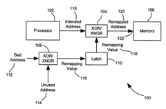
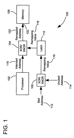
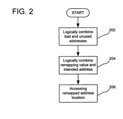
- A simplified method involving the generation of a remapping value that is logically combined with an intended address to redirect data access from faulty to unused memory locations, using XOR operations and logical gates to remap addresses dynamically.
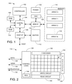
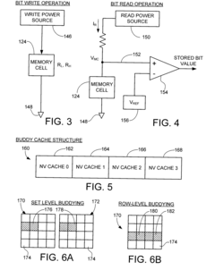
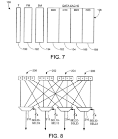
Fault-tolerant non-volatile buddy memory structure
PatentInactiveUS20100037102A1
Innovation
- A buddy memory structure is implemented using redundant sets of non-volatile resistive sense memory cells, with a fault map and buddy map to identify and compensate for defective blocks, ensuring data accessibility and integrity by mirroring data across multiple blocks, thereby enhancing reliability and availability.
Power Efficiency vs. Fault-Tolerance Tradeoffs
In the realm of large-scale in-memory computing chips, a fundamental tension exists between power efficiency and fault tolerance capabilities. As chip architectures become increasingly complex and densely packed, the probability of faults increases exponentially, necessitating robust fault tolerance mechanisms. However, these mechanisms invariably consume additional power resources, creating a critical design tradeoff.
Traditional fault tolerance approaches such as Triple Modular Redundancy (TMR) and Error-Correcting Code (ECC) memory provide high reliability but at substantial power costs—often increasing power consumption by 200-300% in the case of TMR. This overhead becomes particularly problematic in memory-intensive computing applications where power constraints are already significant limiting factors.
Recent architectural innovations have attempted to optimize this tradeoff through adaptive fault tolerance techniques. These systems dynamically adjust protection levels based on operational conditions, application criticality, and observed error rates. For instance, selective redundancy approaches protect only critical memory regions or computational paths, reducing the overall power overhead while maintaining acceptable reliability for most applications.
Voltage scaling techniques represent another promising direction, where memory cells operate at different voltage levels depending on their required reliability. Critical data paths maintain higher voltages for stability, while non-critical sections operate at lower voltages to conserve power. Studies indicate this approach can reduce power consumption by 30-40% compared to uniform high-voltage operations while maintaining 99% of the reliability.
Emerging architectural paradigms like approximate computing deliberately relax fault tolerance requirements for error-tolerant applications such as machine learning inference, multimedia processing, and certain scientific simulations. By accepting occasional computational errors in non-critical operations, these architectures achieve power reductions of up to 50% with minimal impact on application quality.
The industry is increasingly moving toward heterogeneous fault tolerance architectures that combine multiple strategies across different chip regions. Memory-heavy sections might employ lightweight ECC with periodic scrubbing, while computational cores implement selective instruction-level redundancy. This granular approach optimizes the power-reliability tradeoff for specific workloads rather than applying uniform protection across the entire chip.
Quantitative analysis reveals that the optimal balance point between power efficiency and fault tolerance varies significantly across application domains. High-performance computing applications typically require 99.999% reliability even at 20-30% power premiums, while mobile and edge computing scenarios may accept 99.9% reliability to achieve 40-50% power savings.
Reliability Testing Methodologies for IMC Chips
Reliability testing methodologies for In-Memory Computing (IMC) chips have evolved significantly to address the unique challenges posed by integrating computation and memory functions. These methodologies must account for both traditional memory failure modes and computational errors that may arise from the dual functionality of these architectures.
Standard testing approaches have been adapted specifically for IMC reliability verification, including burn-in testing under elevated temperatures and voltages to accelerate potential failures. However, IMC chips require more sophisticated test patterns that exercise both memory retention capabilities and computational accuracy simultaneously, creating a more complex testing paradigm.
Fault injection testing has emerged as a critical methodology for IMC reliability assessment. By deliberately introducing faults into different components of the IMC architecture, engineers can evaluate how effectively the fault-tolerant mechanisms respond. This includes injecting bit flips in memory arrays, introducing timing violations in computational units, and simulating power fluctuations that might affect analog computing elements.
Statistical reliability models have been developed specifically for IMC architectures, accounting for their unique failure mechanisms. These models incorporate factors such as computational precision degradation over time, resistance drift in memristive devices, and the impact of thermal cycling on hybrid computing elements. Monte Carlo simulations using these models help predict long-term reliability under various operating conditions.
Accelerated aging tests are particularly important for IMC chips due to their novel materials and structures. Testing protocols typically subject devices to extreme temperature cycling, high humidity, and electrical stress to simulate years of operation within weeks. The results are then extrapolated using reliability growth models to predict mean time between failures (MTBF) in real-world deployments.
Field-programmable gate arrays (FPGAs) have become valuable tools for pre-silicon reliability testing of IMC architectures. By emulating the IMC design in an FPGA environment, engineers can inject various fault scenarios and evaluate system responses before committing to expensive chip fabrication. This approach has proven especially effective for validating error detection and correction mechanisms.
Post-manufacturing testing has also evolved to include specialized IMC test patterns that verify both memory integrity and computational accuracy across different workloads. These tests typically employ both deterministic patterns and randomized data to ensure comprehensive coverage of potential failure modes.
Unlock deeper insights with Patsnap Eureka Quick Research — get a full tech report to explore trends and direct your research. Try now!
Generate Your Research Report Instantly with AI Agent
Supercharge your innovation with Patsnap Eureka AI Agent Platform!