

In-Memory Computing For Low-Latency Edge Artificial Intelligence Applications
SEP 2, 20259 MIN READ
Generate Your Research Report Instantly with AI Agent
PatSnap Eureka helps you evaluate technical feasibility & market potential.
In-Memory Computing Background and Objectives
In-memory computing represents a paradigm shift in computer architecture that addresses the fundamental bottleneck in traditional von Neumann architectures: the separation between processing and memory units. This separation creates significant data transfer latency, commonly referred to as the "memory wall," which has become increasingly problematic as computational demands grow, particularly for data-intensive applications like artificial intelligence.
The evolution of in-memory computing can be traced back to the early concepts of content-addressable memory in the 1960s, followed by associative processing in subsequent decades. However, it wasn't until recent advancements in non-volatile memory technologies and the pressing demands of edge AI applications that in-memory computing gained significant momentum as a viable solution for low-latency processing.
Edge AI applications present unique challenges that traditional computing architectures struggle to address efficiently. These applications require real-time processing of sensor data, image recognition, natural language processing, and other AI workloads directly on edge devices with strict power, size, and latency constraints. The conventional approach of transferring data between memory and processing units becomes prohibitively expensive in terms of energy consumption and processing time.
The primary objective of in-memory computing research for edge AI is to develop architectures that can perform computations directly within memory arrays, eliminating or significantly reducing data movement. This approach aims to achieve orders of magnitude improvements in energy efficiency and processing speed for AI workloads at the edge.
Current research trajectories focus on several promising technologies, including resistive random-access memory (RRAM), phase-change memory (PCM), ferroelectric RAM (FeRAM), and magnetoresistive RAM (MRAM). These emerging memory technologies offer the dual capability of data storage and computation, making them ideal candidates for in-memory computing implementations.
The technical goals of in-memory computing research encompass developing scalable architectures that can efficiently execute neural network operations such as matrix multiplication and convolution directly within memory arrays. Additionally, researchers aim to create programming models and compilation tools that abstract the complexity of in-memory computing, enabling software developers to leverage these architectures without specialized knowledge of the underlying hardware.
As edge AI applications continue to proliferate across industries including healthcare, autonomous vehicles, smart cities, and industrial IoT, the demand for low-latency, energy-efficient computing solutions grows exponentially. In-memory computing stands at the forefront of technologies poised to meet these demands, potentially revolutionizing how AI computations are performed at the edge.
Market Analysis for Low-Latency Edge AI Solutions
The edge AI market is experiencing explosive growth, driven by the increasing demand for real-time processing capabilities in IoT devices, autonomous vehicles, smart cities, and industrial automation. According to market research, the global edge AI hardware market is projected to reach $38.9 billion by 2030, with a compound annual growth rate (CAGR) of 18.8% from 2023 to 2030. This remarkable growth trajectory underscores the critical importance of low-latency solutions in edge computing environments.
The demand for in-memory computing solutions specifically tailored for edge AI applications stems from several key market factors. First, there is a growing need for real-time decision-making capabilities in mission-critical applications such as autonomous driving, industrial safety systems, and medical devices. These applications cannot tolerate the latency associated with cloud-based processing and require immediate local computation.
Second, privacy concerns and regulatory requirements are pushing computation to the edge, where sensitive data can be processed without transmission to centralized servers. This trend is particularly evident in regions with strict data protection regulations like Europe (GDPR) and California (CCPA).
Third, bandwidth limitations and connectivity issues in remote or mobile environments necessitate edge processing capabilities that can function reliably without constant cloud connectivity. This is especially relevant for applications in rural areas, developing regions, or mobile platforms where network infrastructure may be limited or unreliable.
Market segmentation reveals that the automotive sector represents the largest vertical market for low-latency edge AI solutions, accounting for approximately 24% of the total market share. This is followed by industrial automation (19%), consumer electronics (17%), healthcare (14%), and smart cities (12%), with various other applications comprising the remaining 14%.
From a geographical perspective, North America currently leads the market with a 38% share, followed by Asia-Pacific at 34%, Europe at 21%, and the rest of the world at 7%. However, the Asia-Pacific region is expected to witness the fastest growth rate over the next five years due to rapid industrialization, smart city initiatives, and significant investments in AI infrastructure by countries like China, Japan, and South Korea.
The market for in-memory computing solutions specifically designed for edge AI applications is currently dominated by established semiconductor companies and specialized AI hardware startups. These companies are competing to develop more efficient architectures that can deliver higher performance per watt, a critical metric for edge deployment where power constraints are often significant.
In-Memory Computing Status and Technical Barriers
In-memory computing (IMC) represents a paradigm shift in computing architecture, addressing the von Neumann bottleneck by integrating computation and memory functions. Currently, IMC technologies have reached varying levels of maturity across different implementation approaches. Resistive random-access memory (RRAM) and phase-change memory (PCM) based solutions have demonstrated promising results in research environments, with several prototypes achieving energy efficiencies of 10-100 TOPS/W for AI inference tasks. However, commercial deployment remains limited primarily to specialized applications.
The global landscape shows concentrated research efforts in the United States, China, and Europe. Major research institutions like Stanford, MIT, and Tsinghua University have established dedicated IMC research centers, while industry leaders including IBM, Intel, and Samsung have invested significantly in IMC technology development. Recent advancements include analog crossbar arrays achieving up to 1000x improvement in energy efficiency for matrix multiplication operations compared to conventional GPU implementations.
Despite progress, several critical technical barriers impede widespread adoption of IMC for edge AI applications. Device variability presents a fundamental challenge, with resistance fluctuations in memristive devices causing computational inaccuracies that compromise AI model performance. Current manufacturing processes struggle to maintain consistent device characteristics across large arrays, resulting in reduced computational precision.
Scaling limitations constitute another significant barrier. As device dimensions shrink below 20nm, quantum effects and thermal instabilities introduce unpredictable behaviors that affect reliability. Additionally, the non-linear I-V characteristics of many memristive devices complicate the implementation of precise analog computing operations required for neural network processing.
Limited endurance represents a persistent challenge, with many IMC devices exhibiting degradation after 10^6-10^9 programming cycles—insufficient for dynamic AI workloads requiring frequent weight updates. This constraint particularly affects online learning applications at the edge.
The lack of standardized design tools and methodologies further hinders development. Current electronic design automation (EDA) tools are not optimized for IMC architectures, creating significant barriers for system designers attempting to implement IMC solutions. The absence of unified programming models and frameworks also complicates software development for these novel architectures.
Integration challenges with conventional CMOS technology present additional hurdles. Interfacing analog IMC cores with digital peripherals introduces signal conversion overhead that can negate performance gains, while thermal management issues in densely packed IMC arrays can lead to reliability concerns in edge devices with limited cooling capabilities.
Current In-Memory Computing Architectures for Edge AI
01 Memory architecture optimization for reduced latency
Optimizing memory architecture is crucial for reducing latency in in-memory computing systems. This includes designing specialized memory hierarchies, implementing efficient memory controllers, and organizing memory cells to minimize access time. These architectural improvements enable faster data retrieval and processing, significantly reducing the overall system latency for computational tasks performed directly in memory.- Memory architecture optimization for reduced latency: Optimizing memory architecture is crucial for reducing latency in in-memory computing systems. This includes designing specialized memory hierarchies, implementing efficient memory controllers, and utilizing advanced memory addressing techniques. These optimizations help minimize data access times and improve overall system performance by reducing the time required to fetch and process data within the memory subsystem.
- Data processing techniques in memory: Various data processing techniques can be implemented directly within memory to reduce computing latency. These include in-memory data compression, parallel processing capabilities, and specialized algorithms designed to operate on data without moving it to the CPU. By processing data where it resides, these techniques eliminate the traditional data movement bottleneck between memory and processing units, significantly reducing overall system latency.
- Memory cell design and operation improvements: Advancements in memory cell design and operation contribute to lower latency in in-memory computing systems. These improvements include faster switching mechanisms, reduced capacitance, and enhanced signal integrity. Novel memory cell architectures that support both storage and computational functions enable more efficient data processing with minimal latency overhead, allowing for faster execution of complex operations.
- System-level integration for latency reduction: System-level integration approaches focus on optimizing the entire computing stack to minimize latency in in-memory computing environments. This includes co-designing hardware and software components, implementing efficient cache coherence protocols, and developing specialized interconnects. These holistic approaches ensure that all system components work together seamlessly to reduce data access and processing delays across the computing platform.
- Memory-centric computing paradigms: Memory-centric computing paradigms represent a fundamental shift in system architecture where memory becomes the central component of the computing system rather than the processor. These approaches include processing-in-memory (PIM), near-data processing (NDP), and computational memory designs. By bringing computation closer to data or embedding computational capabilities directly within memory structures, these paradigms significantly reduce the data movement that traditionally contributes to system latency.
02 Data processing techniques within memory
Various data processing techniques can be implemented directly within memory to reduce the need for data movement between memory and processing units. These techniques include in-memory data manipulation, parallel processing capabilities embedded in memory arrays, and specialized algorithms designed for in-memory execution. By processing data where it resides, these approaches significantly reduce the latency associated with traditional compute architectures.Expand Specific Solutions03 Memory cell design and operation for faster access
Innovative memory cell designs and operation methods can substantially reduce access latency in in-memory computing systems. These include advanced transistor configurations, novel sensing mechanisms, and optimized read/write circuits. By improving the fundamental building blocks of memory systems, these innovations enable faster data access and manipulation, directly addressing the latency challenges in in-memory computing applications.Expand Specific Solutions04 System-level integration and communication optimization
System-level approaches focus on optimizing the integration and communication between memory and other system components to reduce overall latency. These include efficient interconnect designs, optimized memory-processor interfaces, and intelligent data routing mechanisms. By streamlining the flow of data throughout the system, these techniques minimize bottlenecks and reduce the latency experienced in in-memory computing environments.Expand Specific Solutions05 Workload-specific memory optimization techniques
Tailoring in-memory computing systems to specific workloads can significantly reduce latency for targeted applications. These techniques include specialized memory configurations for particular data types, application-specific memory access patterns, and customized caching strategies. By optimizing memory systems for the specific requirements of different workloads, these approaches minimize unnecessary operations and reduce the overall latency experienced by users.Expand Specific Solutions
Key Industry Players in In-Memory Computing
In-memory computing for low-latency edge AI applications is evolving rapidly, currently transitioning from early development to early adoption phase. The market is projected to grow significantly as edge AI demands increase, with an estimated value reaching billions by 2025. Technologically, the field shows varying maturity levels across players. Industry leaders like IBM, NVIDIA, and Qualcomm have established robust platforms, while specialized innovators such as Encharge AI and Deepx are developing cutting-edge solutions with novel architectures. Academic institutions including Columbia University, Tsinghua University, and EPFL are advancing fundamental research. Companies like MediaTek, ZTE, and Sony are integrating in-memory computing into commercial edge devices, creating a competitive landscape balanced between established tech giants and agile startups focused on power efficiency and performance optimization.
International Business Machines Corp.
Technical Solution: IBM has pioneered significant advancements in in-memory computing for edge AI applications through their Phase-Change Memory (PCM) technology. Their approach integrates computational functions directly within memory arrays, eliminating the need for data movement between separate processing and storage units. IBM's PCM-based in-memory computing architecture enables analog matrix-vector multiplication operations essential for neural network inference directly within the memory itself. This architecture has demonstrated up to 200x improvement in energy efficiency compared to conventional von Neumann architectures when executing AI workloads. IBM has also developed specialized hardware accelerators that leverage their in-memory computing technology specifically optimized for edge deployment, achieving latencies below 10ms for complex inference tasks while maintaining power consumption under 5W. Their solution incorporates adaptive precision techniques that dynamically adjust computational precision based on application requirements, further optimizing the performance-power tradeoff for edge AI applications.
Strengths: IBM's PCM technology offers exceptional energy efficiency and significantly reduced latency by eliminating the memory wall problem. Their mature fabrication processes enable reliable integration with existing semiconductor technologies. Weaknesses: The analog nature of their in-memory computing approach introduces challenges with computational accuracy and may require additional error correction mechanisms, potentially increasing system complexity.
École Polytechnique Fédérale de Lausanne
Technical Solution: EPFL has developed cutting-edge in-memory computing solutions for edge AI applications through their innovative research on ferroelectric FET (FeFET) memory technology. Their approach integrates computational capabilities directly within non-volatile memory arrays, enabling highly efficient neural network inference at the edge. EPFL's architecture implements a unique charge-based computing paradigm where multiple input activations are processed simultaneously within memory cells, dramatically reducing energy consumption associated with data movement. Their FeFET-based in-memory computing platform has demonstrated energy efficiencies exceeding 10 TOPS/W for convolutional neural network operations, representing a 50-100x improvement over conventional digital implementations. EPFL researchers have also developed specialized peripheral circuits that address precision and variability challenges inherent to analog computing, achieving near-digital accuracy while maintaining the energy benefits of in-memory computation. Their recent prototypes have achieved sub-millisecond inference latencies for complex AI tasks while operating at ultra-low power levels suitable for battery-powered edge devices. The architecture incorporates adaptive precision techniques that dynamically adjust computational resolution based on application requirements, further optimizing the energy-accuracy tradeoff for diverse edge AI scenarios.
Strengths: EPFL's FeFET-based approach offers exceptional energy efficiency combined with non-volatility, eliminating standby power consumption between computations. Their technology demonstrates excellent scalability potential for next-generation edge AI hardware. Weaknesses: The technology faces challenges with manufacturing complexity and integration with standard CMOS processes, potentially increasing production costs. Long-term reliability and endurance of FeFET devices under repeated computational operations require further validation.
Critical Patents and Research in In-Memory Computing
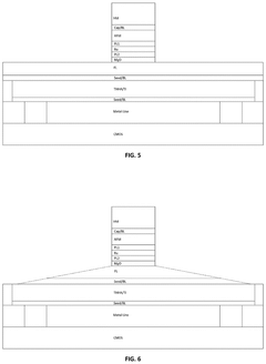
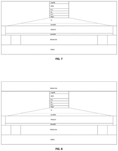
Manufacturing process to enable magntic toplogical in-memory computing ai devices
PatentPendingUS20250261564A1
Innovation
- Employing a manufacturing process that utilizes Topological Half Heusler alloy (THHA) materials and adjustable SOT-MTJ cell configurations, including adjustable free layer length and slope angle, to enhance reliability and performance of magnetic in-memory computing devices.


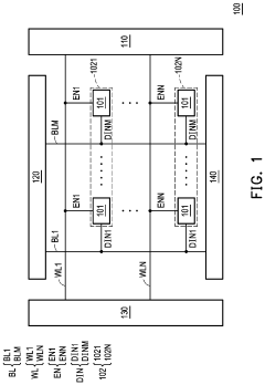
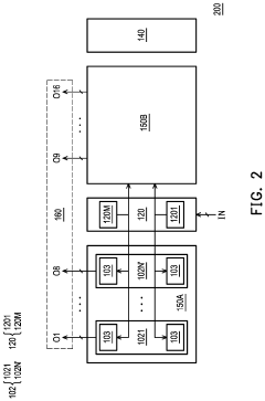
Computing-in-memory circuitry
PatentActiveUS12009054B2
Innovation
- The proposed solution involves a CIM SRAM circuit architecture that incorporates digital-to-analog converters, computing arrays, and a unified charge processing network, which improves data processing and conversion circuits to enhance energy efficiency and linearity, and includes dynamic binary-weighted current-steering digital-to-analog converters and successive-approximation analog-to-digital converters to optimize performance.
Power Efficiency Considerations for Edge Deployment
Power efficiency represents a critical constraint for in-memory computing (IMC) systems deployed at the edge. Edge devices typically operate under strict power budgets, often relying on batteries or limited power sources. The integration of IMC architectures must therefore prioritize energy optimization while maintaining the low-latency performance advantages that make them attractive for edge AI applications.
Current IMC implementations demonstrate significant power efficiency advantages compared to conventional von Neumann architectures. By eliminating the energy-intensive data movement between memory and processing units, IMC reduces overall system power consumption by 10-100x for specific AI workloads. This efficiency stems from the fundamental architectural advantage of performing computations directly within memory arrays, minimizing the energy costs associated with data transfer.
Material selection plays a crucial role in power optimization for IMC edge deployments. Emerging non-volatile memory technologies such as RRAM, PCM, and MRAM offer distinct power profiles that must be evaluated against application requirements. RRAM-based IMC solutions, for instance, demonstrate excellent static power characteristics but may require higher programming voltages. Conversely, MRAM provides faster operation with moderate power consumption but at higher manufacturing complexity.
Voltage scaling techniques represent another vital approach to power optimization in IMC systems. Recent research demonstrates that many IMC operations can function reliably at sub-nominal voltages, with some implementations showing functional operation down to 0.6V while maintaining acceptable accuracy for edge AI tasks. Adaptive voltage scaling techniques that dynamically adjust operating voltages based on workload characteristics show particular promise for edge deployments with variable computational demands.
Computational precision tuning offers additional power efficiency opportunities. Many edge AI applications can tolerate reduced numerical precision without significant accuracy degradation. IMC architectures that support variable precision operations allow for power-accuracy tradeoffs, with 8-bit and even 4-bit operations consuming substantially less energy than full-precision alternatives while maintaining acceptable inference quality for many edge applications.
Duty cycling and power gating strategies further enhance IMC power efficiency for intermittent edge computing scenarios. By selectively activating only the memory arrays required for specific operations and aggressively power-gating inactive components, modern IMC designs can achieve ultra-low standby power consumption. This approach is particularly valuable for IoT edge devices that operate primarily in monitoring modes with occasional computational bursts.
Hardware-Software Co-Design Strategies
Effective hardware-software co-design strategies are essential for maximizing the potential of in-memory computing (IMC) in edge AI applications. These strategies involve the simultaneous optimization of hardware architectures and software frameworks to achieve optimal performance, energy efficiency, and latency reduction.
At the hardware level, designers must consider the specific requirements of edge AI workloads when implementing IMC solutions. This includes optimizing memory cell designs for computational efficiency, developing specialized peripheral circuits for parallel operations, and creating efficient data movement pathways. Custom accelerators that leverage IMC principles can be tailored to specific AI tasks, such as convolutional neural networks or transformer models, further enhancing performance.
Software frameworks must evolve to effectively utilize IMC hardware capabilities. This includes developing specialized compilers that can map AI algorithms directly to IMC hardware, optimizing data flow patterns, and implementing efficient resource allocation strategies. Runtime systems need to dynamically manage workload distribution between conventional processing units and IMC components based on real-time performance requirements and energy constraints.
Memory-aware neural network design represents a critical aspect of co-design strategies. This involves adapting neural network architectures to match the characteristics of IMC hardware, such as quantization techniques optimized for specific memory cell properties, pruning methods that consider the physical layout of memory arrays, and novel training algorithms that account for the analog nature of certain IMC implementations.
Cross-layer optimization techniques bridge the gap between hardware and software domains. These include joint optimization of memory access patterns and neural network layer configurations, hardware-aware training methodologies that incorporate device characteristics into the learning process, and adaptive execution strategies that respond to changing operational conditions at the edge.
Simulation and modeling tools play a crucial role in the co-design process, allowing designers to evaluate different hardware-software configurations before physical implementation. These tools must accurately capture the unique characteristics of IMC systems, including analog computing effects, device variations, and thermal considerations.
Standardization efforts are emerging to facilitate broader adoption of IMC technologies. These include defining common interfaces between software frameworks and IMC hardware, establishing benchmarking methodologies specific to IMC-based edge AI systems, and developing reference architectures that demonstrate best practices in hardware-software co-design.
Unlock deeper insights with PatSnap Eureka Quick Research — get a full tech report to explore trends and direct your research. Try now!
Generate Your Research Report Instantly with AI Agent
Supercharge your innovation with PatSnap Eureka AI Agent Platform!