

Emerging Nanoscale Materials For Next-Generation In-Memory Computing
SEP 12, 20259 MIN READ
Generate Your Research Report Instantly with AI Agent
Patsnap Eureka helps you evaluate technical feasibility & market potential.
Nanomaterials Evolution and Research Objectives
In-memory computing has emerged as a promising paradigm to overcome the von Neumann bottleneck in conventional computing architectures. The evolution of nanomaterials for this application has undergone significant transformation over the past decades, from traditional semiconductor materials to advanced nanoscale structures with unique electrical, magnetic, and optical properties. This technological progression has been driven by the increasing demand for energy-efficient, high-performance computing systems capable of handling complex data-intensive tasks.
The field began with conventional CMOS-based memory technologies in the 1990s, which faced fundamental scaling limitations. The 2000s witnessed the emergence of first-generation non-volatile memories such as Flash, which provided improved data retention but still suffered from speed and endurance limitations. The 2010s marked a pivotal shift toward novel nanomaterials including phase-change materials, resistive switching oxides, and magnetic materials, enabling the development of emerging memory technologies like RRAM, PCM, and STT-MRAM.
Current research focuses on two-dimensional materials such as graphene, transition metal dichalcogenides (TMDs), and hexagonal boron nitride (h-BN), which offer atomic-level thickness control and unique quantum properties. These materials demonstrate exceptional carrier mobility, tunable bandgaps, and mechanical flexibility, making them ideal candidates for next-generation in-memory computing applications. Additionally, van der Waals heterostructures formed by stacking different 2D materials have shown promise for creating novel electronic devices with tailored properties.
The primary research objectives in this field include developing nanomaterials with enhanced switching characteristics, including faster switching speeds, lower energy consumption, higher endurance, and improved retention. Researchers aim to achieve multi-bit storage capabilities through precise control of intermediate resistance states, which is crucial for implementing efficient neuromorphic computing architectures. Another key goal is to enhance the scalability of these materials to enable high-density integration compatible with existing semiconductor manufacturing processes.
Furthermore, there is significant interest in exploring novel computing paradigms enabled by the unique properties of nanomaterials, such as probabilistic computing, quantum computing, and brain-inspired neuromorphic systems. These approaches could potentially overcome the fundamental limitations of conventional computing architectures and enable more efficient processing of complex data patterns, particularly for artificial intelligence applications.
The convergence of material science, device physics, and computing architecture design is essential for realizing the full potential of nanomaterials in next-generation in-memory computing. Interdisciplinary collaboration between these fields will be crucial for addressing the multifaceted challenges associated with material synthesis, device fabrication, and system integration, ultimately leading to commercially viable technologies that can revolutionize the computing landscape.
Market Analysis for In-Memory Computing Solutions
The global market for in-memory computing solutions is experiencing robust growth, driven by the increasing demand for real-time data processing and analytics across various industries. The market size was valued at approximately $3.9 billion in 2022 and is projected to reach $11.8 billion by 2028, representing a compound annual growth rate (CAGR) of 20.3% during the forecast period.
Key market drivers include the exponential growth in data generation, the rising adoption of artificial intelligence and machine learning applications, and the increasing need for faster processing capabilities in edge computing environments. Organizations across sectors are seeking solutions that can minimize data movement between storage and processing units, thereby reducing latency and energy consumption.
The financial services sector currently holds the largest market share, accounting for nearly 28% of the total market value. This dominance is attributed to the sector's heavy reliance on real-time data processing for trading algorithms, fraud detection, and risk assessment. Healthcare and telecommunications sectors follow closely, with respective market shares of 19% and 17%.
Geographically, North America leads the market with a 42% share, followed by Europe (27%) and Asia-Pacific (23%). However, the Asia-Pacific region is expected to witness the highest growth rate during the forecast period, primarily due to increasing investments in digital infrastructure and the rapid adoption of advanced computing technologies in countries like China, Japan, and South Korea.
The competitive landscape is characterized by the presence of established technology giants and emerging specialized players. Key market participants include Intel, IBM, Samsung Electronics, Micron Technology, and SK Hynix, collectively accounting for approximately 65% of the market share. These companies are actively investing in research and development to enhance their in-memory computing offerings based on emerging nanoscale materials.
Customer segments can be broadly categorized into large enterprises (68% of market revenue) and small to medium-sized enterprises (32%). Large enterprises, particularly in data-intensive industries, are the early adopters of advanced in-memory computing solutions due to their substantial IT budgets and complex computational requirements.
Market challenges include high implementation costs, concerns regarding data security and integrity, and the need for specialized expertise. Additionally, the lack of standardization across different in-memory computing architectures poses integration challenges for organizations with existing IT infrastructure.
Current Nanomaterials Landscape and Technical Barriers
The current landscape of nanomaterials for in-memory computing is characterized by diverse material systems with varying degrees of technological maturity. Resistive random-access memory (RRAM) based on metal oxides such as HfO2, Ta2O5, and TiO2 has gained significant traction due to their CMOS compatibility and scalability potential. These materials exhibit reliable resistive switching behaviors essential for memory operations, though their endurance and retention characteristics remain areas of active improvement.
Phase-change materials (PCMs), particularly chalcogenide compounds like Ge2Sb2Te5 (GST), represent another prominent category with demonstrated multi-level storage capabilities. The crystalline-to-amorphous phase transitions in these materials enable distinct resistance states, making them suitable for both memory and computing functions. However, their relatively high power consumption during the phase transition process presents a significant challenge for energy-efficient computing applications.
Emerging two-dimensional materials, including graphene, MoS2, and hexagonal boron nitride (h-BN), have shown promising electrical properties for nanoscale devices. Their atomically thin nature potentially allows for ultimate scaling limits while maintaining desirable switching characteristics. Nevertheless, large-scale fabrication techniques for these materials remain underdeveloped, limiting their immediate commercial viability.
Ferroelectric materials such as HfZrO2 and doped HfO2 have recently emerged as candidates for non-volatile memory applications due to their polarization-dependent conductivity. These materials offer advantages in terms of switching speed and energy efficiency but face challenges related to reliability and integration with existing semiconductor processes.
Several critical technical barriers currently impede the widespread adoption of nanomaterials in in-memory computing architectures. Device variability represents a fundamental challenge, with cycle-to-cycle and device-to-device variations undermining the reliability required for complex computing operations. This variability stems from stochastic material processes during switching events and non-uniform material composition at the nanoscale.
Scalability issues persist across most nanomaterial platforms, with performance degradation often observed as device dimensions shrink below certain thresholds. This scaling limitation directly impacts the potential density of computing elements achievable in practical systems. Additionally, the trade-off between retention time and switching speed presents a significant design challenge, as materials exhibiting fast switching typically demonstrate poorer data retention characteristics.
Integration with conventional CMOS technology remains problematic for many emerging nanomaterials, requiring novel fabrication approaches and potentially limiting back-end-of-line compatibility. Furthermore, the long-term reliability of these materials under repeated cycling and various environmental conditions has not been fully characterized, raising concerns about their suitability for mission-critical applications.
Contemporary Nanomaterial Architectures for Computing
01 Nanoscale material synthesis and fabrication methods
Various methods for synthesizing and fabricating nanoscale materials with enhanced performance characteristics. These include techniques for creating nanoparticles, nanocomposites, and other nanoscale structures with controlled properties. The methods focus on achieving specific material characteristics through precise fabrication processes that influence the nanoscale architecture and resulting performance.- Nanoscale material synthesis and fabrication methods: Various methods for synthesizing and fabricating nanoscale materials with enhanced performance characteristics. These include techniques for creating nanoparticles, nanocomposites, and other nanoscale structures with controlled properties. The methods focus on achieving specific material characteristics through precise fabrication processes that influence the final performance of the nanomaterials in various applications.
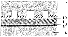
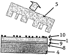
- Nanomaterial performance enhancement in polymer composites: Integration of nanomaterials into polymer matrices to create high-performance composite materials. These nanocomposites exhibit enhanced mechanical, thermal, and electrical properties compared to conventional materials. The nanoscale additives significantly improve the overall performance of the composite through various mechanisms including improved interfacial bonding, enhanced load transfer, and creation of specialized functional properties.
- Electronic and optical applications of nanomaterials: Nanomaterials designed specifically for electronic and optical applications, demonstrating superior performance in areas such as conductivity, light emission, and sensing. These materials leverage quantum effects and unique surface properties at the nanoscale to achieve functionality not possible with bulk materials. Applications include advanced semiconductors, photonic devices, sensors, and other electronic components with enhanced efficiency and performance metrics.
- Characterization and modeling of nanomaterial performance: Methods and systems for characterizing and modeling the performance of nanoscale materials. These approaches enable the prediction and measurement of nanomaterial properties and behaviors under various conditions. Advanced analytical techniques and computational models help researchers understand structure-property relationships at the nanoscale, facilitating the design of materials with targeted performance characteristics.
- Surface modification of nanomaterials for enhanced functionality: Techniques for modifying the surface properties of nanomaterials to enhance their performance in specific applications. Surface treatments and functionalization methods can improve compatibility with other materials, increase stability, and introduce new functional properties. These modifications play a crucial role in optimizing nanomaterial performance in areas such as catalysis, sensing, drug delivery, and energy storage applications.
02 Polymer-based nanomaterials and nanocomposites
Development of polymer-based nanomaterials and nanocomposites with enhanced mechanical, thermal, and electrical properties. These materials incorporate nanoscale components within polymer matrices to create materials with superior performance characteristics. The polymer nanocomposites exhibit improved strength, durability, and functionality compared to conventional materials.Expand Specific Solutions03 Carbon-based nanomaterials performance
Carbon-based nanomaterials including carbon nanotubes, graphene, and fullerenes with exceptional mechanical, electrical, and thermal properties. These materials demonstrate remarkable strength-to-weight ratios, electrical conductivity, and thermal management capabilities. Applications include electronics, energy storage, structural reinforcement, and sensing technologies.Expand Specific Solutions04 Nanomaterial characterization and performance modeling
Methods and systems for characterizing and modeling the performance of nanoscale materials. These include advanced analytical techniques for measuring nanomaterial properties and computational approaches for predicting performance under various conditions. The characterization and modeling tools help optimize nanomaterial design and application by providing insights into structure-property relationships.Expand Specific Solutions05 Functional nanomaterials for specific applications
Specialized nanomaterials designed for specific functional applications such as energy storage, catalysis, sensing, and biomedical uses. These materials feature tailored properties that enhance performance in targeted applications. The functional nanomaterials demonstrate improved efficiency, selectivity, and responsiveness compared to conventional materials in their respective application domains.Expand Specific Solutions
Leading Organizations in Nanoscale Materials Research
The in-memory computing market is currently in a growth phase, with nanoscale materials emerging as a critical enabler for next-generation architectures. The global market is expanding rapidly, projected to reach significant scale as computing paradigms shift toward data-centric approaches. Leading semiconductor companies like Samsung Electronics, Micron Technology, SK hynix, and Western Digital are driving commercial development, while HP and KIOXIA are advancing novel memory technologies. Research institutions including CNRS, NASA, and universities across China (Fudan, Harbin Institute of Technology) and the US (University of Chicago, University of Florida) are pioneering fundamental materials science breakthroughs. The technology is approaching early commercial maturity with resistive RAM and phase-change memory implementations, though challenges in scalability and integration persist.
Samsung Electronics Co., Ltd.
Technical Solution: Samsung has pioneered resistive random-access memory (RRAM) technology using novel nanoscale materials such as transition metal oxides and chalcogenides. Their approach integrates these materials into crossbar array architectures that enable both storage and computation within the same physical structure. Samsung's technology utilizes oxygen vacancy dynamics in HfO2 and TaOx materials to create reliable resistive switching mechanisms with multi-level states capability. Their recent advancements include the development of 3D stacked RRAM arrays with selector devices that significantly reduce sneak path currents, enabling higher density integration. Samsung has also demonstrated neuromorphic computing capabilities using these materials, achieving energy efficiency of less than 10 fJ per synaptic operation, which represents orders of magnitude improvement over conventional computing architectures.
Strengths: Extensive manufacturing infrastructure allows for rapid scaling of new technologies; strong integration capabilities with existing semiconductor processes; comprehensive IP portfolio in memory technologies. Weaknesses: Complex fabrication processes for novel materials may impact yield rates; reliability and endurance challenges with some nanoscale materials still need to be addressed.
Micron Technology, Inc.
Technical Solution: Micron has developed advanced phase-change memory (PCM) and magnetoresistive RAM (MRAM) technologies utilizing innovative nanoscale materials for in-memory computing applications. Their PCM technology employs chalcogenide glass compounds (primarily Ge-Sb-Te alloys) that exhibit rapid and reversible transitions between amorphous and crystalline states. For MRAM development, Micron utilizes magnetic tunnel junction (MTJ) structures with CoFeB/MgO/CoFeB layers that enable spin-transfer torque switching mechanisms. Micron's 3D XPoint technology, developed in collaboration with Intel, represents a significant breakthrough in non-volatile memory architecture that allows for bit-level addressability and in-memory computing capabilities. Their materials engineering approach focuses on interface optimization between different nanomaterials to enhance performance metrics such as switching speed, endurance, and power consumption, achieving write latencies below 100ns and endurance cycles exceeding 10^9.
Strengths: Extensive experience in memory manufacturing and scaling; strong materials science expertise; established supply chain for specialized materials. Weaknesses: Higher production costs compared to conventional memory technologies; thermal management challenges in high-density implementations; competition from other emerging memory technologies.
Critical Patents and Breakthroughs in Nanomaterials
Memory element and method for determining the data state of a memory element
PatentWO2012015438A1
Innovation
- A method involving measuring the current through a memristive memory element with an interrogation voltage, setting it to both binary data states '0' and '1', and computing the most likely data state based on the measured conductances, along with calculating a reliability metric to account for physical state drift and inconsistencies.

Molecular memory and method for making same
PatentWO2003019695A1
Innovation
- The development of molecular memories comprising capacitors with dielectric materials containing triazole derivatives or spin transition complexes, such as [Fe(NH2trz)3](NO3)2, [Fe(Htrz)2(trz)(NO3), and [Fe(NH2trz)3](Br), which are used in conjunction with gold conductive layers and a manufacturing process involving spin-coating and chemical etching to create micrometric or nanometric capacitors that utilize hysteretic variations in capacitance and conductivity for information storage and retrieval.
Energy Efficiency Considerations for Nanomaterial Implementation
Energy efficiency represents a critical factor in the development and implementation of nanoscale materials for in-memory computing systems. As these technologies advance toward practical applications, power consumption emerges as a fundamental constraint that must be addressed through innovative material design and system architecture approaches.
Nanomaterials offer significant advantages in reducing energy consumption compared to conventional computing architectures. The inherent properties of materials such as resistive random-access memory (RRAM), phase-change memory (PCM), and magnetic tunnel junctions (MTJs) enable computation with substantially lower energy requirements. For instance, recent research demonstrates that memristive crossbar arrays can achieve energy efficiencies of 10-100 femtojoules per operation, representing orders of magnitude improvement over traditional CMOS-based computing.
Leakage current remains a significant challenge in nanomaterial implementation. Novel approaches utilizing two-dimensional materials like graphene and transition metal dichalcogenides (TMDs) show promise in creating atomically thin barriers that minimize leakage while maintaining switching capabilities. Recent experimental results indicate that MoS2-based memristive devices can reduce standby power consumption by up to 85% compared to conventional oxide-based alternatives.
Thermal management presents another crucial consideration for nanomaterial integration. The confined dimensions of nanoscale devices create unique thermal dissipation challenges that can impact both performance and reliability. Advanced thermal interface materials incorporating boron nitride nanosheets and carbon nanotubes demonstrate enhanced thermal conductivity (>2000 W/mK), facilitating more efficient heat dissipation in densely packed computing architectures.
Voltage scaling represents a promising approach to further reduce energy consumption. Emerging ferroelectric materials like hafnium zirconium oxide (HZO) enable sub-0.5V operation while maintaining reliable switching characteristics. This voltage reduction translates directly to quadratic energy savings according to E=CV², potentially enabling ultra-low-power computing platforms suitable for edge devices and IoT applications.
System-level energy optimization must complement material-level improvements. Heterogeneous integration of multiple nanomaterial types can create specialized computing elements optimized for specific operations, reducing overall system energy requirements. Additionally, novel circuit designs that minimize data movement between memory and processing units can leverage the inherent computational capabilities of nanomaterials while avoiding the energy costs associated with traditional von Neumann architectures.
Scalability Challenges in Nanomaterial Manufacturing
The manufacturing scalability of nanomaterials represents a critical bottleneck in the widespread adoption of in-memory computing technologies. Current laboratory-scale synthesis methods for emerging nanomaterials such as memristive oxides, phase-change materials, and 2D materials often fail to translate effectively to industrial-scale production environments. This disparity creates significant challenges for commercialization efforts and market penetration.
Yield inconsistency remains a persistent issue across nanomaterial manufacturing processes. For instance, the production of high-quality resistive random-access memory (RRAM) materials exhibits typical yield rates between 60-85% at research scales, dropping to 40-65% when scaled to industrial production. These yield variations directly impact device performance reliability and manufacturing economics, creating barriers to mass production.
Dimensional control presents another formidable challenge. As in-memory computing architectures demand increasingly precise material properties, manufacturers struggle to maintain nanometer-scale precision across large production batches. Variations in thickness, composition, and structural uniformity of just a few nanometers can dramatically alter electrical characteristics, resulting in unpredictable computing performance.
Cost factors further complicate the scaling equation. Current manufacturing techniques for specialized nanomaterials like hafnium oxide or tantalum oxide memristors involve expensive deposition equipment, high-purity precursors, and energy-intensive processes. These factors contribute to production costs that remain prohibitively high for consumer electronics applications, limiting market penetration to high-value specialized computing sectors.
Environmental considerations also pose significant challenges. Many nanomaterial synthesis routes utilize hazardous chemicals, generate substantial waste, or consume excessive energy. As regulatory frameworks around nanomaterial manufacturing tighten globally, developing environmentally sustainable production methods becomes increasingly important for long-term scalability.
Integration complexity with existing semiconductor fabrication infrastructure represents perhaps the most significant hurdle. Many promising nanomaterials require processing conditions incompatible with standard CMOS fabrication flows. This incompatibility necessitates either substantial modifications to existing fabrication lines or the development of entirely new manufacturing paradigms, both options requiring significant capital investment and technical innovation.
Recent industry efforts have focused on addressing these challenges through collaborative research initiatives between material scientists, process engineers, and equipment manufacturers. Notable progress has been made in atomic layer deposition techniques for uniform oxide memristor production and roll-to-roll manufacturing for certain 2D materials, though significant work remains to achieve the manufacturing maturity required for widespread commercial deployment.
Unlock deeper insights with Patsnap Eureka Quick Research — get a full tech report to explore trends and direct your research. Try now!
Generate Your Research Report Instantly with AI Agent
Supercharge your innovation with Patsnap Eureka AI Agent Platform!