

High-Bandwidth Memory Integration In In-Memory Computing Processors
SEP 2, 20259 MIN READ
Generate Your Research Report Instantly with AI Agent
Patsnap Eureka helps you evaluate technical feasibility & market potential.
HBM Technology Evolution and Integration Goals
High-Bandwidth Memory (HBM) technology has evolved significantly since its introduction in 2013, progressing through multiple generations that have consistently improved bandwidth, capacity, and energy efficiency. The first-generation HBM offered 128 GB/s bandwidth, while HBM2 doubled this performance to 256 GB/s. HBM2E further enhanced capabilities with bandwidth reaching up to 460 GB/s per stack. The latest HBM3 technology pushes boundaries with over 800 GB/s bandwidth per stack, representing a 6x improvement over the original specification.
This evolution reflects the growing demands of data-intensive applications, particularly in artificial intelligence and high-performance computing domains where memory bandwidth has become a critical bottleneck. The trajectory suggests continued advancement toward terabyte-per-second memory solutions in future iterations, with industry roadmaps indicating HBM4 development targeting even higher bandwidth and density metrics.
For in-memory computing processors specifically, the integration goals center on addressing the fundamental memory wall challenge by bringing computation and memory closer together. Current objectives include achieving sub-10 nanosecond latency between processing elements and HBM stacks, enabling real-time processing of complex neural networks and graph algorithms directly within memory subsystems.
Power efficiency represents another crucial integration goal, with targets to reduce energy consumption below 5 pJ/bit for memory access operations. This metric is particularly important as memory operations constitute a significant portion of total system power in data-intensive workloads. The industry is pursuing 3D integration techniques that minimize interconnect distances between logic and memory layers to achieve these efficiency targets.
Architectural integration goals focus on developing unified memory spaces that seamlessly blend conventional computing paradigms with in-memory processing capabilities. This includes creating coherent memory hierarchies that maintain data consistency across traditional caches and in-memory computing elements, with particular emphasis on supporting sparse and irregular access patterns common in emerging AI workloads.
Scalability represents a fundamental integration objective, with systems targeting petabyte-scale memory capacities through modular HBM integration. This requires innovations in thermal management and signal integrity to maintain performance at scale, as well as advanced packaging technologies like silicon interposers and through-silicon vias (TSVs) that can support thousands of parallel connections between memory and processing elements.
The ultimate integration goal remains achieving computational memory that can perform complex operations directly within HBM stacks, eliminating data movement entirely for specific workload classes. This vision drives research into resistive, phase-change, and magnetoresistive memory technologies that can be integrated with HBM architectures to enable true in-memory computing capabilities.
Market Demand for High-Performance In-Memory Computing
The market for high-performance in-memory computing is experiencing unprecedented growth, driven primarily by the exponential increase in data generation and the need for real-time processing capabilities. Current estimates indicate that the global in-memory computing market is valued at approximately $15 billion and is projected to grow at a CAGR of 18-20% over the next five years. This growth trajectory is significantly higher than traditional computing architectures, reflecting the urgent demand for solutions that can overcome the memory-processor bottleneck.
Several key industries are fueling this market expansion. Financial services institutions require ultra-low latency systems for high-frequency trading, risk analysis, and fraud detection, where milliseconds can translate to millions in profit or loss. Healthcare organizations are increasingly adopting in-memory computing for real-time patient monitoring, genomic sequencing, and medical imaging analysis, which generate massive datasets requiring immediate processing.
Artificial intelligence and machine learning applications represent perhaps the most significant driver for high-bandwidth memory integration in in-memory computing processors. Training complex neural networks and running inference on large models demands unprecedented memory bandwidth and computational power. The AI accelerator market alone is growing at over 30% annually, with in-memory computing solutions positioned as critical enablers for next-generation AI systems.
Telecommunications providers are another major market segment, particularly with the rollout of 5G networks and edge computing infrastructure. These applications require distributed in-memory computing capabilities to process vast amounts of data at the network edge with minimal latency. Industry analysts predict that edge computing applications will consume over 40% of in-memory computing resources by 2025.
Enterprise data analytics represents a mature but still rapidly growing market segment. Organizations across industries are moving from batch processing to real-time analytics, driving demand for systems that can process terabytes to petabytes of data with sub-second response times. This shift is particularly evident in retail, manufacturing, and logistics, where real-time inventory management and supply chain optimization deliver significant competitive advantages.
The geographic distribution of market demand shows North America leading with approximately 40% market share, followed by Europe and Asia-Pacific. However, the Asia-Pacific region is experiencing the fastest growth rate, driven by rapid digital transformation initiatives in China, Japan, South Korea, and India. Government investments in AI and high-performance computing infrastructure are further accelerating regional demand for advanced in-memory computing solutions.
Technical Challenges in HBM-IMC Integration
The integration of High-Bandwidth Memory (HBM) with In-Memory Computing (IMC) processors presents significant technical challenges that must be addressed for successful implementation. One of the primary obstacles is the physical integration complexity. HBM stacks require advanced packaging technologies such as silicon interposers or bridge chips to connect with processing elements, introducing thermal management issues due to the high density of components. The heat generated by both memory and computing operations in close proximity can lead to performance degradation and reliability concerns.
Power management represents another critical challenge. HBM-IMC systems demand sophisticated power delivery networks to handle the combined power requirements of memory and computing operations. Voltage fluctuations and power integrity issues can compromise system stability, particularly during peak processing periods when both memory access and computation are intensive.
Signal integrity challenges emerge from the high-speed interfaces between HBM and IMC components. The dense interconnects and high data rates (typically exceeding 2 GT/s per pin) create significant signal integrity concerns including crosstalk, impedance mismatches, and timing violations. These issues are exacerbated by the three-dimensional nature of HBM stacks and their integration with processing elements.
Memory coherence and consistency present architectural challenges in HBM-IMC systems. Traditional cache coherence protocols may not efficiently scale to the massive parallelism offered by in-memory computing architectures. Developing new coherence mechanisms that maintain data consistency while leveraging the bandwidth advantages of HBM requires innovative approaches to memory hierarchy design.
Programming model complexity increases substantially with HBM-IMC integration. Developers must navigate new paradigms that account for data locality, memory access patterns, and computational placement. The lack of standardized programming interfaces for IMC architectures further complicates software development and optimization for these systems.
Testing and validation methodologies face limitations when dealing with integrated HBM-IMC systems. Traditional memory testing approaches may not adequately address the unique failure modes that emerge from the tight coupling of memory and computation. New testing methodologies and fault models must be developed to ensure reliability.
Cost considerations remain a significant barrier to widespread adoption. The manufacturing complexity of HBM stacks, combined with the specialized processing elements required for IMC, results in higher production costs compared to conventional memory-processor architectures. Achieving economic viability requires innovations in manufacturing processes and system design.
Current HBM-IMC Integration Approaches
01 HBM integration with in-memory computing processors
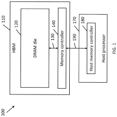
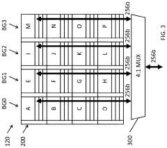
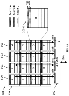
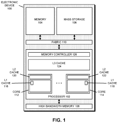
High-Bandwidth Memory (HBM) can be directly integrated with in-memory computing processors to significantly increase data transfer rates between memory and processing units. This integration reduces memory access latency and enables faster data processing for compute-intensive applications. The stacked memory architecture of HBM allows for wider memory buses and higher bandwidth compared to traditional memory solutions, making it ideal for in-memory computing where data movement is a critical bottleneck.- HBM integration with in-memory computing processors: High-Bandwidth Memory (HBM) can be directly integrated with in-memory computing processors to significantly increase data transfer rates and reduce latency. This integration typically involves stacking HBM dies on the same interposer as the processor using through-silicon vias (TSVs), creating a compact package that minimizes the physical distance between memory and processing elements. This architecture enables massive parallel data access and higher bandwidth compared to traditional DRAM configurations.
- Memory bandwidth optimization techniques for in-memory processors: Various techniques can be employed to optimize memory bandwidth in HBM-equipped in-memory computing systems. These include advanced memory controllers that efficiently manage data flow, intelligent prefetching algorithms that anticipate data needs, and memory access coalescing that combines multiple memory requests. Additionally, specialized memory addressing schemes and data compression techniques can be implemented to maximize effective bandwidth utilization while minimizing power consumption.
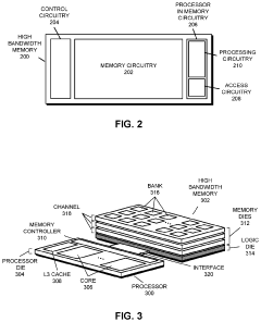
- 3D stacking and packaging technologies for HBM integration: Advanced 3D stacking and packaging technologies enable efficient integration of HBM with in-memory computing processors. These technologies include silicon interposers, wafer-level packaging, and advanced bonding techniques that allow for dense interconnections between memory and processor dies. The resulting 3D integrated circuits provide significantly higher memory bandwidth while maintaining a compact form factor, which is crucial for high-performance computing applications requiring intensive data processing.
- Neural network acceleration using HBM-based in-memory computing: HBM-based in-memory computing architectures can significantly accelerate neural network operations by performing computations directly within or near the memory arrays. This approach minimizes data movement between separate memory and processing units, which traditionally creates bottlenecks in neural network processing. By leveraging the high bandwidth of HBM and the parallelism of in-memory computing, these systems can achieve substantial performance improvements for AI workloads while reducing energy consumption.
- Memory hierarchy and caching strategies for HBM systems: Effective memory hierarchy design and caching strategies are crucial for maximizing the benefits of HBM in in-memory computing processors. These systems often employ multi-level cache architectures with specialized cache coherence protocols optimized for high-bandwidth memory access patterns. Smart data placement algorithms ensure that frequently accessed data resides in the fastest memory tiers, while less critical data can be stored in higher-capacity but lower-bandwidth memory layers, creating an optimal balance between performance and capacity.
02 3D stacking architecture for bandwidth optimization
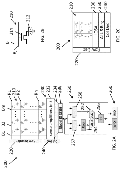
The three-dimensional stacking architecture of HBM enables significant bandwidth improvements for in-memory computing processors. By vertically stacking multiple DRAM dies and connecting them with through-silicon vias (TSVs), HBM provides much wider memory interfaces and shorter interconnects than traditional memory configurations. This architecture reduces signal degradation, lowers power consumption, and dramatically increases the available bandwidth for data-intensive computing tasks, making it particularly valuable for AI and machine learning applications.Expand Specific Solutions03 Memory controller designs for HBM in computing processors
Specialized memory controllers are designed to efficiently manage HBM in in-memory computing processors. These controllers optimize data movement between HBM stacks and processing elements, implement advanced scheduling algorithms to maximize bandwidth utilization, and manage thermal constraints. The controllers can dynamically adjust memory access patterns based on workload characteristics, prioritize critical data paths, and implement prefetching mechanisms to hide memory latency, resulting in improved overall system performance for in-memory computing applications.Expand Specific Solutions04 Power efficiency techniques for HBM-based in-memory computing
Various power efficiency techniques are implemented in HBM-based in-memory computing processors to manage the high power density of these systems. These include dynamic voltage and frequency scaling, selective activation of memory banks, power-aware data placement, and thermal management strategies. By optimizing power consumption while maintaining high bandwidth, these techniques enable more efficient in-memory computing solutions that can be deployed in various form factors with different thermal constraints.Expand Specific Solutions05 HBM interface optimization for specific computing workloads
HBM interfaces can be optimized for specific in-memory computing workloads to maximize effective bandwidth. This includes customized memory addressing schemes, specialized data compression techniques, and workload-specific memory access patterns. For AI and machine learning applications, optimizations might include tensor-oriented memory access, while for graph processing, different access patterns may be implemented. These optimizations ensure that the high bandwidth potential of HBM is fully utilized for the target computing applications.Expand Specific Solutions
Key Industry Players in HBM and IMC Ecosystems
High-Bandwidth Memory (HBM) integration in in-memory computing processors is currently in a growth phase, with the market expected to expand significantly as AI and data-intensive applications drive demand. The technology is approaching maturity with key players advancing different implementation strategies. Samsung Electronics and Micron Technology lead in HBM manufacturing, while Intel, AMD, and IBM are integrating HBM into their processor designs. Google and Meta are developing custom solutions for their data centers. Emerging players like Graphcore and AvicenaTech are introducing innovative architectures, while Chinese companies including Cambricon and ChangXin Memory are rapidly advancing their capabilities. TSMC provides critical manufacturing support across the ecosystem. The competitive landscape is characterized by established semiconductor giants competing with specialized AI chip startups and hyperscalers developing proprietary solutions.
Samsung Electronics Co., Ltd.
Technical Solution: Samsung has pioneered HBM integration in computing processors through their Aquabolt HBM2 technology, which achieves data transfer rates of up to 2.4 Gbps per pin. Their approach combines HBM stacks with processing elements using advanced 2.5D and 3D packaging technologies. Samsung's Processing-in-Memory (PIM) architecture integrates computing capabilities directly into HBM, enabling data processing where it resides. Their HBM-PIM solution incorporates AI processing units within the memory, reducing data movement and achieving up to 2x performance improvement and 70% energy reduction in AI workloads[1]. Samsung has also developed a programmable PIM architecture that supports standard frameworks like TensorFlow, making the technology more accessible to developers without requiring specialized knowledge of memory systems.
Strengths: Vertical integration as both memory manufacturer and system designer; industry-leading HBM fabrication capabilities; mature 2.5D/3D packaging technologies. Weaknesses: Proprietary solutions may limit ecosystem adoption; higher cost compared to conventional memory solutions; thermal management challenges in dense HBM-processor integration.
Micron Technology, Inc.
Technical Solution: Micron has developed a comprehensive HBM integration strategy for in-memory computing through their Hybrid Memory Cube (HMC) technology and more recent HBM implementations. Their approach features a logic layer at the base of the memory stack that contains specialized processing elements for data-intensive operations. Micron's Automata Processor technology, integrated with HBM, enables high-throughput pattern matching directly within memory structures. Their latest HBM solutions achieve bandwidth exceeding 900 GB/s per stack with significantly reduced power consumption compared to traditional DRAM architectures[2]. Micron has also pioneered heterogeneous integration techniques that combine HBM with compute dies using silicon interposers, enabling ultra-wide bus widths (up to 1024 bits) while maintaining signal integrity across the interface.
Strengths: Extensive memory manufacturing expertise; pioneering work in 3D stacked memory architectures; strong IP portfolio in memory-centric computing. Weaknesses: Less vertical integration than competitors with both processor and memory capabilities; higher implementation complexity requiring specialized design expertise; thermal constraints in high-density configurations.
Critical Patents and Innovations in HBM-IMC Integration
Systems and methods for data placement for in-memory-compute
PatentActiveUS20240004646A1
Innovation
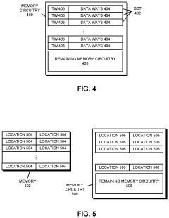
- Integration of an in-memory compute (IMC) module within the DRAM banks, featuring an arithmetic logic unit (ALU) and a memory controller that manages data layout and performs computations directly within the memory module, reducing reliance on external buses by optimizing data placement within DRAM banks.
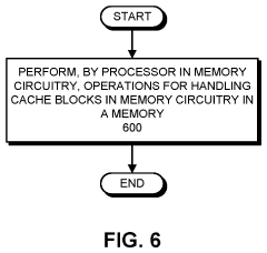
Performing Operations for Handling Data using Processor in Memory Circuitry in a High Bandwidth Memory
PatentPendingUS20230359556A1
Innovation
- Implementing processor in memory (PIM) circuitry within high bandwidth memory to perform cache operations and handle data, reducing the need for processors to handle these tasks directly, thereby offloading operations and improving performance.
Thermal Management Strategies for HBM-IMC Systems
The integration of High-Bandwidth Memory (HBM) with In-Memory Computing (IMC) processors creates significant thermal challenges that require innovative management strategies. As power densities increase with the stacking of memory dies and computational elements, heat dissipation becomes a critical bottleneck affecting both performance and reliability of HBM-IMC systems.
Conventional cooling solutions prove inadequate for these advanced architectures due to the three-dimensional nature of HBM stacks and their proximity to processing elements. The thermal interface materials (TIMs) between stacked dies create additional thermal resistance, exacerbating heat accumulation within the system. Moreover, the heterogeneous nature of HBM-IMC systems results in non-uniform heat distribution, creating hotspots that can lead to thermal throttling and reduced system performance.
Advanced liquid cooling solutions have emerged as promising approaches for HBM-IMC thermal management. Direct liquid cooling to the processor package can remove heat more efficiently than traditional air cooling methods. Two-phase cooling systems utilizing the latent heat of vaporization offer even greater cooling capacity for high-power density applications. Some research prototypes have demonstrated microfluidic cooling channels integrated directly into silicon interposers, enabling heat removal closer to the source.
Dynamic thermal management (DTM) techniques complement hardware cooling solutions by intelligently controlling system operation based on thermal conditions. These include workload migration algorithms that redistribute computational tasks to cooler regions of the chip and dynamic voltage and frequency scaling (DVFS) that adjusts processor performance to maintain safe operating temperatures. Thermal-aware memory access scheduling further optimizes system operation by considering the thermal impact of memory operations.
Novel materials are also playing a crucial role in thermal management innovation. Diamond-based TIMs with thermal conductivity up to five times higher than conventional materials significantly improve heat transfer between stacked dies. Graphene heat spreaders effectively distribute heat laterally across the package, reducing hotspot formation. Additionally, phase-change materials incorporated into the package absorb heat during high-load operations and release it during idle periods, effectively dampening thermal fluctuations.
3D packaging technologies specifically designed for thermal optimization represent another frontier in HBM-IMC thermal management. Through-silicon vias (TSVs) can be strategically placed to create thermal pathways that channel heat away from critical components. Some advanced designs incorporate dedicated thermal TSVs filled with high-conductivity materials solely for heat dissipation purposes.
Power Efficiency Considerations in HBM-IMC Designs
Power efficiency represents a critical challenge in the integration of High-Bandwidth Memory (HBM) with In-Memory Computing (IMC) processors. The inherent power demands of HBM interfaces, coupled with the computational requirements of IMC architectures, create a complex power management landscape that designers must carefully navigate.
Current HBM-IMC designs typically consume between 20-30W for memory operations alone, with additional power required for computational functions. This significant power envelope necessitates sophisticated thermal management solutions and can limit deployment scenarios, particularly in edge computing applications where power constraints are stringent.
Several architectural approaches have emerged to address these power efficiency challenges. Dynamic voltage and frequency scaling (DVFS) techniques allow for real-time adjustment of power consumption based on workload demands, potentially reducing power consumption by 15-25% during low-utilization periods. Granular power gating mechanisms enable selective deactivation of unused memory banks or computational units, further optimizing energy usage.
Advanced 3D integration techniques are showing promise in reducing power requirements through shorter interconnect distances. By minimizing the physical separation between memory and processing elements, signal integrity improves while reducing the power needed for data movement. Recent implementations have demonstrated up to 40% reduction in power consumption for data transfer operations compared to traditional 2.5D integration approaches.
Emerging memory controller designs incorporate sophisticated power-aware scheduling algorithms that prioritize operations based on both performance requirements and energy considerations. These controllers can dynamically adjust refresh rates, optimize access patterns, and coordinate data movement to minimize overall system power while maintaining performance targets.
Thermal considerations remain paramount, as power density in HBM-IMC designs can exceed 1W/mm² in active regions. Innovative cooling solutions, including integrated liquid cooling channels and phase-change materials, are being explored to manage thermal dissipation more efficiently than traditional approaches.
The industry is increasingly adopting standardized power modeling frameworks to enable accurate prediction of power consumption during the design phase. These models incorporate workload-specific characteristics and can guide architectural decisions to optimize for specific application domains, potentially reducing overall system power by 10-30% compared to general-purpose designs.
Unlock deeper insights with Patsnap Eureka Quick Research — get a full tech report to explore trends and direct your research. Try now!
Generate Your Research Report Instantly with AI Agent
Supercharge your innovation with Patsnap Eureka AI Agent Platform!