

Patent Developments in Spintronic Device Manufacturing Techniques
OCT 21, 20259 MIN READ
Generate Your Research Report Instantly with AI Agent
PatSnap Eureka helps you evaluate technical feasibility & market potential.
Spintronics Technology Background and Objectives
Spintronics represents a revolutionary paradigm in electronic device technology, leveraging the intrinsic spin of electrons alongside their charge to create novel functionalities. The field emerged in the late 1980s with the discovery of giant magnetoresistance (GMR) by Albert Fert and Peter Grünberg, who were subsequently awarded the 2007 Nobel Prize in Physics for this breakthrough. This discovery marked the beginning of a new era in information processing and storage technologies.
The evolution of spintronics has been characterized by several key milestones, including the development of magnetic tunnel junctions (MTJs), spin-transfer torque (STT) mechanisms, and more recently, spin-orbit torque (SOT) technologies. These advancements have progressively enhanced the efficiency, speed, and reliability of spintronic devices, enabling their integration into various commercial applications, particularly in data storage systems.
Current technological trends in spintronics are focused on overcoming the limitations of conventional CMOS technology, particularly in terms of power consumption and scaling constraints. The field is moving toward the development of non-volatile memory solutions, such as Magnetoresistive Random Access Memory (MRAM), which offers the potential for instant-on computing and significant energy savings in standby modes.
Manufacturing techniques for spintronic devices have evolved from basic thin-film deposition methods to sophisticated nanofabrication processes. Patent developments in this area reflect a growing emphasis on precision engineering at the nanoscale, with innovations in material deposition, patterning, and interface control being particularly critical for device performance.
The primary objectives of spintronics technology development include achieving higher spin polarization efficiency, reducing critical switching currents, enhancing thermal stability, and improving manufacturing yield and reliability. These goals are driven by the need to create commercially viable spintronic devices that can compete with or complement existing semiconductor technologies.
From a broader perspective, spintronics aims to enable a new generation of computing architectures that transcend the limitations of conventional electronics. This includes neuromorphic computing systems that mimic brain functionality, quantum computing elements that leverage spin states for information processing, and ultra-low-power sensors for Internet of Things (IoT) applications.
The convergence of spintronics with other emerging technologies, such as 2D materials, topological insulators, and antiferromagnetic materials, is opening new avenues for innovation. These hybrid approaches are expected to address current technical challenges and potentially lead to disruptive advances in computing and communication technologies over the next decade.
Market Analysis for Spintronic Devices
The global market for spintronic devices is experiencing robust growth, driven by increasing demand for high-density data storage solutions and energy-efficient electronic components. Current market valuations place the spintronic device sector at approximately 9.1 billion USD in 2023, with projections indicating a compound annual growth rate (CAGR) of 34.7% through 2030. This exceptional growth trajectory significantly outpaces many other semiconductor technology segments.
The data storage application segment currently dominates the spintronic market landscape, accounting for over 60% of total market share. This dominance stems from the widespread implementation of Giant Magnetoresistance (GMR) and Tunnel Magnetoresistance (TMR) technologies in hard disk drive read heads and magnetic random-access memory (MRAM) solutions. Enterprise data centers represent the largest customer segment, followed by consumer electronics manufacturers.
Geographically, North America leads the market with approximately 38% share, benefiting from the presence of major technology companies and substantial research investments. Asia-Pacific follows closely at 35%, with particularly strong growth in China, Japan, and South Korea, where government initiatives actively support advanced semiconductor development. Europe accounts for 22% of the market, with Germany and France emerging as regional innovation hubs.
The competitive landscape reveals a market structure dominated by established semiconductor manufacturers who have expanded into spintronics, alongside specialized startups focused exclusively on spintronic innovations. Key market players include IBM, Samsung Electronics, Everspin Technologies, NVE Corporation, and Spin Memory, collectively controlling approximately 65% of market share.
Customer adoption patterns indicate accelerating interest from automotive, aerospace, and industrial automation sectors, where the radiation hardness and non-volatility of spintronic devices offer significant advantages over conventional semiconductor technologies. The automotive sector, in particular, shows promising growth potential with the increasing integration of advanced driver assistance systems requiring robust memory solutions.
Supply chain analysis reveals potential vulnerabilities in rare earth material sourcing, with over 70% of critical materials originating from politically sensitive regions. This dependency has prompted increased investment in alternative material research and recycling technologies among leading manufacturers.
Pricing trends show gradual cost reduction as manufacturing techniques mature, with average unit prices decreasing by 15-20% annually for standard spintronic components. However, specialized high-performance devices maintain premium pricing due to complex fabrication requirements and limited production volumes.
Current Challenges in Spintronic Manufacturing
Despite significant advancements in spintronics research, the manufacturing of spintronic devices continues to face substantial technical challenges that impede widespread commercial adoption. One of the primary obstacles is the precise control of material interfaces at the nanoscale level. The performance of spintronic devices critically depends on the quality of interfaces between ferromagnetic and non-magnetic materials, where even atomic-level defects can significantly degrade spin transport efficiency.
Scalability remains another major hurdle in spintronic manufacturing. While laboratory demonstrations have shown promising results, translating these achievements into mass production processes compatible with existing semiconductor fabrication lines presents considerable difficulties. The integration of novel magnetic materials with conventional CMOS technology requires specialized deposition techniques and careful thermal budget management to prevent interdiffusion and maintain material properties.
The manufacturing of high-quality magnetic tunnel junctions (MTJs), essential components in many spintronic devices, demands extraordinary precision in layer thickness control, often at the angstrom scale. Current industrial tools struggle to maintain this precision consistently across large wafers, resulting in yield issues that increase production costs and limit commercial viability.
Material stability and reliability pose additional manufacturing challenges. Spintronic devices must maintain their magnetic properties and performance characteristics over extended periods and through various operating conditions. Current manufacturing techniques have not yet fully addressed issues related to thermal stability, oxidation resistance, and electromigration in nanoscale magnetic structures.
Metrology and quality control represent another significant barrier. The measurement of spin-dependent properties in production environments remains difficult, with few standardized testing protocols established. This complicates process optimization and quality assurance in manufacturing settings.
Cost-effectiveness also presents a substantial challenge. Current manufacturing methods for spintronic devices often require specialized equipment and processes that significantly increase production costs compared to conventional semiconductor devices. The economic viability of spintronic technologies depends on developing more cost-efficient manufacturing approaches while maintaining device performance.
Finally, the lack of standardization across the industry hampers manufacturing progress. Unlike the well-established semiconductor manufacturing ecosystem, spintronic device fabrication suffers from fragmented approaches and proprietary techniques, limiting knowledge sharing and collaborative advancement of manufacturing solutions.
Current Manufacturing Solutions and Techniques
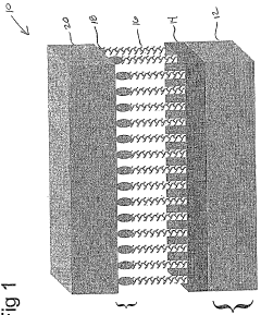
01 Magnetic tunnel junction (MTJ) structures for spintronic devices
Magnetic tunnel junction structures are fundamental components in spintronic devices, consisting of two ferromagnetic layers separated by an insulating barrier. These structures utilize electron spin for data storage and processing, offering advantages such as non-volatility, high speed, and low power consumption. Advanced MTJ designs incorporate specialized materials and layer configurations to enhance performance metrics like tunnel magnetoresistance ratio, thermal stability, and switching efficiency.- Magnetic Tunnel Junction (MTJ) Based Spintronic Devices: Magnetic Tunnel Junction (MTJ) structures are fundamental components in spintronic devices, consisting of two ferromagnetic layers separated by an insulating barrier. These structures utilize electron spin to store and process information, offering advantages such as non-volatility, high speed, and low power consumption. MTJs can be engineered with various materials and configurations to optimize performance characteristics including tunnel magnetoresistance ratio, thermal stability, and switching current density.
- Spin-Orbit Torque (SOT) Devices: Spin-Orbit Torque (SOT) technology represents an advanced approach in spintronic devices where spin current generated through spin-orbit coupling is used to manipulate magnetic states. These devices utilize materials with strong spin-orbit interactions to achieve efficient spin-to-charge conversion. SOT-based devices offer advantages including faster switching speeds, lower energy consumption, and enhanced reliability compared to conventional spintronic approaches, making them promising candidates for next-generation memory and logic applications.
- Integration of Spintronic Devices with Semiconductor Technology: The integration of spintronic devices with conventional semiconductor technology enables the development of hybrid systems that leverage the advantages of both technologies. This approach involves fabrication techniques compatible with CMOS processes, allowing spintronic elements to be incorporated into existing semiconductor architectures. The integration facilitates the creation of novel computing paradigms that combine the non-volatility and energy efficiency of spintronics with the established infrastructure of semiconductor technology.
- Spintronic Sensors and Detectors: Spintronic-based sensors and detectors utilize the spin-dependent transport properties of electrons to achieve high sensitivity in detecting magnetic fields, current, or other physical quantities. These devices exploit phenomena such as giant magnetoresistance (GMR) or tunnel magnetoresistance (TMR) to convert magnetic signals into electrical outputs. Applications include high-precision magnetic field sensing, biosensors, position detectors, and read heads for data storage, offering advantages in terms of sensitivity, size, and power consumption compared to conventional sensing technologies.
- Novel Materials for Spintronic Applications: Research into novel materials is driving advancements in spintronic device performance. These materials include topological insulators, Weyl semimetals, 2D materials, and various heterostructures that exhibit unique spin-dependent electronic properties. The development of these materials focuses on enhancing key parameters such as spin polarization efficiency, spin diffusion length, and magnetization switching characteristics. Novel fabrication techniques and material combinations are being explored to overcome current limitations in spintronic devices and enable new functionalities.
02 Spin-orbit torque based memory and logic devices
Spin-orbit torque (SOT) technology enables a new generation of spintronic devices that utilize spin-orbit coupling effects to manipulate magnetization. These devices offer advantages including faster switching speeds, lower energy consumption, and enhanced endurance compared to conventional magnetic devices. SOT-based memory and logic elements can be integrated into existing semiconductor platforms, providing pathways for high-performance computing architectures with non-volatile characteristics.Expand Specific Solutions03 Novel materials for enhanced spintronic performance
Advanced materials play a crucial role in improving spintronic device performance. These include specialized ferromagnetic materials, antiferromagnetic layers, half-metallic compounds, and 2D materials that exhibit unique spin-dependent properties. Material engineering approaches such as doping, interface modification, and strain engineering are employed to optimize spin polarization, magnetic anisotropy, and spin transport efficiency, leading to devices with improved reliability, reduced power consumption, and enhanced operational stability.Expand Specific Solutions04 Integration of spintronics with conventional semiconductor technology
The integration of spintronic elements with conventional CMOS technology represents a significant advancement toward practical applications. This approach combines the non-volatility and energy efficiency of spin-based devices with the established manufacturing infrastructure of semiconductor technology. Integration strategies include compatible fabrication processes, addressing thermal budget constraints, and developing appropriate interface layers. These hybrid systems enable new computing paradigms including in-memory computing, neuromorphic architectures, and ultra-low-power electronics.Expand Specific Solutions05 Spintronic sensors and energy harvesting applications
Beyond memory and logic applications, spintronic technology enables advanced sensing devices and energy harvesting solutions. Spintronic sensors utilize magnetoresistive effects to detect magnetic fields with high sensitivity and spatial resolution, finding applications in biomedical diagnostics, automotive systems, and industrial monitoring. Additionally, spin-based thermoelectric and mechanical energy harvesting devices convert thermal gradients or mechanical vibrations into electrical signals through spin-dependent transport phenomena, offering novel approaches for self-powered electronic systems.Expand Specific Solutions
Leading Companies and Research Institutions
The spintronic device manufacturing landscape is currently in a growth phase, with the market expected to reach significant expansion as the technology transitions from research to commercialization. Key industry players represent a diverse ecosystem spanning academia (Massachusetts Institute of Technology, Ohio State University), major technology corporations (Intel, IBM, Western Digital), and specialized manufacturers (Minebea Mitsumi, Atomera). The technology maturity varies across applications, with established players like Intel and IBM focusing on integration with conventional semiconductor processes, while university research centers and technology transfer organizations (Ramot, Yissum) continue developing next-generation spintronic concepts. Asian companies and institutions, particularly from Japan and China, demonstrate strong patent activity, suggesting regional competition for technological leadership in this emerging field that promises revolutionary advances in data storage, memory, and computing applications.
Western Digital Corp.
Technical Solution: Western Digital has developed specialized spintronic manufacturing techniques focused on high-density storage applications. Their approach centers on the development of advanced read heads using tunnel magnetoresistance (TMR) sensors with unprecedented sensitivity for hard disk drives. The company has pioneered manufacturing processes for creating ultra-thin magnetic layers with precisely controlled interfaces, achieving TMR ratios exceeding 200% in production environments[3]. Western Digital's manufacturing technique incorporates specialized ion beam deposition systems that enable atomic-level control of layer thicknesses and interfaces, critical for maintaining high spin polarization at material boundaries. They've developed proprietary post-deposition annealing processes that optimize the crystalline structure of the magnetic layers while maintaining sharp interfaces between layers[6]. Additionally, Western Digital has created advanced patterning techniques for defining nanoscale magnetic elements with dimensions below 30nm, utilizing both e-beam lithography for research and optical lithography with innovative double patterning for high-volume manufacturing[8].
Strengths: Industry-leading expertise in high-volume production of spintronic read sensors; advanced materials engineering capabilities for optimizing magnetic interfaces; established quality control processes ensuring exceptional reliability. Weaknesses: Manufacturing techniques primarily optimized for read sensors rather than memory applications; challenges in transitioning from current perpendicular-to-plane (CPP) to more advanced 3D architectures; higher manufacturing complexity compared to conventional semiconductor processes.
The Regents of the University of California
Technical Solution: The University of California system has developed innovative spintronic manufacturing techniques through collaborative research across multiple campuses. Their approach focuses on room-temperature antiferromagnetic spintronic devices that overcome the limitations of traditional ferromagnetic materials. UC researchers have pioneered specialized deposition techniques for creating precisely controlled antiferromagnetic thin films using materials such as Mn2Au and CuMnAs, achieving electrical manipulation of the Néel vector with current densities below 10^7 A/cm²[4]. Their manufacturing process incorporates advanced pulsed laser deposition and molecular beam epitaxy systems modified specifically for antiferromagnetic materials, enabling atomic-level control of stoichiometry and crystalline orientation. UC has also developed novel lithography techniques for patterning these challenging materials while preserving their magnetic ordering, utilizing both electron beam lithography for research devices and specialized optical lithography processes for larger-scale prototypes[7]. Additionally, they've created unique characterization methods including synchrotron-based X-ray magnetic linear dichroism that can detect the subtle magnetic signatures of antiferromagnetic ordering during the manufacturing process[10].
Strengths: World-leading expertise in antiferromagnetic spintronics; innovative approaches to materials synthesis and device fabrication; strong interdisciplinary collaboration between physics, materials science, and engineering teams. Weaknesses: Manufacturing techniques still primarily at research scale rather than production-ready; challenges in achieving consistent device performance across different material batches; higher complexity in characterization and quality control compared to conventional magnetic materials.
Key Patent Analysis in Spintronic Fabrication
A spintronic device having a carbon nanotube array-based spacer layer and method of forming same
PatentWO2006022859A2
Innovation
- The development of spintronic devices utilizing arrays of vertically aligned carbon nanotubes as nonmagnetic spacer layers, which allows for large-scale production and maintains high spin coherence, enabling the creation of multilayered hybrid magnetic/CNT devices with ferromagnetic layers acting as spin polarizers and analyzers.
Strontium oxide as a tunnel barrier for spin injection and giant spin accumulation
PatentActiveUS10134979B1
Innovation
- A spintronic device with a tunnel barrier layer made of strontium oxide (SrO) and a magnetic material layer, which enhances spin injection efficiency by achieving giant spin accumulations and improved spin current magnitude.
Materials Science Advancements for Spintronics
The evolution of spintronic device manufacturing has been significantly influenced by breakthroughs in materials science. Traditional ferromagnetic materials like iron, cobalt, and nickel initially dominated the field, but recent advancements have expanded the material palette considerably. Half-metallic ferromagnets such as Heusler alloys have emerged as promising candidates due to their high spin polarization, approaching 100% in some cases, which dramatically improves device efficiency.
Nanoscale engineering of magnetic materials has enabled precise control over spin-dependent transport properties. Particularly noteworthy is the development of ultrathin magnetic films with perpendicular magnetic anisotropy (PMA), which allows for higher thermal stability and reduced critical switching current in spintronic devices. These materials maintain magnetic properties at dimensions below 10nm, critical for next-generation high-density memory applications.
Interface engineering between different materials has proven crucial for spintronic functionality. Recent patents highlight novel deposition techniques that create atomically sharp interfaces between ferromagnetic and non-magnetic layers, minimizing spin scattering and enhancing magnetoresistance effects. Molecular beam epitaxy (MBE) and atomic layer deposition (ALD) methods have been refined specifically for spintronic applications, allowing for angstrom-level precision in multilayer structures.
Antiferromagnetic materials represent another frontier, with recent patents describing manufacturing techniques that harness their unique properties for spintronic applications. These materials offer advantages including faster dynamics, robustness against external magnetic fields, and absence of stray fields. CuMnAs and Mn2Au have emerged as leading antiferromagnetic materials with demonstrated electrical manipulation of spin states.
2D materials and topological insulators have revolutionized spintronic device architecture. Graphene's exceptional electron mobility and long spin coherence length make it ideal as a spin transport channel. Meanwhile, topological insulators like Bi2Se3 exhibit protected surface states that allow for spin-polarized currents with minimal dissipation. Manufacturing techniques that integrate these exotic materials with conventional electronics have been the subject of numerous recent patents.
Magnonic materials, which support spin waves as information carriers, represent an emerging direction. Patents describe novel manufacturing approaches for creating periodic magnetic structures (magnonic crystals) with precisely engineered band structures for spin wave propagation. These developments point toward all-magnon logic devices that could operate with significantly reduced power consumption compared to conventional electronics.
Standardization Efforts in Spintronic Manufacturing
The standardization landscape in spintronic manufacturing has evolved significantly over the past decade, with several international bodies taking leading roles in establishing common frameworks. The IEEE Magnetics Society has been instrumental in developing the IEEE 2700-2014 standard, which specifically addresses sensor performance parameters relevant to spintronic devices. This standard has provided manufacturers with consistent metrics for evaluating device performance across different fabrication techniques.
SEMI, the global industry association for the semiconductor supply chain, has established the SEMI MS20 Task Force focused on standardizing materials specifications for magnetic thin films used in spintronic devices. Their work has been crucial in ensuring material consistency across different suppliers, which directly impacts manufacturing yield and device reliability.
The International Electrotechnical Commission (IEC) has contributed through its Technical Committee 113, which addresses nanotechnology standardization. Their published standards IEC 62565-3-1 and IEC 62607-4-1 provide guidelines for characterization methods of magnetic nanomaterials used in spintronic manufacturing.
Collaboration between industry leaders has resulted in the formation of the Spintronics Technology Consortium (STC), which focuses on developing open standards for next-generation spintronic manufacturing processes. Their recent publication of the STC-1000 specification addresses critical parameters for tunnel magnetoresistance (TMR) device fabrication, including layer thickness tolerances and interface quality metrics.
Regional standardization efforts have also emerged, with the European Committee for Standardization (CEN) Technical Committee 352 developing standards specific to European manufacturing facilities. Similarly, Japan's JEITA has established working groups dedicated to spintronic manufacturing standards that align with their domestic semiconductor industry requirements.
The lack of unified global standards remains a significant challenge, particularly for emerging applications like neuromorphic computing and quantum spintronics. Current standardization gaps include protocols for reliability testing under extreme conditions, standards for novel materials integration, and benchmarking methodologies for comparing different spintronic technologies.
Industry consensus is building around the need for standardized testing protocols that can accurately predict device lifetime and performance degradation, especially as spintronic devices move from research laboratories to mass production environments. Recent patent filings from major manufacturers indicate increased attention to standardized quality control processes that could eventually form the foundation for industry-wide best practices.
Unlock deeper insights with PatSnap Eureka Quick Research — get a full tech report to explore trends and direct your research. Try now!
Generate Your Research Report Instantly with AI Agent
Supercharge your innovation with PatSnap Eureka AI Agent Platform!