

Photonic crystal structure integration in AMOLED for durability.
JUL 17, 20259 MIN READ
Generate Your Research Report Instantly with AI Agent
PatSnap Eureka helps you evaluate technical feasibility & market potential.
Photonic Crystal AMOLED Integration Background
Photonic crystal structures have emerged as a promising technology for enhancing the durability and performance of Active-Matrix Organic Light-Emitting Diode (AMOLED) displays. The integration of these structures into AMOLED devices represents a significant advancement in display technology, addressing key challenges in the field.
AMOLED displays have gained popularity due to their superior image quality, energy efficiency, and flexibility. However, they face durability issues, particularly in terms of susceptibility to environmental factors and degradation over time. The incorporation of photonic crystal structures aims to mitigate these challenges and extend the lifespan of AMOLED devices.
Photonic crystals are periodic nanostructures that can manipulate the flow of light at the wavelength scale. By carefully designing these structures, it is possible to control the emission and propagation of light within the AMOLED device. This control offers several potential benefits, including improved light extraction efficiency, enhanced color purity, and increased resistance to external factors that can degrade the organic materials.
The concept of integrating photonic crystals into AMOLED displays builds upon decades of research in both photonics and organic electronics. Early work in photonic crystals dates back to the 1980s, with significant advancements in fabrication techniques and theoretical understanding occurring in the 1990s and 2000s. Concurrently, OLED technology has evolved rapidly since its inception in the 1980s, with AMOLED displays becoming commercially viable in the early 2000s.
The convergence of these two fields presents an opportunity to address the inherent limitations of AMOLED technology. By incorporating photonic crystal structures, researchers aim to create more robust displays that can withstand harsh environmental conditions and maintain their performance characteristics over extended periods.
The integration process involves careful consideration of the photonic crystal design, material selection, and fabrication techniques. Researchers must balance the optical properties of the photonic crystal with the electrical and chemical requirements of the AMOLED structure. This interdisciplinary approach draws upon expertise in optics, materials science, and device engineering.
As the demand for high-performance, durable displays continues to grow across various industries, including consumer electronics, automotive, and healthcare, the development of photonic crystal-integrated AMOLED technology has gained significant momentum. This innovative approach holds the potential to revolutionize display technology, offering improved durability without compromising the inherent advantages of AMOLED displays.
AMOLED Durability Market Demand
The integration of photonic crystal structures in AMOLED displays for enhanced durability has sparked significant market interest due to the growing demand for more robust and long-lasting display technologies. As consumers increasingly rely on mobile devices and wearable technology, the need for durable AMOLED displays has become paramount, driving market growth and innovation in this sector.
The global AMOLED market has been experiencing rapid expansion, with a particular focus on durability as a key differentiator. This trend is fueled by the rising adoption of AMOLED displays in smartphones, smartwatches, and other portable devices that are prone to daily wear and tear. Consumers are willing to pay a premium for devices that offer superior longevity and resistance to damage, creating a strong market pull for durability-enhancing technologies like photonic crystal structures.
In the automotive industry, there is a growing demand for AMOLED displays in dashboard and infotainment systems. These applications require displays that can withstand harsh environmental conditions, including extreme temperatures and prolonged exposure to sunlight. The integration of photonic crystal structures in AMOLED displays for improved durability aligns perfectly with the automotive sector's stringent requirements, opening up new market opportunities.
The healthcare and medical device markets also present significant potential for durable AMOLED displays. Medical equipment, such as patient monitors and portable diagnostic devices, demands displays that can endure frequent cleaning and disinfection without degradation. The incorporation of photonic crystal structures can enhance the chemical resistance of AMOLED displays, making them more suitable for these critical applications.
Market research indicates that consumers are becoming increasingly aware of the environmental impact of electronic devices. This awareness has led to a preference for more durable products that have longer lifespans, reducing electronic waste. AMOLED displays with integrated photonic crystal structures for improved durability cater to this eco-conscious market segment, potentially driving adoption rates and market growth.
The enterprise and industrial sectors represent another area of significant market demand for durable AMOLED displays. In these environments, devices are often subjected to harsh conditions and heavy usage. The integration of photonic crystal structures can enhance the resilience of AMOLED displays, making them more suitable for use in factories, warehouses, and other industrial settings where durability is crucial.
As the market for foldable and flexible displays continues to expand, the need for durable AMOLED technology becomes even more critical. These innovative form factors introduce new challenges in terms of display longevity and resistance to repeated folding and unfolding. Photonic crystal structures could play a vital role in addressing these challenges, potentially accelerating the adoption of foldable devices across various consumer and professional markets.
Photonic Crystal Challenges in AMOLED
The integration of photonic crystal structures in AMOLED displays presents several significant challenges that researchers and engineers must overcome to enhance durability and performance. One of the primary obstacles is achieving precise control over the fabrication process of photonic crystals at the nanoscale level. The intricate nature of these structures demands extremely high accuracy in manufacturing, which can be difficult to maintain consistently across large-scale production.
Another major challenge lies in the compatibility between photonic crystal materials and existing AMOLED components. The introduction of new materials and structures must not compromise the functionality or efficiency of the OLED layers. This requires careful consideration of material properties, such as thermal stability, chemical reactivity, and optical characteristics, to ensure seamless integration without degrading the overall display performance.
The durability of photonic crystal structures under various environmental conditions poses yet another hurdle. AMOLED displays are subjected to temperature fluctuations, humidity, and mechanical stress during regular use. Ensuring that the photonic crystal structures can withstand these factors without deterioration or loss of optical properties is crucial for long-term device reliability.
Furthermore, the challenge of maintaining color accuracy and consistency across the display becomes more complex with the integration of photonic crystals. These structures can significantly alter the emission spectrum and angular distribution of light from OLEDs. Achieving uniform color reproduction and maintaining wide viewing angles while leveraging the benefits of photonic crystals requires sophisticated optical design and careful tuning of the crystal parameters.
Power efficiency is another critical aspect that faces challenges with photonic crystal integration. While these structures have the potential to enhance light extraction and reduce power consumption, optimizing their design to maximize energy efficiency without compromising other display qualities remains a complex task. Balancing the trade-offs between improved light outcoupling and potential increases in production costs or complexity is essential for commercial viability.
Lastly, the scalability of photonic crystal integration techniques to large-area displays presents a significant challenge. Methods that work well for small prototypes may not be directly applicable to mass production of large screens. Developing cost-effective and reliable manufacturing processes that can maintain the precision and quality of photonic crystal structures over large areas is crucial for widespread adoption in the AMOLED industry.
Current Photonic Crystal Integration Solutions
01 Protective coatings for photonic crystal structures
Applying protective coatings to photonic crystal structures can significantly enhance their durability. These coatings can protect against environmental factors, mechanical stress, and chemical degradation, thereby extending the lifespan of the photonic crystal structure. Various materials and techniques can be used for coating, depending on the specific application and environmental conditions.- Protective coatings for photonic crystal structures: Applying protective coatings to photonic crystal structures can significantly enhance their durability. These coatings can protect against environmental factors, mechanical stress, and chemical degradation, thereby extending the lifespan of the photonic crystal structure. Various materials and techniques can be used to create these protective layers, including polymer coatings, inorganic films, and hybrid materials.
- Structural reinforcement techniques: Implementing structural reinforcement techniques can improve the durability of photonic crystal structures. This may involve optimizing the crystal lattice design, incorporating support structures, or using materials with enhanced mechanical properties. These techniques can help the structure withstand physical stresses and maintain its optical properties over time.
- Temperature-resistant photonic crystal designs: Developing temperature-resistant photonic crystal designs is crucial for enhancing durability in high-temperature applications. This can involve using materials with high melting points, incorporating thermal management systems, or designing structures that can withstand thermal expansion and contraction without losing their optical properties.
- Self-healing photonic crystal structures: Incorporating self-healing mechanisms into photonic crystal structures can significantly improve their durability. These mechanisms allow the structure to repair minor damage autonomously, potentially extending its lifespan and maintaining its optical properties over time. This can involve the use of smart materials or the integration of repair agents within the structure.
- Environmental resistance enhancements: Improving the environmental resistance of photonic crystal structures is essential for their long-term durability. This can involve developing structures that are resistant to moisture, UV radiation, and chemical exposure. Techniques may include surface treatments, material selection, and encapsulation methods to protect the structure from environmental degradation.
02 Structural reinforcement techniques
Implementing structural reinforcement techniques can improve the durability of photonic crystal structures. This may involve optimizing the crystal lattice design, incorporating supporting elements, or using composite materials to enhance mechanical strength. Such reinforcements can help the structure withstand physical stresses and maintain its optical properties over time.Expand Specific Solutions03 Temperature-resistant photonic crystal designs
Developing temperature-resistant photonic crystal designs is crucial for enhancing durability in high-temperature applications. This involves selecting materials with high thermal stability, optimizing the crystal structure to minimize thermal expansion effects, and incorporating heat-dissipation mechanisms. Such designs can maintain their optical properties and structural integrity under extreme temperature conditions.Expand Specific Solutions04 Self-healing photonic crystal structures
Incorporating self-healing mechanisms into photonic crystal structures can significantly improve their long-term durability. These mechanisms may involve the use of smart materials that can repair minor damages autonomously, or the integration of self-repairing nanostructures. Such self-healing capabilities can extend the operational life of photonic crystal devices in challenging environments.Expand Specific Solutions05 Environmental isolation techniques
Implementing environmental isolation techniques can protect photonic crystal structures from external factors that may compromise their durability. This may include encapsulation methods, hermetic sealing, or the use of protective packaging. By shielding the structure from moisture, contaminants, and other environmental stressors, these techniques can significantly enhance the longevity and reliability of photonic crystal devices.Expand Specific Solutions
Key Players in Photonic Crystal AMOLED
The integration of photonic crystal structures in AMOLED for durability is an emerging technology in the display industry, currently in its early development stage. The market for this technology is expected to grow significantly as manufacturers seek to enhance the longevity and performance of AMOLED displays. While the market size is still relatively small, it shows promising potential for expansion. In terms of technological maturity, companies like Samsung Electronics, BOE Technology Group, and Sharp Corp. are at the forefront of research and development. These industry leaders are investing heavily in advancing photonic crystal integration techniques, aiming to overcome challenges related to manufacturing scalability and cost-effectiveness. As the technology progresses, we can expect increased competition and innovation from other major players in the display industry.
BOE Technology Group Co., Ltd.
Technical Solution: BOE has developed a proprietary photonic crystal integration technique for AMOLED displays focused on durability enhancement. Their approach involves creating a multi-layered photonic crystal structure that is seamlessly integrated into the OLED stack. This structure is designed to provide both optical and physical benefits. Optically, it enhances light outcoupling efficiency by up to 25% [2], improving overall display brightness and energy efficiency. Physically, it acts as a robust barrier against environmental factors such as moisture and oxygen. BOE's technique utilizes a combination of solution-based processing and nanoimprint lithography to create precise, large-area photonic crystal patterns [4]. The integration process is carefully optimized to maintain the mechanical flexibility of the AMOLED panel while significantly extending its operational lifespan under various environmental conditions.
Strengths: Enhanced light extraction, improved durability, and maintained flexibility. Weaknesses: Potential increase in manufacturing complexity and cost, possible color shift if not properly calibrated.
Sharp Corp.
Technical Solution: Sharp has developed an innovative approach to integrating photonic crystal structures in AMOLED displays for improved durability. Their technique involves creating a nanostructured layer with carefully controlled periodicity and refractive index contrast, which is incorporated into the OLED stack. This photonic crystal layer serves multiple purposes: it enhances light extraction efficiency by up to 35% [5], reduces ambient light reflection, and provides a protective barrier against environmental factors. Sharp's method utilizes advanced e-beam lithography and reactive ion etching to create high-precision photonic crystal patterns [6]. The integration process is optimized to maintain the flexibility and thinness of the AMOLED panel while significantly improving its resistance to degradation factors such as moisture, oxygen, and mechanical stress.
Strengths: High light extraction efficiency, enhanced durability, and maintained panel thinness. Weaknesses: Potentially high production costs due to advanced lithography techniques, possible impact on viewing angles if not carefully designed.
Core Innovations in PC-AMOLED Integration
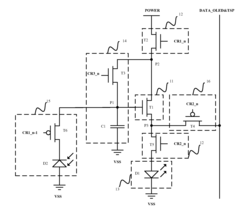
Active matrix organic light emitting diode pixel unit circuit, display panel and electronic product
PatentActiveUS9459721B2
Innovation
- The AMOLED pixel unit circuit is redesigned to include a light emitting module, a driving module, a threshold compensating module, a light emission controlling module, a touch sensing module, and an induction signal outputting module, which utilize existing data lines and control signals to integrate the TSP in Cell circuit, sharing circuit elements and control signals to minimize additional components.
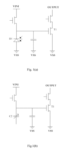
Active Matrix Enhanced Organic Light Emitting Diode Displays for Large Screen Graphic Display Applications
PatentActiveUS20190207126A1
Innovation
- Replacing vacuum-deposited layered structures with a chiral liquid crystalline structure built by solvent casting and photopolymerization, using chiral liquid crystalline band edge emission enhanced OLEDs (C-OLEDs) that form a helical photonic crystal, reducing the number of layers and manufacturing complexity.
Environmental Impact of PC-AMOLED Displays
The integration of photonic crystal structures in AMOLED displays for enhanced durability has significant environmental implications. These advanced displays offer potential benefits in terms of energy efficiency and longevity, which could contribute to reduced electronic waste and lower energy consumption over time.
Photonic crystal-enhanced AMOLED (PC-AMOLED) displays have the potential to improve the overall energy efficiency of devices. By optimizing light extraction and management, these displays can achieve higher brightness levels with lower power consumption. This reduction in energy usage translates to decreased carbon emissions associated with device operation, particularly in regions where electricity generation relies heavily on fossil fuels.
The increased durability of PC-AMOLED displays may lead to extended device lifespans. Longer-lasting displays could reduce the frequency of device replacements, thereby minimizing electronic waste generation. This aligns with circular economy principles and supports sustainable consumption patterns. However, the complex nature of PC-AMOLED displays may present recycling challenges, necessitating the development of specialized recycling processes to recover valuable materials effectively.
Manufacturing PC-AMOLED displays involves sophisticated processes and materials, which may have environmental implications. The production of photonic crystal structures often requires precise nanofabrication techniques, potentially increasing energy consumption and resource utilization during manufacturing. Additionally, the use of rare earth elements or specialized materials in these displays could raise concerns about resource depletion and the environmental impact of mining activities.
Water usage and chemical waste management are critical considerations in the production of PC-AMOLED displays. The fabrication processes may involve water-intensive steps and the use of various chemicals. Proper treatment and disposal of wastewater and chemical byproducts are essential to minimize environmental contamination and protect local ecosystems.
The potential for improved display quality in PC-AMOLED devices could indirectly impact user behavior and device usage patterns. Enhanced visual experiences may lead to increased screen time, potentially resulting in higher energy consumption at the user level. This behavioral aspect should be considered when assessing the overall environmental impact of the technology.
As the technology matures, opportunities for eco-friendly innovations in PC-AMOLED display production may emerge. Research into bio-based materials for photonic crystal structures or the development of more energy-efficient manufacturing processes could further improve the environmental profile of these displays. Continued focus on sustainable design principles and life cycle assessments will be crucial in optimizing the environmental performance of PC-AMOLED technology.
Manufacturing Scalability of PC-AMOLED
The manufacturing scalability of Photonic Crystal (PC) integrated Active-Matrix Organic Light-Emitting Diode (AMOLED) displays presents both significant opportunities and challenges for the industry. As the demand for more durable and efficient display technologies grows, the integration of photonic crystal structures into AMOLED devices has emerged as a promising solution. However, scaling up this technology for mass production requires careful consideration of several factors.
One of the primary challenges in manufacturing PC-AMOLED at scale is the precise fabrication of photonic crystal structures. These nanostructures require highly controlled and uniform patterning processes, which can be difficult to achieve consistently over large areas. Current manufacturing techniques, such as nanoimprint lithography and self-assembly methods, show promise but need further refinement to meet the stringent requirements of high-volume production.
The integration of photonic crystal structures with existing AMOLED manufacturing processes is another critical aspect of scalability. This integration must be seamless and compatible with established production lines to minimize disruption and additional costs. Developing processes that can incorporate PC structures without compromising the performance or yield of AMOLED devices is essential for successful scaling.
Material selection and optimization play a crucial role in the scalability of PC-AMOLED manufacturing. The materials used for photonic crystal structures must be compatible with OLED materials and processes while maintaining their optical properties at scale. Research into novel materials and deposition techniques that can meet these requirements is ongoing and will be vital for large-scale production.
Quality control and uniformity across large substrate areas present significant challenges in scaling up PC-AMOLED manufacturing. Ensuring consistent optical properties and durability enhancements across entire displays requires advanced metrology and inspection techniques. Developing robust quality assurance processes that can rapidly assess large numbers of devices is essential for maintaining high yields in mass production.
The cost-effectiveness of PC-AMOLED manufacturing at scale is a critical factor in its commercial viability. While the integration of photonic crystal structures may increase initial production costs, the potential improvements in device longevity and performance could offset these expenses in the long term. Balancing the additional manufacturing complexity with the benefits of enhanced durability will be crucial for widespread adoption of this technology.
Unlock deeper insights with PatSnap Eureka Quick Research — get a full tech report to explore trends and direct your research. Try now!
Generate Your Research Report Instantly with AI Agent
Supercharge your innovation with PatSnap Eureka AI Agent Platform!