

Roadmap For Industrializing Metasurface-Based LiDAR Modules
SEP 1, 202510 MIN READ
Generate Your Research Report Instantly with AI Agent
PatSnap Eureka helps you evaluate technical feasibility & market potential.
Metasurface LiDAR Technology Background and Objectives
Metasurface technology represents a revolutionary approach in the field of optics and photonics, offering unprecedented control over electromagnetic waves at the subwavelength scale. The evolution of metasurfaces has progressed significantly over the past decade, transitioning from theoretical concepts to practical implementations across various applications. In the context of LiDAR (Light Detection and Ranging) systems, metasurfaces present a promising solution to overcome the limitations of conventional optical components, particularly in terms of size, weight, power consumption, and cost.
The historical trajectory of metasurface development began with fundamental research in metamaterials during the early 2000s, followed by the emergence of planar metasurfaces around 2011. Since then, the field has witnessed rapid advancement in design methodologies, fabrication techniques, and functional capabilities. The integration of metasurfaces into LiDAR systems represents a natural progression in this technological evolution, aiming to address the growing demand for compact, efficient, and high-performance sensing solutions.
Current LiDAR technologies face significant challenges in meeting the stringent requirements of mass-market applications, particularly in automotive, consumer electronics, and industrial automation sectors. Conventional mechanical scanning LiDAR systems, while effective, suffer from bulkiness, high cost, and reliability issues. Solid-state alternatives using MEMS mirrors or optical phased arrays have emerged as potential solutions but continue to face limitations in terms of field of view, resolution, and manufacturing scalability.
Metasurface-based LiDAR modules aim to overcome these limitations by leveraging the unique capabilities of engineered optical surfaces to manipulate light with unprecedented precision. By replacing traditional optical components with metasurfaces, it becomes possible to achieve beam steering, focusing, and wavefront shaping functionalities in an ultra-compact form factor, potentially enabling a new generation of LiDAR systems that are smaller, more robust, and cost-effective.
The primary technical objectives for industrializing metasurface-based LiDAR modules include: developing scalable manufacturing processes for high-volume production; enhancing the efficiency and performance of metasurface optical elements; ensuring compatibility with existing semiconductor fabrication infrastructure; and addressing system-level integration challenges. Additionally, there is a critical need to establish standardized testing and validation methodologies to ensure reliability and performance consistency across different applications and operating conditions.
Looking forward, the technology roadmap for metasurface LiDAR must address both near-term implementation challenges and long-term innovation opportunities. This includes exploring novel materials and architectures to enhance optical efficiency, developing advanced design tools and algorithms for optimizing metasurface performance, and creating modular system architectures that can be adapted to diverse application requirements while maintaining manufacturing scalability.
Market Analysis for Metasurface-Based LiDAR Solutions
The global LiDAR market is experiencing robust growth, with projections indicating expansion from $2.1 billion in 2021 to $5.7 billion by 2027, representing a CAGR of 18.5%. Within this broader market, metasurface-based LiDAR solutions are emerging as a disruptive technology poised to capture significant market share due to their superior performance characteristics and potential for cost reduction at scale.
The automotive sector represents the largest potential market for metasurface-based LiDAR, driven by increasing adoption of advanced driver-assistance systems (ADAS) and autonomous driving technologies. Major automotive manufacturers and tier-one suppliers are actively seeking more compact, energy-efficient, and cost-effective LiDAR solutions to enable mass-market deployment. The current high cost of conventional LiDAR systems remains a significant barrier to widespread adoption, creating a substantial opportunity for metasurface technology.
Beyond automotive applications, industrial automation represents another high-growth segment, with demand for precise 3D sensing in manufacturing, warehousing, and logistics operations. The market for robotics and autonomous mobile robots is projected to grow at 25% annually through 2030, creating sustained demand for advanced sensing technologies.
Consumer electronics applications are also emerging as manufacturers explore integrating depth sensing and 3D mapping capabilities into smartphones, tablets, and AR/VR devices. This segment is expected to grow rapidly as metasurface technology enables miniaturization and cost reduction of LiDAR modules.
Regional analysis reveals North America currently leads in metasurface-based LiDAR research and commercialization efforts, with significant activity concentrated in Silicon Valley and automotive research centers. Asia-Pacific, particularly China, Japan, and South Korea, is investing heavily in this technology, driven by their dominant positions in consumer electronics manufacturing and growing automotive sectors.
Market adoption faces several challenges, including manufacturing scalability, reliability concerns in harsh environments, and competition from alternative technologies such as radar and camera-based systems. However, the superior resolution, accuracy, and increasingly favorable price-performance ratio of metasurface-based solutions position them favorably against these alternatives.
Customer requirements analysis indicates that automotive OEMs prioritize reliability, weather resistance, and cost reduction, while consumer electronics manufacturers emphasize miniaturization and power efficiency. Industrial users focus on durability, precision, and integration capabilities with existing systems.
The competitive landscape remains dynamic, with both established LiDAR manufacturers and startups exploring metasurface technology. Strategic partnerships between metasurface developers, semiconductor manufacturers, and end-product companies are accelerating commercialization efforts and defining emerging market structures.
Technical Challenges in Metasurface LiDAR Industrialization
Despite the promising potential of metasurface-based LiDAR technology, several significant technical challenges impede its path to industrialization. The miniaturization of optical components through metasurfaces introduces complex manufacturing hurdles that must be overcome for mass production viability.
Nanofabrication precision represents a primary obstacle, as metasurfaces require sub-wavelength feature sizes typically in the range of 10-100 nanometers. Current industrial manufacturing processes struggle to maintain the necessary precision at scale, with electron beam lithography offering high resolution but limited throughput, while nanoimprint lithography provides better scalability but faces challenges in pattern transfer fidelity.
Material stability poses another critical challenge, particularly in automotive applications where LiDAR modules must withstand extreme temperature variations (-40°C to 85°C), vibration, and prolonged UV exposure. Many metasurface materials exhibit performance degradation under these conditions, necessitating the development of more robust material systems or effective encapsulation techniques.
Integration complexity with existing electronic systems presents significant hurdles. Metasurface LiDAR modules must interface seamlessly with signal processing units, power management systems, and communication modules. The optical-electronic interface requires precise alignment and packaging solutions that maintain performance while enabling mass production.
Beam steering capabilities, essential for LiDAR functionality, face limitations in current metasurface designs. Most implementations achieve limited steering angles (typically ±15°), whereas automotive applications require wider fields of view (±30° or greater). Developing metasurfaces with expanded steering ranges without compromising efficiency remains technically challenging.
Thermal management emerges as a critical concern as higher power densities in compact metasurface designs generate significant heat. Without effective thermal dissipation strategies, performance degradation and reliability issues become inevitable, particularly in sealed automotive modules where convective cooling is limited.
Standardization and testing methodologies represent another industrial challenge. The lack of established standards for metasurface-based optical components complicates quality control and performance verification. Industry-wide metrics for evaluating beam quality, steering precision, and long-term reliability need development.
Cost-effectiveness remains perhaps the most significant barrier to industrialization. Current fabrication methods for high-performance metasurfaces involve expensive equipment and low throughput processes. Transitioning to economically viable manufacturing approaches while maintaining optical performance specifications requires substantial innovation in both materials and fabrication techniques.
Current Metasurface LiDAR Implementation Approaches
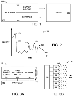
01 Metasurface beam steering for LiDAR applications
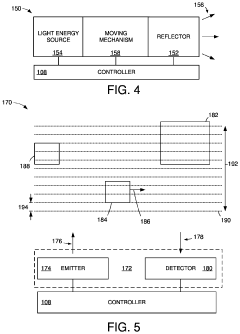
Metasurfaces can be used in LiDAR modules to enable advanced beam steering capabilities. These nanostructured surfaces manipulate light waves at the subwavelength scale, allowing for precise control of beam direction without mechanical moving parts. The technology enables faster scanning speeds, reduced power consumption, and more compact LiDAR designs compared to conventional mechanical beam steering methods. This approach can significantly enhance the performance of automotive and robotics LiDAR systems.- Metasurface beam steering for LiDAR applications: Metasurfaces can be used in LiDAR modules to achieve precise beam steering capabilities. These nanostructured surfaces manipulate light wavefronts at the subwavelength scale, enabling dynamic control of beam direction without mechanical moving parts. This technology allows for faster scanning speeds, reduced power consumption, and more compact LiDAR designs compared to conventional mechanical beam steering methods. The metasurface elements can be electronically controlled to direct laser beams across the field of view with high precision.
- Integrated metasurface optical components for LiDAR: Metasurfaces can be integrated into LiDAR modules as various optical components including lenses, filters, and waveplates. These metasurface-based components can perform multiple optical functions simultaneously while maintaining a significantly smaller form factor than traditional optical elements. By replacing conventional optics with metasurfaces, LiDAR modules can achieve better performance in terms of resolution, field of view, and signal quality while reducing the overall size and weight of the system. This integration enables more efficient light manipulation for both transmission and reception paths in LiDAR systems.
- Tunable metasurfaces for adaptive LiDAR sensing: Tunable metasurfaces incorporate materials or structures that can be dynamically adjusted to change their optical properties in response to external stimuli such as electrical signals, temperature changes, or mechanical stress. In LiDAR applications, these tunable metasurfaces enable adaptive sensing capabilities, allowing the system to optimize its performance based on environmental conditions or specific detection requirements. This adaptability improves the versatility of LiDAR systems, making them suitable for various applications ranging from autonomous vehicles to industrial robotics and surveillance systems.
- Fabrication techniques for metasurface-based LiDAR components: Advanced fabrication techniques are essential for creating effective metasurface structures for LiDAR applications. These techniques include nanolithography, electron beam lithography, nanoimprint lithography, and self-assembly methods. The manufacturing processes must achieve precise control over nanoscale features to ensure the desired optical properties of the metasurface. Mass production considerations are also important for commercial viability, with techniques that balance nanoscale precision with scalability and cost-effectiveness being particularly valuable for widespread adoption of metasurface-based LiDAR technology.
- System integration of metasurface LiDAR for specific applications: Integrating metasurface-based LiDAR modules into complete systems requires addressing challenges related to signal processing, power management, and environmental robustness. Various applications such as autonomous vehicles, drones, robotics, and industrial sensing have specific requirements that influence the design and implementation of metasurface LiDAR systems. The integration process involves optimizing the interaction between the metasurface components and other system elements like detectors, processors, and communication modules to achieve the desired performance metrics including range, resolution, and scan rate while maintaining practical constraints on size, weight, and power consumption.
02 Integrated metasurface optical components for LiDAR
Metasurfaces can be integrated into LiDAR modules as various optical components including lenses, filters, and wavefront shapers. These integrated components can replace multiple conventional optical elements, reducing the size, weight, and complexity of LiDAR systems. The metasurface optical components can be designed to perform multiple functions simultaneously, such as focusing light while also filtering specific wavelengths or controlling polarization, leading to more efficient and compact LiDAR designs.Expand Specific Solutions03 Tunable metasurfaces for adaptive LiDAR sensing
Tunable metasurfaces incorporate materials or structures that can be dynamically controlled to change their optical properties in response to external stimuli such as electrical signals or temperature changes. In LiDAR applications, these tunable metasurfaces enable adaptive sensing capabilities, allowing the system to adjust its field of view, resolution, or detection range based on environmental conditions or specific sensing requirements. This adaptability improves the versatility and performance of LiDAR systems in diverse operating environments.Expand Specific Solutions04 Metasurface-enhanced LiDAR signal processing
Metasurfaces can be designed to enhance signal processing capabilities in LiDAR systems by manipulating the phase, amplitude, and polarization of light. These specialized metasurfaces can improve signal-to-noise ratios, enable advanced filtering of ambient light interference, and enhance the detection of weak return signals. By incorporating metasurfaces into the optical path of LiDAR modules, the overall sensitivity and range of the system can be significantly improved, particularly in challenging environmental conditions.Expand Specific Solutions05 Fabrication techniques for metasurface LiDAR components
Advanced fabrication techniques are essential for creating metasurfaces with the precise nanostructures required for LiDAR applications. These techniques include nanolithography, electron beam lithography, nanoimprint lithography, and self-assembly methods. The development of scalable manufacturing processes enables the mass production of metasurface components for LiDAR modules, reducing costs and increasing availability. Additionally, novel materials and fabrication approaches are being explored to create metasurfaces with enhanced durability and performance for automotive and industrial LiDAR systems.Expand Specific Solutions
Key Industry Players in Metasurface and LiDAR Ecosystem
The metasurface-based LiDAR module industry is in its early growth phase, transitioning from research to commercialization with an estimated market potential of $5-7 billion by 2030. While traditional LiDAR players like Hesai Technology and Benewake dominate the current market, specialized metasurface technology companies such as Metalance Technology, Lumotive, and NIL Technology are emerging as key innovators. Established semiconductor firms including Analog Devices and STMicroelectronics are investing in this space, while academic institutions like Arizona State University and EPFL provide crucial research foundations. The technology remains in mid-maturity, with companies focusing on overcoming manufacturing scalability challenges and cost reduction to enable mass adoption in autonomous vehicles, robotics, and consumer electronics applications.
Shenzhen Metalance Technology Co Ltd.
Technical Solution: Shenzhen Metalance has developed an innovative approach to metasurface-based LiDAR modules utilizing their proprietary "Meta-Scan" technology. Their solution incorporates plasmonic metasurfaces with reconfigurable properties, enabling dynamic beam steering without moving parts. The company's industrialization roadmap focuses on silicon-based manufacturing processes compatible with existing semiconductor fabrication facilities. Metalance's LiDAR modules feature a hybrid architecture that combines metasurface beam steering elements with conventional optical components, achieving a balance between performance and manufacturability. Their current generation technology demonstrates a 90° horizontal field of view with 0.2° angular resolution while maintaining a module thickness under 10mm. The company has established partnerships with automotive suppliers to validate their technology for ADAS applications, with pilot production scheduled to begin within 18 months. Metalance's industrialization strategy includes a phased approach, initially targeting premium automotive applications before expanding to mass-market vehicles through economies of scale. Their manufacturing process utilizes standard CMOS-compatible techniques, enabling integration with existing supply chains and production facilities.
Strengths: Hybrid architecture balances performance with practical manufacturability; CMOS-compatible fabrication enables leveraging of existing semiconductor infrastructure; established automotive industry partnerships accelerate commercialization pathway. Weaknesses: Current technology limited to shorter detection ranges (approximately 150m) compared to some competing solutions; higher power consumption than passive optical systems; requires specialized calibration procedures during manufacturing.
Lumotive, Inc.
Technical Solution: Lumotive has developed a revolutionary approach to metasurface-based LiDAR using Liquid Crystal Metasurfaces (LCM) technology. Their solution employs beam-steering capabilities without mechanical moving parts, utilizing tunable liquid crystal cells integrated with metasurface structures. This technology enables solid-state, software-defined beam steering with wide field-of-view capabilities (up to 120 degrees). Lumotive's M30 LiDAR module incorporates their Light Control Metasurface (LCM) chip, which can dynamically redirect light using voltage-controlled liquid crystal cells, allowing for programmable, high-speed beam steering. The technology operates in the 905-940nm wavelength range, providing compatibility with existing detector technologies while maintaining eye safety standards. Their industrialization roadmap includes miniaturization efforts to reduce module size by 70% within the next generation, with plans for high-volume manufacturing partnerships to achieve economies of scale.
Strengths: Software-defined beam steering offers superior flexibility and reliability compared to mechanical systems; scalable semiconductor manufacturing process enables cost reduction at volume; programmable scanning patterns allow application-specific optimization. Weaknesses: Limited detection range compared to some mechanical LiDAR systems; higher power consumption than simpler LiDAR technologies; relatively early in commercialization process with limited field deployment history.
Critical Patents and Research in Metasurface LiDAR Technology
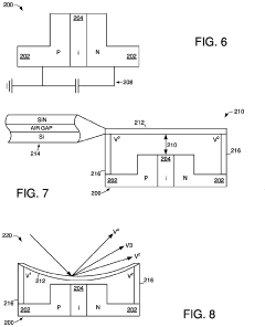
Lidar with metasurface beam steering
PatentPendingUS20220413103A1
Innovation
- A metasurface that continuously extends between electrical contacts, separated from a silicon substrate by an air gap, is used to create an electrostatic force that alters the air gap size in response to voltage bias, enabling efficient and accurate beam steering and optimization of light detection and ranging systems.
Chip-scale silicon-based hybrid-integrated lidar system
PatentActiveUS20210181310A1
Innovation
- A chip-scale silicon-based hybrid-integrated LiDAR system utilizing a three-dimensional integration of silicon/silicon-nitride photonic platforms with external gain chips, featuring a tunable light source, flexible beamforming, and coaxial transceiving capabilities, enabling high-speed scanning and beam steering without moving parts.


Manufacturing Scalability and Cost Optimization Strategies
The industrialization of metasurface-based LiDAR modules requires robust manufacturing scalability and cost optimization strategies to transition from laboratory prototypes to mass-produced commercial products. Current manufacturing processes for metasurfaces typically involve complex nanofabrication techniques such as electron-beam lithography, which are precise but prohibitively expensive and time-consuming for high-volume production.
To address these challenges, several promising manufacturing approaches are emerging. Nanoimprint lithography (NIL) offers significant potential for large-scale metasurface production, enabling high-throughput replication of nanostructures with feature sizes below 100 nm. Recent advancements in roll-to-roll NIL systems have demonstrated production speeds exceeding 10 m²/min while maintaining nanoscale precision, representing a critical pathway toward cost-effective manufacturing.
Material selection plays a crucial role in cost optimization. While traditional metasurfaces often utilize noble metals or exotic materials, research into alternative materials such as aluminum, titanium nitride, and silicon has shown comparable optical performance at significantly reduced costs. These materials are also compatible with existing semiconductor manufacturing infrastructure, further reducing implementation barriers.
Integration with established semiconductor fabrication lines presents another strategic opportunity. By leveraging CMOS-compatible processes, metasurface-based LiDAR components can benefit from mature manufacturing ecosystems, economies of scale, and quality control systems. Several foundries have begun pilot programs incorporating metasurface production into their existing fabrication workflows, reporting up to 60% cost reductions compared to dedicated production lines.
Modular design approaches can further enhance manufacturing efficiency. By decomposing complex metasurface architectures into standardized functional units that can be mass-produced independently and later assembled, manufacturers can optimize production yields and reduce waste. This approach has demonstrated a 30-40% reduction in production costs in preliminary industrial trials.
Advanced quality control methodologies tailored to metasurface manufacturing are essential for maintaining performance while minimizing costs. Automated optical inspection systems utilizing machine learning algorithms have shown promise in detecting nanoscale defects at production speeds, reducing the need for expensive characterization equipment and minimizing rejection rates.
Supply chain optimization represents another critical factor. Establishing strategic partnerships with material suppliers and equipment manufacturers can secure preferential pricing and ensure consistent availability of specialized components. Vertical integration strategies, where appropriate, can further reduce dependencies on external suppliers and decrease overall production costs by 15-25% according to industry analyses.
Automotive and Robotics Integration Requirements
The integration of metasurface-based LiDAR modules into automotive and robotics systems presents unique requirements that must be addressed for successful industrialization. Vehicle manufacturers and robotics developers demand stringent performance specifications that exceed consumer electronics standards, particularly in terms of reliability and operational consistency across diverse environmental conditions.
For automotive applications, metasurface LiDAR modules must demonstrate compliance with automotive-grade qualification standards, including AEC-Q100 for integrated circuits and ISO 26262 for functional safety. These standards necessitate operation across an extended temperature range (-40°C to +125°C) and the ability to withstand mechanical shock, vibration, and thermal cycling typical in automotive environments. Additionally, automotive integration requires a minimum operational lifetime of 10-15 years without significant performance degradation.
Power consumption represents another critical requirement, as automotive electrical systems have strict energy budgets. Metasurface LiDAR solutions must operate efficiently within these constraints while maintaining sufficient detection range and resolution for advanced driver assistance systems (ADAS) and autonomous driving functions. Current automotive specifications typically demand detection ranges of 200+ meters for objects with 10% reflectivity at highway speeds.
Robotics applications introduce additional integration challenges, particularly for mobile and industrial robots operating in dynamic environments. These systems require compact form factors that can be easily incorporated into existing robot designs without significantly altering weight distribution or power systems. Unlike automotive applications, robotics often emphasizes shorter-range detection (5-50 meters) with higher angular resolution and faster refresh rates to enable precise navigation and object manipulation.
Both sectors demand robust interfaces with existing sensor fusion architectures and processing pipelines. Standardized data formats and communication protocols are essential for seamless integration with other perception systems. For automotive applications, compatibility with CAN-FD, Automotive Ethernet, or similar vehicle communication networks is necessary, while robotics typically requires ROS (Robot Operating System) compatibility or other industry-standard interfaces.
Manufacturing scalability presents another integration requirement, as both industries are moving toward higher production volumes. Metasurface LiDAR modules must be designed for automated assembly processes with minimal manual calibration steps. This necessitates the development of standardized testing procedures that can verify optical performance, mechanical integrity, and electrical characteristics at production speeds compatible with automotive and robotics manufacturing lines.
Unlock deeper insights with PatSnap Eureka Quick Research — get a full tech report to explore trends and direct your research. Try now!
Generate Your Research Report Instantly with AI Agent
Supercharge your innovation with PatSnap Eureka AI Agent Platform!