

Metrology Techniques For Characterizing Subwavelength Beam Control
SEP 1, 202510 MIN READ
Generate Your Research Report Instantly with AI Agent
PatSnap Eureka helps you evaluate technical feasibility & market potential.
Subwavelength Beam Control Metrology Background and Objectives
Subwavelength beam control represents a critical frontier in optical engineering, enabling manipulation of light at scales smaller than its wavelength. The evolution of this technology traces back to the early 2000s when researchers began exploring near-field optics and plasmonics to overcome the diffraction limit. Over the past two decades, significant advancements in nanofabrication techniques, computational electromagnetics, and material science have accelerated progress in this domain.
The technological trajectory has moved from theoretical concepts to practical implementations across various applications including high-resolution imaging, nanolithography, optical data storage, and quantum information processing. Recent breakthroughs in metamaterials and metasurfaces have further expanded the possibilities for subwavelength beam manipulation, enabling unprecedented control over light's amplitude, phase, and polarization at nanoscale dimensions.
Current trends indicate a convergence of subwavelength beam control with other emerging technologies such as artificial intelligence, integrated photonics, and quantum optics. This integration promises to unlock new capabilities in fields ranging from biomedical imaging to telecommunications and computing. The miniaturization of optical components continues to drive innovation, with researchers pursuing ever-smaller feature sizes and greater functionality.
The primary technical objective of metrology techniques for characterizing subwavelength beam control is to develop precise, reliable, and non-destructive methods to measure and validate optical performance at scales below the diffraction limit. This includes quantifying beam properties such as focal spot size, intensity distribution, wavefront characteristics, and polarization states with nanometer-scale resolution.
Additional objectives include establishing standardized measurement protocols that enable consistent evaluation across different laboratories and applications, developing real-time monitoring capabilities for dynamic subwavelength phenomena, and creating metrology solutions compatible with manufacturing environments to support quality control in production settings.
The ultimate goal is to bridge the gap between theoretical models and experimental implementations by providing accurate feedback mechanisms that can inform iterative design improvements. As subwavelength beam control technologies advance toward commercial applications, robust metrology becomes increasingly essential for validating performance claims, ensuring reproducibility, and accelerating technology transfer from research laboratories to industrial settings.
Furthermore, these metrology techniques must evolve to address emerging challenges such as characterizing three-dimensional beam profiles, measuring transient phenomena at ultrafast timescales, and quantifying quantum properties of subwavelength optical fields. The development of such advanced measurement capabilities will be crucial for unlocking the full potential of subwavelength beam control across scientific and industrial applications.
Market Applications and Demand Analysis for Nanoscale Beam Characterization
The market for nanoscale beam characterization technologies is experiencing robust growth, driven primarily by the semiconductor industry's relentless pursuit of smaller feature sizes and more complex architectures. As chip manufacturers continue to push beyond the 3nm node toward 2nm and below, the demand for advanced metrology techniques capable of characterizing subwavelength beam control has become increasingly critical. Current market estimates value the semiconductor metrology and inspection equipment sector at approximately $7.5 billion, with a compound annual growth rate of 6.8% projected through 2028.
Beyond semiconductors, emerging applications in nanophotonics, quantum computing, and advanced materials science are creating new market segments for subwavelength beam characterization tools. The nanophotonics market, valued at $39.2 billion, requires precise beam control for developing next-generation optical computing components, integrated photonic circuits, and meta-optical devices. These applications demand metrology solutions capable of measuring phase, polarization, and intensity distributions at nanometer scales.
The biomedical sector represents another significant growth area, particularly in super-resolution microscopy and nanoscale imaging. Research institutions and pharmaceutical companies are investing heavily in technologies that enable visualization of subcellular structures and biomolecular interactions, creating a specialized market segment estimated at $1.2 billion for advanced optical characterization tools.
Defense and aerospace industries are also driving demand for subwavelength beam characterization, particularly for applications in directed energy systems, advanced sensing, and secure communications. These sectors value metrology techniques that can verify the performance of beam-steering components and wavefront shaping devices operating at the diffraction limit.
Regional analysis reveals that Asia-Pacific, particularly Taiwan, South Korea, and China, dominates market demand due to concentrated semiconductor manufacturing. North America leads in research applications, while Europe shows strong growth in photonics and quantum technology applications.
Customer requirements are evolving toward non-destructive, in-line measurement capabilities with higher throughput and reduced measurement uncertainty. End-users increasingly demand metrology solutions that can characterize complex beam parameters including orbital angular momentum, vectorial properties, and spatiotemporal characteristics at nanometer resolution.
Market barriers include the high cost of equipment acquisition and operation, with advanced metrology systems often exceeding $1 million, limiting adoption to large corporations and well-funded research institutions. Additionally, the technical complexity of these systems requires specialized expertise, creating opportunities for service-based business models alongside equipment sales.
Current Metrology Challenges in Subwavelength Regime
The characterization of subwavelength beam control presents significant metrology challenges that continue to push the boundaries of measurement science. As optical and photonic technologies advance toward manipulating light at scales smaller than its wavelength, conventional measurement techniques encounter fundamental limitations. The diffraction limit, approximately half the wavelength of light, has traditionally constrained optical microscopy and measurement systems, making it difficult to accurately characterize structures and phenomena at the subwavelength scale.
Current metrology systems face several critical challenges when applied to subwavelength beam control. First, there is the resolution barrier - conventional far-field optical techniques cannot directly resolve features smaller than approximately 200-300 nm for visible light. This limitation becomes particularly problematic when characterizing metasurfaces, photonic crystals, and other nanophotonic devices that operate by manipulating light at scales of tens to hundreds of nanometers.
Signal-to-noise ratio presents another significant challenge. As measurement targets decrease in size, the scattered or emitted signal becomes increasingly weak relative to background noise. This necessitates sophisticated signal processing and noise reduction techniques, which themselves can introduce artifacts or measurement uncertainties that are difficult to quantify.
Phase measurement represents a particularly complex challenge in subwavelength metrology. Many subwavelength beam control devices operate by manipulating the phase of light, yet phase information is not directly accessible through intensity measurements. Current interferometric techniques struggle to provide accurate phase mapping at subwavelength scales, especially for complex wavefronts with rapid spatial variations.
The dynamic nature of many beam control systems further complicates measurement efforts. Techniques capable of capturing time-resolved data at subwavelength spatial resolution remain limited, constraining our ability to characterize transient phenomena and dynamic beam manipulation processes. This temporal-spatial measurement gap represents a significant bottleneck in advancing active and tunable subwavelength optical technologies.
Calibration and standardization pose additional challenges. The lack of universally accepted measurement standards for subwavelength optical characterization leads to inconsistencies between different measurement approaches and laboratories. This hampers reproducibility and slows the development of reliable design rules for subwavelength optical components.
Finally, there exists a fundamental disconnect between near-field and far-field measurement techniques. Near-field scanning optical microscopy (NSOM) can achieve subwavelength resolution but measures evanescent fields that may not directly correlate with the propagating far-field that ultimately determines device performance in many applications. Bridging this measurement gap remains an ongoing challenge for comprehensive characterization of subwavelength beam control systems.
State-of-the-Art Subwavelength Beam Characterization Methods
01 Optical metrology techniques
Optical metrology techniques utilize light-based measurements for precise characterization of surfaces, structures, and materials. These methods include interferometry, scatterometry, and spectroscopic analysis that can detect nanometer-scale features. Optical techniques offer advantages of being non-destructive, providing high resolution, and enabling real-time monitoring of manufacturing processes. These approaches are particularly valuable in semiconductor fabrication and quality control applications.- Optical metrology techniques: Optical metrology techniques utilize light-based measurements to characterize surfaces, dimensions, and properties of materials. These techniques include interferometry, scatterometry, and spectroscopic methods that provide non-destructive, high-precision measurements. They are particularly valuable in semiconductor manufacturing and quality control processes where nanometer-scale precision is required. These methods can measure critical dimensions, film thickness, and surface topography with exceptional accuracy.
- In-situ process monitoring and control: In-situ metrology techniques enable real-time monitoring and control of manufacturing processes. These systems integrate measurement capabilities directly into production equipment, allowing for immediate feedback and process adjustments. This approach reduces production delays, improves yield, and ensures consistent quality by detecting and correcting deviations as they occur. Applications include chemical mechanical polishing, semiconductor fabrication, and advanced manufacturing where process parameters must be tightly controlled.
- Advanced surface characterization methods: Advanced surface characterization methods provide detailed information about surface properties, including roughness, defects, and composition. These techniques employ various physical principles such as electron microscopy, atomic force microscopy, and profilometry to generate high-resolution data about surface features. They are essential for quality control in precision manufacturing, materials science research, and development of advanced materials where surface properties significantly impact performance.
- Computational metrology and modeling: Computational metrology combines measurement data with sophisticated algorithms and models to extract more information than direct measurements alone can provide. These techniques include machine learning approaches, simulation-based analysis, and digital twins that enhance measurement interpretation and prediction capabilities. By integrating physical measurements with computational methods, these approaches improve accuracy, enable virtual metrology, and support predictive maintenance in manufacturing environments.
- Multi-sensor integration and data fusion: Multi-sensor integration combines data from multiple metrology instruments to provide more comprehensive characterization than any single technique can offer. These systems integrate different measurement principles such as optical, mechanical, and electrical methods to characterize complex features and properties. Data fusion algorithms combine these diverse inputs to generate unified, high-confidence measurements that overcome the limitations of individual sensors and provide more complete characterization of complex materials and structures.
02 In-situ process monitoring and control
In-situ metrology techniques enable real-time monitoring and control of manufacturing processes. These systems integrate measurement capabilities directly into production equipment, allowing for immediate feedback and adjustment. By continuously monitoring critical parameters during fabrication, these techniques help maintain process stability, reduce defects, and improve yield. Applications include chemical mechanical polishing, semiconductor manufacturing, and advanced materials processing.Expand Specific Solutions03 Machine learning and AI-enhanced metrology
Advanced metrology systems increasingly incorporate machine learning and artificial intelligence to enhance measurement capabilities. These intelligent systems can identify patterns in complex measurement data, predict process deviations, and automatically classify defects. By leveraging computational algorithms, these techniques improve measurement accuracy, reduce false positives, and enable more sophisticated analysis of manufacturing processes. This approach is particularly valuable for handling large datasets and complex geometries in modern manufacturing environments.Expand Specific Solutions04 Semiconductor and microelectronics metrology
Specialized metrology techniques have been developed for the semiconductor and microelectronics industries to characterize increasingly complex and miniaturized structures. These methods focus on critical dimensions, overlay accuracy, film thickness, and defect detection at nanometer scales. Advanced techniques include electron microscopy, atomic force microscopy, and specialized optical methods adapted for semiconductor materials. These approaches support the development and manufacturing of high-performance integrated circuits and microelectronic devices.Expand Specific Solutions05 Multi-sensor and hybrid metrology systems
Multi-sensor and hybrid metrology systems combine multiple measurement technologies to provide comprehensive characterization of complex samples. By integrating different measurement principles such as optical, mechanical, and electrical techniques, these systems overcome the limitations of individual methods. This approach enables more complete material and process characterization, improves measurement confidence through cross-validation, and extends the range of measurable parameters. Applications include advanced manufacturing, materials science, and quality control in various industries.Expand Specific Solutions
Leading Research Groups and Industrial Players in Nanometrology
The metrology techniques for subwavelength beam control market is currently in a growth phase, with increasing demand driven by semiconductor manufacturing advancements. The market size is expanding as miniaturization trends continue across electronics industries. Technologically, this field is reaching maturity in established applications while evolving for emerging needs. Leading players include ASML Netherlands BV, which dominates lithography systems, and KLA Corp., specializing in process control and metrology solutions. Samsung Electronics, Huawei, and QUALCOMM are investing heavily in this technology for next-generation devices. Companies like Nova Ltd. and NTT are advancing specialized metrology techniques, while research institutions such as MIT and Electronics & Telecommunications Research Institute are pioneering novel approaches for subwavelength characterization.
ASML Netherlands BV
Technical Solution: ASML has developed advanced metrology techniques for subwavelength beam control in their lithography systems. Their approach combines optical and electron beam technologies with computational metrology. Their YieldStar optical metrology system uses scatterometry and advanced algorithms to measure critical dimensions and overlay accuracy at nanometer scales. For subwavelength structures, ASML employs coherent diffraction imaging and phase retrieval algorithms to reconstruct high-resolution images of features below the diffraction limit. Their holistic lithography concept integrates metrology directly into the manufacturing process, using real-time feedback loops to adjust exposure parameters based on measured deviations. ASML's computational metrology leverages machine learning algorithms to enhance measurement accuracy and speed, enabling the characterization of increasingly complex 3D structures at sub-wavelength dimensions.
Strengths: Industry-leading integration of metrology with lithography systems enables closed-loop process control; proprietary algorithms provide exceptional measurement accuracy at extreme scales. Weaknesses: High system complexity requires significant expertise to operate; solutions are primarily optimized for semiconductor manufacturing rather than broader applications.
KLA Corp.
Technical Solution: KLA has pioneered comprehensive metrology solutions specifically designed for subwavelength beam control characterization. Their portfolio includes the SpectraFilm and SpectraShape systems that utilize multi-angle spectroscopic ellipsometry and scatterometry to measure critical dimensions and profiles of subwavelength structures with nanometer precision. KLA's approach combines optical techniques with advanced modeling algorithms that simulate light-structure interactions to extract dimensional information beyond conventional resolution limits. Their Archer overlay metrology systems employ diffraction-based measurements with sophisticated image processing to achieve sub-nanometer precision in alignment verification. KLA has also developed hybrid metrology frameworks that combine multiple measurement techniques (optical, e-beam, and AFM) with statistical analysis to improve overall accuracy and reliability. Their latest systems incorporate machine learning algorithms that continuously improve measurement models based on correlations with reference measurements.
Strengths: Unmatched precision in dimensional metrology with demonstrated sub-nanometer repeatability; comprehensive suite of complementary techniques provides complete characterization capabilities. Weaknesses: Systems typically require significant capital investment; complex calibration procedures necessary to maintain accuracy across different material stacks and feature geometries.
Critical Patents and Literature in Subwavelength Metrology
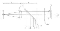
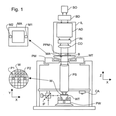
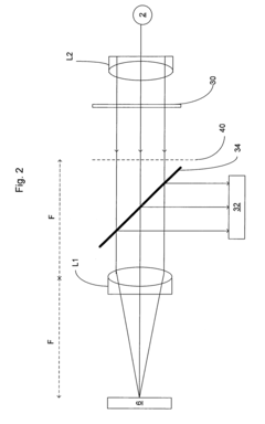
Metrology apparatus, lithographic apparatus, process apparatus, metrology method and device manufacturing method
PatentInactiveUS20070002336A1
Innovation
- A metrology apparatus utilizing a supercontinuum light source to generate a measurement beam, combined with an optical system to direct the beam onto a substrate and a sensor to detect reflected or diffracted radiation, enhancing sensitivity and speed.
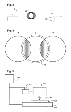
Metrology method with beams incident on a target at a plurality of different angles of incidence and associated metrology tool
PatentInactiveEP4414785A1
Innovation
- A metrology tool and method utilizing a dispersive element to scatter source radiation, focusing the scattered radiation onto a target at different angles of incidence, and detecting the second scattered radiation to enhance signal diversity and resolution, employing a focusing mirror element with a hollow prolate spheroid portion and high harmonic generation for EUV and SXR radiation.
Standardization Efforts in Nanometrology
The standardization of nanometrology techniques for subwavelength beam control has become increasingly critical as nanofabrication and characterization technologies advance. Several international organizations are actively working to establish unified measurement protocols and reference standards that ensure consistency and reliability across different laboratories and industries.
The International Organization for Standardization (ISO) has established Technical Committee 229 specifically focused on nanotechnologies, which has published several standards relevant to subwavelength metrology. These include ISO/TS 80004 series defining terminology and ISO/TS 21363 addressing measurements of particle size and shape distributions. For subwavelength beam characterization specifically, ISO/TC 172/SC 9 has developed standards for optical measurement methods that are being adapted for nanoscale applications.
The National Institute of Standards and Technology (NIST) in the United States has pioneered reference materials and calibration techniques for nanometrology. Their Advanced Nanoscale Metrology Program has developed Standard Reference Materials (SRMs) for calibrating instruments used in subwavelength beam characterization, including specialized photomask linewidth standards and atomic force microscopy calibration grids with features below 100 nm.
In Europe, the European Metrology Programme for Innovation and Research (EMPIR) has funded several projects focused on standardizing nanometrology techniques. The "3DNano" and "NanoMag" projects specifically address three-dimensional nanoscale measurements and magnetic nanostructure characterization, both relevant to subwavelength beam control applications.
The International Bureau of Weights and Measures (BIPM) has established the Consultative Committee for Length (CCL) working group on nanometrology, which coordinates international comparisons of nanoscale measurement capabilities. Their recent work includes standardizing measurement protocols for near-field optical techniques used in subwavelength beam characterization.
Industry consortia are also contributing significantly to standardization efforts. The Semiconductor Equipment and Materials International (SEMI) organization has developed standards for metrology in semiconductor manufacturing that address subwavelength features, including SEMI MS5 for photomask specifications and SEMI MS8 for phase-shifting mask metrology.
Challenges in standardization include the rapid evolution of measurement technologies, the complexity of nanoscale phenomena, and the diversity of application requirements. Current efforts are focusing on establishing traceability chains from macro to nanoscale, developing consensus on measurement uncertainty calculations, and creating accessible reference materials that can be widely distributed to calibrate instruments across different laboratories and manufacturing facilities.
Integration with Advanced Manufacturing Processes
The integration of metrology techniques for subwavelength beam control with advanced manufacturing processes represents a critical frontier in precision engineering. Current manufacturing technologies increasingly demand real-time measurement capabilities that can be seamlessly incorporated into production workflows. In-line metrology systems capable of characterizing subwavelength features during fabrication processes enable immediate feedback loops, significantly reducing production errors and enhancing yield rates in nanophotonic device manufacturing.
Advanced manufacturing platforms such as molecular beam epitaxy (MBE) and atomic layer deposition (ALD) systems are now being equipped with integrated optical metrology tools that can monitor beam characteristics at subwavelength scales without disrupting the deposition process. These hybrid systems utilize specialized optical paths and detection schemes that operate in parallel with the primary manufacturing process, providing continuous monitoring without contamination risks or process interruptions.
The semiconductor industry has pioneered several integration approaches, including scatterometry-based process control systems that can be directly incorporated into lithography equipment. These systems utilize specialized algorithms to extract subwavelength beam characteristics from scattered light patterns, enabling real-time adjustments to exposure parameters. Similar principles are being adapted for other manufacturing contexts where beam control is critical, such as in directed energy deposition and laser-based additive manufacturing.
Challenges in this integration domain primarily revolve around maintaining measurement accuracy under actual production conditions. Vibration, thermal fluctuations, and process-induced contaminants can all degrade metrology performance. Advanced isolation systems and environmental controls are being developed specifically to address these challenges, including active vibration cancellation technologies and thermally stabilized optical paths that maintain calibration during extended manufacturing runs.
Data handling represents another significant consideration in integrated metrology systems. The volume of measurement data generated during continuous monitoring of subwavelength beam characteristics necessitates sophisticated data processing architectures. Edge computing solutions are increasingly being deployed to process metrology data at the point of collection, extracting actionable insights without overwhelming central manufacturing execution systems.
Industry 4.0 frameworks are accelerating this integration by providing standardized protocols for metrology data exchange between manufacturing subsystems. These protocols enable metrology-driven feedback to propagate across multiple process steps, creating holistic control systems that can maintain beam characteristics throughout complex manufacturing sequences. The resulting closed-loop manufacturing systems represent a significant advancement in precision control for nanophotonic and quantum optical device production.
Unlock deeper insights with PatSnap Eureka Quick Research — get a full tech report to explore trends and direct your research. Try now!
Generate Your Research Report Instantly with AI Agent
Supercharge your innovation with PatSnap Eureka AI Agent Platform!