Integration Of Metasurfaces With VCSEL Arrays For Compact LiDAR
SEP 1, 20259 MIN READ
Generate Your Research Report Instantly with AI Agent
Patsnap Eureka helps you evaluate technical feasibility & market potential.
Metasurface-VCSEL LiDAR Integration Background & Objectives
LiDAR (Light Detection and Ranging) technology has evolved significantly over the past decades, transforming from bulky, expensive systems primarily used in specialized applications to increasingly compact solutions targeting mass-market deployment. The integration of metasurfaces with Vertical-Cavity Surface-Emitting Laser (VCSEL) arrays represents a cutting-edge technological convergence that promises to revolutionize LiDAR systems for autonomous vehicles, robotics, and consumer electronics.
The historical trajectory of LiDAR development began with mechanical scanning systems in the 1960s, progressing through solid-state approaches in the early 2000s. Recent years have witnessed an accelerated push toward miniaturization and cost reduction, driven by automotive and consumer electronics demands. VCSELs emerged as promising light sources due to their compact size, low power consumption, and mass-production compatibility, while metasurfaces—engineered surfaces with subwavelength structures—have demonstrated unprecedented capabilities in manipulating light properties.
The fundamental technical objective of integrating metasurfaces with VCSEL arrays is to overcome the inherent limitations of conventional LiDAR systems, particularly size constraints, power efficiency, and manufacturing scalability. This integration aims to enable beam steering and shaping functionalities without mechanical components, potentially reducing system size by orders of magnitude while maintaining or improving performance metrics.
Current technological trends indicate growing interest in all-solid-state LiDAR solutions, with particular emphasis on semiconductor-based approaches. The metasurface-VCSEL integration represents a logical progression in this evolution, leveraging advances in nanofabrication, semiconductor manufacturing, and optical design to create highly integrated photonic systems.
The primary technical goals for this integration include achieving wide-angle beam steering (>120°), high resolution (<0.1°), fast scanning rates (>kHz), and maintaining high optical efficiency (>50%) while reducing form factor to enable integration into consumer devices. Additionally, the technology aims to support multi-beam operation for parallel scanning and 3D imaging capabilities.
From a manufacturing perspective, the objective extends to developing processes compatible with semiconductor fabrication techniques, enabling high-volume production at competitive cost points. This includes addressing challenges in metasurface design for broadband operation, polarization independence, and temperature stability—all critical for automotive-grade reliability.
The convergence of these technologies aligns with broader industry trends toward edge computing and distributed sensing networks, where compact, energy-efficient LiDAR modules could serve as key enablers for next-generation intelligent systems across multiple industries.
Market Analysis for Compact LiDAR Solutions
The LiDAR market is experiencing significant growth, with the global market valued at approximately $1.8 billion in 2021 and projected to reach $5.7 billion by 2027, representing a CAGR of 21.6%. This growth is primarily driven by increasing adoption in autonomous vehicles, robotics, industrial automation, and smart infrastructure applications. The automotive sector remains the largest consumer of LiDAR technology, accounting for over 60% of market demand.
Compact LiDAR solutions are emerging as a particularly high-growth segment within this market. Traditional mechanical LiDAR systems, while effective, are bulky, expensive, and have moving parts that reduce reliability. This has created substantial market demand for more compact, cost-effective alternatives that maintain or improve performance metrics.
The integration of metasurfaces with VCSEL arrays represents a promising approach to addressing these market needs. This technology combination offers significant size reduction potential, with estimates suggesting up to 80% volume reduction compared to conventional systems. Cost projections indicate potential manufacturing cost reductions of 30-50% at scale, making LiDAR more accessible for mass-market applications.
Consumer electronics companies are showing increasing interest in compact LiDAR solutions for smartphone depth sensing, augmented reality applications, and gesture recognition. This represents a new market segment with high volume potential but demanding cost constraints, typically requiring solutions under $10 per unit.
Regional analysis shows North America leading the LiDAR market with approximately 40% share, followed by Europe and Asia-Pacific. However, Asia-Pacific, particularly China, is experiencing the fastest growth rate due to rapid adoption in manufacturing automation and smart city initiatives.
Customer requirements for compact LiDAR solutions vary by application but commonly include range capabilities of 100-200 meters for automotive applications, 10-50 meters for robotics, and 0.1-5 meters for consumer electronics. Resolution requirements similarly vary from 0.1° for automotive to 1-2° for consumer applications.
Market barriers include price sensitivity, with automotive OEMs targeting sub-$500 LiDAR units for mass adoption. Technical performance requirements remain stringent despite cost pressures, with customers expecting improvements in range, resolution, and power efficiency alongside size reduction.
The competitive landscape is evolving rapidly, with established LiDAR manufacturers like Velodyne and Ouster facing competition from startups focused on solid-state and compact solutions. Technology companies with expertise in optics and semiconductor manufacturing are increasingly entering this space, recognizing the potential of integrated photonic approaches like metasurface-VCSEL combinations.
Current Challenges in Metasurface-VCSEL Integration
The integration of metasurfaces with VCSEL arrays presents several significant technical challenges that currently impede widespread commercial adoption for compact LiDAR systems. Fabrication compatibility remains a primary obstacle, as metasurfaces typically require nanoscale precision manufacturing processes that differ substantially from established VCSEL production methods. The disparate material systems and processing requirements create integration difficulties when attempting to combine these technologies on a single substrate or in a compact package.
Thermal management presents another critical challenge. VCSELs generate considerable heat during operation, which can alter the optical properties of metasurfaces through thermal expansion and refractive index changes. This thermal crosstalk can significantly degrade beam steering accuracy and overall system performance, particularly in high-power applications required for longer-range LiDAR sensing.
Bandwidth limitations also constrain current integration efforts. While metasurfaces excel at manipulating specific wavelengths, creating broadband metasurfaces that maintain consistent performance across the operational spectrum of VCSELs remains technically challenging. This wavelength dependency limits the flexibility of integrated systems and can impact sensing accuracy across variable environmental conditions.
Beam quality preservation during steering represents another substantial hurdle. Current metasurface designs often introduce wavefront aberrations when steering VCSEL beams at large angles, resulting in beam distortion and reduced optical efficiency. These effects directly impact the range and resolution capabilities of LiDAR systems, particularly at the extreme angles required for wide field-of-view applications.
Scalability concerns further complicate integration efforts. Manufacturing metasurface-VCSEL combinations at the scale required for automotive or consumer electronics applications demands high-volume production capabilities that maintain nanoscale precision while achieving acceptable yield rates. Current fabrication approaches struggle to meet these dual requirements cost-effectively.
Power efficiency also remains suboptimal in current integration schemes. Metasurfaces typically introduce additional optical losses that reduce the overall system efficiency, a critical factor for battery-powered applications like autonomous vehicles or mobile devices. These losses compound the already challenging power budget constraints of compact LiDAR systems.
Finally, packaging and reliability issues persist across different integration approaches. Environmental factors such as temperature fluctuations, humidity, and mechanical vibration can affect the long-term stability of metasurface-VCSEL systems. Developing robust packaging solutions that protect these sensitive optical components while maintaining precise alignment and compact form factors represents a significant engineering challenge that has yet to be fully resolved.
Existing Metasurface-VCSEL Integration Approaches
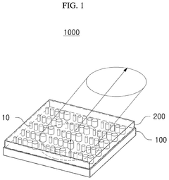
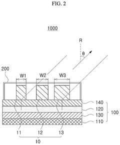
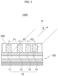
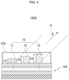
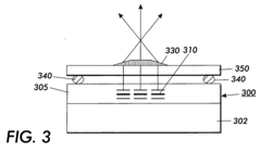
01 Integration of metasurfaces with VCSEL arrays for beam shaping
Metasurfaces can be integrated with VCSEL arrays to enable advanced beam shaping capabilities. These integrated systems allow for precise control of the beam profile, divergence, and direction. The metasurface structures, typically consisting of subwavelength optical elements, can transform the output beam from VCSELs into desired patterns while maintaining a compact form factor. This approach eliminates the need for bulky external optics and enables sophisticated beam manipulation directly at the source.- Integration of metasurfaces with VCSEL arrays for beam shaping: Metasurfaces can be integrated with VCSEL arrays to enable advanced beam shaping capabilities. These integrated systems allow for precise control of the beam profile, divergence, and direction. The metasurface structures, typically consisting of subwavelength elements, can transform the output beam from VCSELs into desired patterns or profiles, enhancing the functionality of the overall system while maintaining a compact form factor.
- Compact metasurface-VCSEL integration techniques: Various techniques have been developed to achieve compact integration of metasurfaces with VCSEL arrays. These include monolithic integration where the metasurface is directly fabricated on the VCSEL surface, hybrid integration approaches using bonding techniques, and wafer-level integration methods. These techniques focus on minimizing the overall device footprint while maintaining optical performance, thermal management, and manufacturing feasibility.
- Polarization control in metasurface-integrated VCSEL arrays: Metasurfaces integrated with VCSEL arrays can provide enhanced polarization control capabilities. The metasurface structures can be designed to manipulate the polarization state of the emitted light, enabling functionalities such as polarization conversion, generation of vector beams, or polarization-dependent beam steering. This capability is particularly valuable for applications requiring specific polarization states while maintaining the compact form factor of the integrated device.
- Wavelength-selective metasurfaces for VCSEL array applications: Wavelength-selective metasurfaces can be integrated with VCSEL arrays to enable spectral filtering, wavelength division multiplexing, or wavelength-dependent beam manipulation. These structures can be designed to respond differently to various wavelengths, allowing for compact multi-wavelength operation or wavelength-specific beam control. This approach enables more complex functionality within a single compact device, reducing the need for additional optical components.
- Fabrication methods for compact metasurface-VCSEL integration: Advanced fabrication methods have been developed to achieve compact integration of metasurfaces with VCSEL arrays. These include nanoimprint lithography, electron beam lithography, and other nanofabrication techniques that enable the creation of precise subwavelength structures directly on or near VCSEL emitters. These methods focus on maintaining alignment accuracy, ensuring compatibility with existing VCSEL fabrication processes, and achieving high-volume manufacturing capability while preserving the compact nature of the devices.
02 Compact polarization control in VCSEL-metasurface systems
Metasurfaces integrated with VCSEL arrays can provide compact and efficient polarization control functionality. By designing specific metasurface patterns, the polarization state of the emitted light can be manipulated, allowing for circular, linear, or complex polarization outputs. This integration eliminates the need for separate polarization control components, significantly reducing the overall system size while enhancing functionality. The metasurface elements can be designed to operate at the VCSEL emission wavelength for optimal performance.Expand Specific Solutions03 Wavelength-selective metasurfaces for VCSEL array applications
Wavelength-selective metasurfaces can be integrated with VCSEL arrays to create compact multi-wavelength systems. These metasurfaces can filter, split, or combine different wavelengths emitted from the VCSEL array, enabling wavelength division multiplexing in a minimal footprint. The metasurface structures can be designed to have specific spectral responses that match the VCSEL emission characteristics. This integration is particularly valuable for sensing, communications, and spectroscopic applications where multiple wavelengths must be precisely controlled within a compact device.Expand Specific Solutions04 Fabrication techniques for integrated VCSEL-metasurface devices
Advanced fabrication techniques enable the integration of metasurfaces with VCSEL arrays while maintaining compactness. These methods include monolithic integration where the metasurface is directly fabricated on the VCSEL structure, and hybrid integration where separately fabricated metasurfaces are bonded to VCSEL arrays. Nanoimprint lithography, electron beam lithography, and other nanofabrication techniques allow for precise patterning of metasurface elements at the required subwavelength scale. These fabrication approaches ensure alignment accuracy and mechanical stability while preserving the compact form factor of the integrated device.Expand Specific Solutions05 Thermal management in compact VCSEL-metasurface systems
Effective thermal management is crucial for compact VCSEL-metasurface integrated systems. The close proximity of components in these compact designs can lead to thermal challenges that affect performance and reliability. Advanced thermal management approaches include the use of heat-dissipating materials, optimized device geometries, and thermal isolation structures. Some designs incorporate thermally conductive substrates or micro-channels for heat extraction. Proper thermal management ensures stable operation of the VCSEL array while maintaining the optical performance of the metasurface structures, even in highly compact configurations.Expand Specific Solutions
Key Industry Players in Metasurface and VCSEL Technologies
The integration of metasurfaces with VCSEL arrays for compact LiDAR is currently in an early growth phase, with market size projected to expand significantly as autonomous vehicles and advanced sensing applications gain traction. The technology maturity varies across players, with companies like Lumentum, Trumpf Photonic Components, and ams-Osram leading in VCSEL manufacturing expertise, while Hesai Technology and SOS LAB are advancing integrated LiDAR solutions. Research institutions including the Institute of Semiconductors CAS and Huazhong University are driving fundamental innovations in metasurface integration. The competitive landscape features established optoelectronics manufacturers competing with specialized startups like Vertilite and Vixar, with automotive and consumer electronics companies like Huawei and Samsung increasingly investing in this space to secure strategic positioning in next-generation sensing technologies.
Lumentum Operations LLC
Technical Solution: Lumentum has developed advanced integration solutions combining VCSEL arrays with metasurfaces for LiDAR applications. Their technology utilizes wafer-level integration of metasurface optical elements directly onto VCSEL arrays, creating a monolithic structure that significantly reduces the form factor of traditional LiDAR systems. The metasurfaces are designed with subwavelength nanostructures that manipulate light phase, amplitude, and polarization, enabling beam steering capabilities without mechanical components. Lumentum's approach incorporates multi-layer metasurfaces that can simultaneously perform beam collimation, splitting, and steering functions, eliminating the need for multiple discrete optical components. Their VCSEL arrays feature high-power density (>2W/mm²) and can be arranged in 1D or 2D configurations with individual addressability for dynamic beam forming. The integration process maintains thermal management capabilities critical for high-power VCSEL operation while achieving optical efficiencies exceeding 85% for the metasurface elements.
Strengths: Industry-leading wafer-level integration capabilities, high optical efficiency, and significant size reduction compared to conventional systems. Their technology eliminates moving parts, increasing reliability while reducing power consumption. Weaknesses: The complex fabrication process may impact manufacturing yields and costs. The technology may face challenges in extreme environmental conditions where thermal expansion could affect the metasurface performance.
Hesai Technology Co. Ltd.
Technical Solution: Hesai has developed an innovative approach to integrating metasurfaces with VCSEL arrays for their next-generation automotive LiDAR systems. Their technology utilizes a modular design where custom-designed metasurface optical elements are integrated with high-power VCSEL array modules to create compact, solid-state beam steering capabilities. Hesai's VCSEL arrays feature proprietary designs with enhanced thermal management that enables sustained high-power operation without degradation. The metasurface elements employ silicon nitride nanostructures fabricated using deep UV lithography processes, achieving precise phase control across the optical aperture. Their integration approach maintains critical alignment between the VCSEL emitters and corresponding metasurface elements while allowing for mass production using automated assembly techniques. Hesai's technology enables programmable beam patterns with steering capabilities of ±25° in both horizontal and vertical directions. The integrated modules achieve significant size reduction compared to their mechanical scanning counterparts while maintaining detection ranges exceeding 200 meters with centimeter-level resolution, suitable for advanced driver assistance systems and autonomous driving applications.
Strengths: Proven expertise in automotive LiDAR systems, robust design for harsh environmental conditions, and scalable manufacturing capabilities. Weaknesses: The current technology may have limitations in achieving extremely wide field-of-view without mechanical assistance, and the complex integration process requires specialized equipment that impacts production costs.
Critical Patents in Metasurface-Enhanced LiDAR
Lidar device comprising a plurality of beam steering cells for steering a laser beam
PatentPendingUS20250020783A1
Innovation
- A LiDAR device utilizing a metasurface with nanopillars to steer a laser beam, forming subwavelength patterns that enable efficient beam steering and scanning, allowing for a compact, solid-state design capable of three-dimensional scanning with VCSEL elements arranged in arrays for both vertical and horizontal directions.
Integration of vcsel array and microlens for optical scanning
PatentInactiveEP1317038A3
Innovation
- Integration of a refractive microlens onto a VCSEL array using flip-chip bonding, allowing for directional control of optical output from individual pixels without moving parts, enabling scanning across various wavelengths and materials, and adaptable to one-dimensional, two-dimensional, or circular arrays.
Manufacturing Scalability Assessment
The manufacturing scalability of integrating metasurfaces with VCSEL arrays represents a critical factor in determining the commercial viability of compact LiDAR systems. Current manufacturing processes primarily rely on semiconductor fabrication techniques, including photolithography, electron-beam lithography, and nanoimprint lithography. These established methods offer varying degrees of precision, throughput, and cost-effectiveness.
Photolithography provides high throughput but faces resolution limitations when fabricating sub-wavelength metasurface features. Electron-beam lithography delivers exceptional resolution but suffers from low throughput and high equipment costs, making it suitable for prototyping but challenging for mass production. Nanoimprint lithography emerges as a promising middle-ground approach, offering reasonable resolution with improved throughput potential.
The integration of metasurfaces directly onto VCSEL arrays introduces additional manufacturing complexities. Precise alignment between the metasurface elements and the VCSEL emission points is crucial for optimal beam steering performance. Current alignment techniques achieve accuracies of approximately 1-2 μm, whereas next-generation compact LiDAR systems may require sub-micron precision to maximize optical efficiency and beam quality.
Material compatibility presents another significant manufacturing challenge. The thermal expansion coefficient mismatch between metasurface materials and VCSEL semiconductor substrates can lead to delamination or performance degradation during operation. Recent advances in adhesion layers and thermal management strategies have improved reliability, but further optimization remains necessary for automotive-grade durability requirements.
Cost analysis indicates that current manufacturing approaches result in per-unit costs approximately 5-8 times higher than conventional LiDAR systems. However, economies of scale and manufacturing learning curves suggest potential for 60-70% cost reduction within 3-5 years as production volumes increase. The transition from silicon-based to polymer-based metasurfaces could further reduce manufacturing costs by enabling roll-to-roll processing techniques.
Quality control and yield management represent additional manufacturing considerations. Metasurface defects can significantly impact beam quality and steering precision. Current manufacturing processes achieve approximately 70-80% yield rates, with defect densities around 0.5-1 defects/cm². Improving these metrics requires advanced in-line inspection technologies and refined process controls to detect and mitigate nanoscale fabrication errors before final integration with VCSEL arrays.
Automotive Safety Standards Compliance
The integration of metasurfaces with VCSEL arrays for compact LiDAR systems must comply with stringent automotive safety standards to ensure reliable operation in diverse driving conditions. These systems are subject to regulations such as ISO 26262, which establishes a framework for functional safety in automotive electronics. Compliance with this standard requires comprehensive hazard analysis and risk assessment throughout the development lifecycle of LiDAR systems.
For metasurface-enhanced VCSEL LiDAR to achieve automotive-grade certification, it must demonstrate resilience against environmental stressors defined in standards like AEC-Q100 for integrated circuits. This includes operation across extreme temperature ranges (-40°C to 125°C), resistance to humidity, and tolerance to mechanical shock and vibration. The optical components, particularly the metasurface elements, must maintain precise alignment and performance characteristics under these conditions.
Electromagnetic compatibility (EMC) requirements outlined in CISPR 25 and ISO 11452 present additional compliance challenges. The compact nature of metasurface-VCSEL integration creates potential for electromagnetic interference with other vehicle systems, necessitating careful design considerations and shielding strategies to meet these standards.
Eye safety regulations, particularly IEC 60825 for laser products, impose strict limitations on the maximum permissible exposure levels. This is especially relevant for VCSEL arrays which, when combined with metasurfaces for beam steering, must ensure that focused laser energy remains within Class 1 laser safety parameters under all operating conditions and potential failure modes.
Reliability standards such as AEC-Q102 for optoelectronic components require accelerated life testing to validate the long-term durability of these systems. The novel integration of metasurfaces introduces unique aging mechanisms that must be characterized and mitigated to achieve the 15+ year operational lifespan expected in automotive applications.
Functional performance standards for advanced driver assistance systems (ADAS), including UN Regulation No. 79 for steering equipment and emerging standards for automated driving systems, establish minimum performance criteria for sensing technologies. Metasurface-VCSEL LiDAR systems must demonstrate consistent detection capabilities, range accuracy, and angular resolution across varying environmental conditions to satisfy these requirements.
The certification process for these innovative LiDAR systems requires extensive validation testing, including hardware-in-the-loop simulation and field testing under diverse scenarios. Documentation of safety cases, failure mode analyses, and mitigation strategies must be comprehensive to satisfy regulatory authorities and automotive OEMs' requirements for safety-critical components.
Unlock deeper insights with Patsnap Eureka Quick Research — get a full tech report to explore trends and direct your research. Try now!
Generate Your Research Report Instantly with AI Agent
Supercharge your innovation with Patsnap Eureka AI Agent Platform!