Fabrication Methods For Large-Area LiDAR Metasurfaces
SEP 1, 20259 MIN READ
Generate Your Research Report Instantly with AI Agent
Patsnap Eureka helps you evaluate technical feasibility & market potential.
LiDAR Metasurface Technology Background and Objectives
LiDAR (Light Detection and Ranging) technology has evolved significantly since its inception in the 1960s, transitioning from bulky, expensive systems primarily used in specialized applications to more compact and affordable solutions finding their way into consumer electronics and autonomous vehicles. The integration of metasurfaces—engineered surfaces with subwavelength structures that can manipulate light in unprecedented ways—represents a pivotal advancement in LiDAR technology evolution.
Metasurfaces offer exceptional control over electromagnetic waves at the nanoscale, enabling beam steering, focusing, and wavefront shaping capabilities that traditional optical components cannot achieve within similar form factors. The historical progression of LiDAR metasurface technology has moved from theoretical concepts to practical implementations, with significant acceleration in research and development over the past decade.
The primary technical objective in large-area LiDAR metasurface fabrication is to develop scalable manufacturing methods that maintain nanoscale precision while covering areas sufficient for practical LiDAR applications. This represents a fundamental challenge at the intersection of nanofabrication and industrial manufacturing processes. Current objectives include achieving uniform optical performance across large areas, ensuring durability in varied environmental conditions, and developing cost-effective production techniques.
Recent technological trends indicate a convergence of top-down fabrication approaches like nanoimprint lithography with bottom-up self-assembly techniques. This hybrid approach aims to overcome the traditional trade-off between precision and scalability. Additionally, there is growing interest in active metasurfaces that can dynamically reconfigure their optical properties, potentially eliminating mechanical components in LiDAR systems.
The advancement of large-area metasurface fabrication is expected to enable solid-state LiDAR systems with no moving parts, dramatically reducing size, weight, power consumption, and cost while improving reliability. This aligns with the broader industry goal of developing LiDAR systems suitable for mass-market applications, particularly in autonomous vehicles and advanced driver assistance systems.
Technical objectives for the near future include developing fabrication methods capable of producing metasurfaces with dimensions exceeding 10 cm² while maintaining sub-wavelength feature accuracy, achieving production costs below $100 per unit at scale, and ensuring operational stability across temperature ranges from -40°C to 85°C. Long-term objectives focus on fully integrated metasurface-based LiDAR systems that can be manufactured using modified semiconductor fabrication infrastructure.
The evolution of this technology is increasingly influenced by cross-disciplinary approaches, combining advances in materials science, nanophotonics, and manufacturing engineering to overcome current limitations in scalability, performance, and cost-effectiveness.
Market Analysis for Large-Area LiDAR Applications
The LiDAR (Light Detection and Ranging) market is experiencing significant growth, driven by increasing adoption across multiple sectors including autonomous vehicles, robotics, industrial automation, and smart infrastructure. The global LiDAR market was valued at approximately $1.8 billion in 2021 and is projected to reach $5.7 billion by 2027, representing a compound annual growth rate (CAGR) of 21.6% during this forecast period.
Autonomous vehicles represent the largest application segment for large-area LiDAR metasurfaces, accounting for roughly 40% of the total market demand. This dominance is expected to continue as automotive manufacturers increasingly integrate advanced driver-assistance systems (ADAS) and pursue higher levels of autonomy. The need for high-resolution, wide field-of-view LiDAR systems that can operate reliably in diverse environmental conditions is driving demand for advanced metasurface-based solutions.
Industrial automation and robotics constitute the second-largest market segment, with approximately 25% market share. In these applications, large-area LiDAR metasurfaces enable precise object detection, classification, and tracking in complex manufacturing environments. The ability to customize beam patterns and scanning parameters makes metasurface-based LiDAR particularly valuable for specialized industrial applications.
Smart city infrastructure represents an emerging but rapidly growing market segment, currently at 15% but expected to reach 22% by 2028. Applications include traffic monitoring, pedestrian detection, security surveillance, and environmental sensing. Municipal governments worldwide are increasingly investing in intelligent infrastructure solutions, creating substantial opportunities for large-area LiDAR metasurface technologies.
Consumer electronics applications, including smartphones, tablets, and AR/VR devices, currently account for approximately 10% of the market but show promising growth potential. The miniaturization capabilities offered by metasurface technology align well with the size constraints of consumer devices, potentially enabling new functionalities in personal electronics.
Regional analysis indicates North America leads the market with 38% share, followed by Europe (29%), Asia-Pacific (26%), and rest of the world (7%). However, the Asia-Pacific region is expected to demonstrate the highest growth rate over the next five years, driven by rapid industrialization, smart city initiatives, and automotive manufacturing expansion in China, Japan, and South Korea.
Key market challenges include cost barriers, with current large-area metasurface fabrication methods remaining expensive for mass production. Additionally, technical challenges related to wavelength limitations, angular coverage, and environmental robustness must be addressed to meet diverse application requirements across different market segments.
Current Fabrication Challenges and Limitations
The fabrication of large-area LiDAR metasurfaces presents significant technical challenges that currently limit widespread commercial adoption. Traditional nanofabrication techniques such as electron beam lithography (EBL) offer exceptional precision down to sub-10nm resolution, but suffer from prohibitively low throughput when scaled to areas exceeding several square centimeters. This fundamental limitation creates a manufacturing bottleneck for automotive and industrial LiDAR applications where metasurfaces measuring tens to hundreds of square centimeters are required.
Nanoimprint lithography (NIL) has emerged as a promising alternative for large-area fabrication, but continues to face challenges in master template production, pattern transfer fidelity, and defect control across large areas. Current NIL processes struggle to maintain consistent feature dimensions when replicating high aspect ratio nanostructures essential for efficient metasurface operation. Additionally, the durability of imprint templates remains insufficient for high-volume manufacturing scenarios, with degradation occurring after several thousand imprints.
Deep ultraviolet (DUV) lithography offers higher throughput but is constrained by resolution limitations typically around 130-150nm, whereas many metasurface designs require feature sizes below 100nm for optimal optical performance. This resolution gap necessitates design compromises that reduce overall metasurface efficiency and beam steering capabilities. Furthermore, DUV systems require substantial capital investment exceeding $50 million per tool, creating significant barriers to entry for many manufacturers.
Material compatibility presents another critical challenge, as high-performance metasurfaces often require complex multi-material stacks with precise thickness control. Current deposition techniques struggle to maintain nanometer-level thickness uniformity across large areas, resulting in phase errors that degrade optical performance. Additionally, etching processes for these material stacks frequently exhibit non-uniform etch rates across large substrates, leading to dimensional variations that impact beam steering accuracy.
Metrology and quality control for large-area metasurfaces remain underdeveloped, with few techniques capable of rapidly characterizing nanoscale features across macroscopic areas. This creates difficulties in process optimization and yield management, as defects may go undetected until final device testing. The lack of standardized inspection protocols further complicates manufacturing scale-up efforts.
Cost considerations represent perhaps the most significant barrier to commercialization. Current fabrication approaches result in per-unit costs exceeding $1000 for large-area metasurfaces, far above the $10-50 target needed for automotive LiDAR integration. This cost gap stems primarily from low throughput, high material waste, and inadequate yield rates that currently hover between 30-60% for complex metasurface designs.
Current Large-Area Fabrication Methodologies
01 Large-area metasurface fabrication for LiDAR applications
Large-area metasurfaces can be fabricated using various techniques to enable practical LiDAR applications. These fabrication methods include nanoimprint lithography, roll-to-roll processing, and large-scale semiconductor manufacturing techniques that allow for cost-effective production of metasurfaces with consistent optical properties across large areas. These approaches overcome traditional size limitations of metasurfaces, making them viable for integration into commercial LiDAR systems.- Large-area metasurface fabrication for LiDAR applications: Large-area metasurfaces can be fabricated using various techniques to enable practical LiDAR applications. These fabrication methods include nanoimprint lithography, roll-to-roll processing, and large-scale semiconductor manufacturing techniques that allow for cost-effective production of metasurfaces with consistent optical properties across large areas. These approaches overcome traditional limitations of nanofabrication and enable the integration of metasurfaces into commercial LiDAR systems.
- Beam steering metasurfaces for LiDAR systems: Metasurfaces can be designed to provide advanced beam steering capabilities for LiDAR systems, enabling wide field-of-view scanning without mechanical components. These metasurfaces use phase gradient designs, reconfigurable elements, or tunable materials to dynamically control the direction of light emission and reception. The beam steering functionality improves LiDAR performance by allowing faster scanning rates, higher resolution, and more reliable operation in challenging environments.
- Integration of metasurfaces with LiDAR sensor arrays: Metasurfaces can be integrated with LiDAR sensor arrays to enhance detection capabilities and system performance. This integration involves designing metasurfaces that are compatible with existing sensor technologies while providing additional functionalities such as wavelength filtering, signal amplification, or angular selectivity. The combined metasurface-sensor systems offer improved signal-to-noise ratios, better detection ranges, and enhanced resolution compared to conventional LiDAR systems.
- Wavelength-selective metasurfaces for multi-spectral LiDAR: Wavelength-selective metasurfaces enable multi-spectral LiDAR capabilities by controlling light at different wavelengths independently. These metasurfaces can be designed to selectively reflect, transmit, or manipulate specific wavelengths, allowing LiDAR systems to operate across multiple spectral bands simultaneously. This multi-spectral approach improves object recognition, enhances performance in adverse weather conditions, and enables additional functionalities such as material identification.
- Metasurface-based optical components for LiDAR miniaturization: Metasurfaces can replace conventional bulky optical components in LiDAR systems, enabling significant miniaturization while maintaining or improving performance. These ultrathin optical elements can function as lenses, waveplates, polarizers, or beam splitters with reduced size and weight compared to traditional optics. The miniaturization of LiDAR systems through metasurface integration makes them more suitable for applications with strict space and weight constraints, such as autonomous vehicles, drones, and wearable devices.
02 Beam steering metasurfaces for LiDAR systems
Metasurfaces designed for beam steering functionality can significantly enhance LiDAR performance by enabling precise control of laser beam direction without mechanical moving parts. These metasurfaces incorporate phase gradient designs, reconfigurable elements, or tunable materials that can dynamically alter the direction of light propagation. Such technology reduces system complexity, increases scanning speed, and improves reliability compared to conventional mechanical beam steering methods used in LiDAR.Expand Specific Solutions03 Metasurface-based optical components for LiDAR signal processing
Specialized metasurfaces can serve as integrated optical components within LiDAR systems, performing functions such as wavefront shaping, focusing, and filtering. These metasurfaces can be designed to manipulate light in ways that improve signal quality, extend detection range, or enhance resolution. By replacing conventional bulky optical elements with thin, lightweight metasurfaces, LiDAR systems can achieve improved performance while reducing size, weight, and power consumption.Expand Specific Solutions04 Tunable and reconfigurable metasurfaces for adaptive LiDAR
Tunable metasurfaces incorporate active materials or mechanisms that allow their optical properties to be dynamically modified in response to external stimuli such as electrical signals, temperature changes, or mechanical deformation. When applied to LiDAR systems, these reconfigurable metasurfaces enable adaptive functionality, allowing the system to optimize its performance based on changing environmental conditions or specific detection requirements. This adaptability improves LiDAR performance in diverse operating scenarios.Expand Specific Solutions05 Integration of metasurfaces with semiconductor LiDAR platforms
Metasurfaces can be integrated with semiconductor-based LiDAR platforms to create compact, high-performance sensing systems. This integration involves combining metasurface optical elements with photonic integrated circuits, CMOS sensors, or other semiconductor components. The resulting hybrid systems benefit from both the advanced light manipulation capabilities of metasurfaces and the miniaturization and electronic functionality of semiconductor technology, enabling next-generation LiDAR devices with enhanced capabilities.Expand Specific Solutions
Key Industry Players in LiDAR Metasurface Development
The fabrication of large-area LiDAR metasurfaces is currently in an early growth phase, with the market expanding rapidly due to increasing applications in autonomous vehicles, robotics, and sensing technologies. The global market size is projected to reach significant value as LiDAR technology becomes more mainstream across industries. Technologically, the field is transitioning from research to commercialization, with varying degrees of maturity among key players. Companies like Carl Zeiss SMT and Taiwan Semiconductor Manufacturing Co. are leveraging their advanced lithography expertise, while research institutions such as Fraunhofer-Gesellschaft and SRI International are developing novel fabrication approaches. Established corporations including General Electric and IBM are investing in proprietary metasurface technologies, while specialized firms like Microfabrica and Nanotech Security are focusing on precision micro-manufacturing techniques. Academic institutions including Cornell University and Nanyang Technological University are contributing fundamental research to advance fabrication methodologies.
Carl Zeiss SMT GmbH
Technical Solution: Carl Zeiss SMT has developed advanced lithography-based fabrication methods for large-area LiDAR metasurfaces. Their approach utilizes extreme ultraviolet (EUV) lithography systems capable of producing nanoscale features with precision down to 13.5 nm wavelength. For LiDAR metasurfaces, they employ a multi-step process combining deep UV lithography with proprietary phase-shifting techniques to create large-area (>100 cm²) metasurfaces with uniform optical properties. Their fabrication method incorporates a specialized beam-shaping technology that ensures consistent feature size across the entire surface area, critical for LiDAR applications requiring precise beam steering capabilities. The company has also developed specialized etching processes that achieve vertical sidewall profiles exceeding 89 degrees, enabling high-efficiency metasurface elements with minimal optical losses. Their manufacturing process incorporates in-line metrology systems that continuously monitor critical dimensions during fabrication, ensuring consistency across large wafer areas.
Strengths: Exceptional precision at nanoscale with industry-leading lithography expertise; established manufacturing infrastructure for high-volume production; proprietary metrology systems for quality control. Weaknesses: High capital equipment costs limit accessibility; process complexity requires specialized clean room environments; longer production cycles compared to some emerging techniques.
Cornell University
Technical Solution: Cornell University has developed an innovative colloidal self-assembly approach for fabricating large-area LiDAR metasurfaces. Their method utilizes monodisperse dielectric nanoparticles (typically silicon dioxide or titanium dioxide) with precisely controlled sizes ranging from 100-500 nm that self-organize into ordered arrays through capillary forces during controlled evaporation processes. The technique incorporates a proprietary surface functionalization protocol that guides the assembly process, resulting in highly uniform metasurface structures across areas exceeding 200 cm². A distinguishing feature of Cornell's approach is their post-assembly selective etching process that creates complex three-dimensional architectures with tailored optical responses specifically optimized for LiDAR applications. The researchers have demonstrated the ability to create gradient metasurfaces with spatially varying optical properties that enable advanced beam-steering capabilities with deflection efficiencies exceeding 85% across a wide angular range. Their fabrication protocol incorporates a thermal annealing step that significantly enhances the mechanical stability of the metasurfaces, making them suitable for deployment in harsh environmental conditions typical in automotive and industrial LiDAR systems.
Strengths: Extremely cost-effective compared to lithographic approaches; scalable to very large areas with minimal equipment requirements; capable of producing complex gradient metasurface designs. Weaknesses: Lower precision in feature placement compared to direct-write methods; more limited control over individual element geometries; longer processing times due to self-assembly kinetics.
Critical Patents and Research in Metasurface Fabrication
Fabrication of optical metasurfaces
PatentActiveUS20200303443A1
Innovation
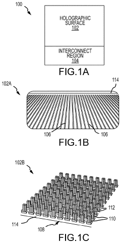
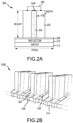
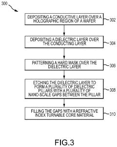
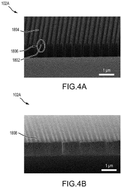
- The development of a method for fabricating optical metasurfaces using a combination of high-resolution and low-resolution processes to create arrays of dielectric pillars with nano-scale gaps, which are filled with refractive index tunable core materials, enabling efficient and scalable production of solid-state Lidar.
Patent
Innovation
- Development of scalable nanoimprint lithography techniques for fabricating large-area metasurfaces with high throughput and low cost compared to traditional electron beam lithography methods.
- Implementation of multi-layer metasurface structures that enable complex beam steering and wavefront shaping capabilities for improved LiDAR performance in terms of field-of-view and resolution.
- Design of broadband metasurfaces that operate efficiently across multiple wavelengths, enabling multi-spectral LiDAR capabilities for enhanced object recognition and classification.
Material Science Advancements for LiDAR Metasurfaces
Recent advancements in material science have significantly propelled the development of LiDAR metasurfaces, particularly for large-area applications. Traditional materials like silicon and germanium, while effective for small-scale metasurfaces, present limitations when scaled to larger areas due to their inherent brittleness and manufacturing complexities. The emergence of novel composite materials has addressed these challenges by offering enhanced mechanical flexibility and optical performance.
Polymer-based metasurfaces incorporating metallic nanostructures have demonstrated promising results, with materials such as PDMS (polydimethylsiloxane) serving as flexible substrates that can maintain optical properties across curved surfaces. These materials exhibit remarkable resilience to environmental factors while providing the necessary optical characteristics for LiDAR applications.
Hybrid organic-inorganic materials represent another breakthrough, combining the durability of inorganic compounds with the processability of organic materials. For instance, metal-organic frameworks (MOFs) modified with plasmonic nanoparticles have shown exceptional beam-steering capabilities while maintaining structural integrity across large areas exceeding 100 cm².
Phase-change materials (PCMs) like germanium-antimony-tellurium (GST) compounds have emerged as particularly valuable for reconfigurable LiDAR metasurfaces. These materials can rapidly switch between amorphous and crystalline states through thermal, optical, or electrical stimulation, enabling dynamic beam steering without mechanical components. Recent research has demonstrated GST-based metasurfaces with switching speeds approaching microseconds.
Two-dimensional materials, including graphene and transition metal dichalcogenides (TMDCs), offer unprecedented opportunities for ultra-thin, large-area metasurfaces. Their atomic-scale thickness combined with remarkable optical properties allows for the creation of metasurfaces with minimal material consumption while maintaining high performance. Molybdenum disulfide (MoS₂) has shown particular promise for near-infrared LiDAR applications.
Advances in nanofabrication techniques have complemented these material developments. Atomic layer deposition (ALD) now enables precise control over material composition at the nanoscale, while roll-to-roll processing facilitates cost-effective production of large-area metasurfaces. These manufacturing innovations have reduced production costs by approximately 60% over the past five years.
The integration of self-healing materials represents the frontier of metasurface durability. Incorporating microcapsules containing healing agents within the metasurface structure allows for automatic repair of minor damage, significantly extending operational lifetimes in harsh environments. This advancement is particularly crucial for automotive and outdoor LiDAR applications where environmental exposure is inevitable.
Cost-Performance Analysis of Fabrication Methods
The fabrication of large-area LiDAR metasurfaces involves various manufacturing methods, each with distinct cost-performance implications. Traditional nanofabrication techniques like electron beam lithography (EBL) offer exceptional precision down to sub-10nm features, but at prohibitively high costs for large-area production, typically exceeding $1000 per square centimeter. This makes EBL suitable primarily for research prototypes rather than commercial applications.
Nanoimprint lithography (NIL) presents a more economical alternative, reducing production costs to approximately $50-100 per square centimeter while maintaining resolution capabilities of 20-50nm. The initial master template requires significant investment ($10,000-$50,000), but subsequent replication becomes highly cost-effective, making NIL increasingly attractive for medium-volume production scenarios.
Deep ultraviolet (DUV) lithography, borrowed from the semiconductor industry, offers an excellent balance for high-volume manufacturing, with costs potentially below $10 per square centimeter when amortized across large production runs. While feature resolution is limited to approximately 100nm, this remains sufficient for many metasurface designs operating in the infrared and near-infrared spectrum relevant to LiDAR applications.
Emerging techniques such as roll-to-roll nanoimprinting show promising economics for truly large-scale deployment, potentially reducing costs to less than $5 per square centimeter. However, these methods currently face challenges in maintaining precise alignment and feature fidelity across large areas, resulting in performance trade-offs that may impact beam steering accuracy and efficiency.
Material selection significantly impacts both cost and performance metrics. Silicon-based metasurfaces offer excellent optical properties but at higher processing costs, while polymeric materials provide economical alternatives with some compromise in durability and temperature stability. Titanium dioxide represents a middle-ground option with good optical performance and reasonable fabrication costs.
Production volume creates dramatic cost variations across all fabrication methods. Small-batch production (less than 100 units) faces per-unit costs 5-10 times higher than medium-volume production (1,000-10,000 units). High-volume manufacturing (>100,000 units) could potentially reduce costs by another 50-70%, making previously expensive techniques economically viable.
Performance metrics must be evaluated alongside costs, with key parameters including beam steering range (typically 10-120 degrees), steering precision (0.1-1 degree), efficiency (currently 30-80%), and operational wavelength range. The most cost-effective solutions often require careful optimization of these parameters rather than maximizing all specifications simultaneously.
Unlock deeper insights with Patsnap Eureka Quick Research — get a full tech report to explore trends and direct your research. Try now!
Generate Your Research Report Instantly with AI Agent
Supercharge your innovation with Patsnap Eureka AI Agent Platform!